6. Electronics Design
Group assignment:
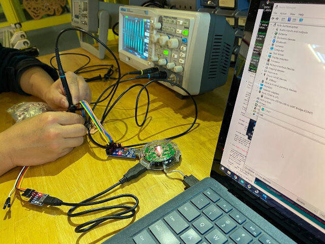
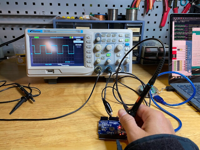
- Use the test equipment in your lab to observe the operation of a microcontroller circuit board (in minimum, check operating voltage on the board with multimeter or voltmeter and use oscilloscope to check noise of operating voltage and interpret a data signal)
Individual assignment:
- Redraw one of the echo hello-world boards
- Add (at least) a button and LED (with current-limiting resistor)
- Check the design rules, make it, test that it can communicate
- Extra credit: simulate its operation.
Learning outcomes
* Select and use software for circuit board design
* Demonstrate workflows used in circuit board design
Designing Electronics with EDA
EDA stands for Electronic Design Automation, it’s a category of software that helps us design circuit boards. The whole process of designing electronics with EDA goes something like this:
- (Decide what you want your electronic device to do and what components you need to make it work… easy!)
- Start with a schematic, a drawing that represents the components in your circuit using symbols and how they’re connected
- Convert schematic into a PCB layout and route physical tracks connecting all the components
- Output PCB design as an SVG or PNG file
- Input SVG/PNG into a CAM software like mods to generate G-code for a CNC mill
- Mill out the PCB (or send to a board house to make for you)
- Stuff the board
- Burn bootloader onto board’s MCU
- Flash program onto board’s MCU
- Test and debug and debug and debug…
- Do stuff with the board that it was designed for!
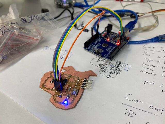
In the case of this week’s assignment, we are to design a new board based off one of Neil’s echo hello-world boards. You say hello to it (through a computer) and it says hello back (the “echo”) in a console. We are to add a tiny bit of complexity to the board with an additional button and LED (at minimum) so that the LED does something when you input a button press.
Setting up KiCad
For EDA software, we have many choices and I chose KiCad because it’s open source and widely used in the industry. It’s also the preferred choice of a respected hardware expert uncle of mine!
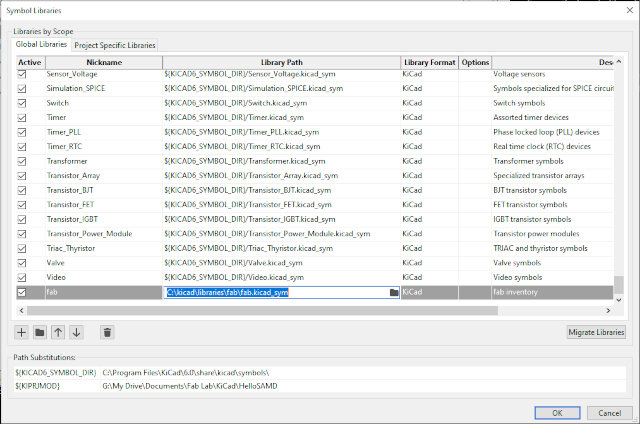
So first I installed KiCad on my computer (Windows 10) and all the Fab Inventory libraries including symbol, footprint, and 3D shapes. Installation instructions can be found in the README file of the Fab Inventory KiCad libraries repo.
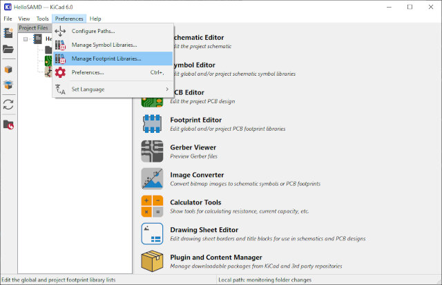
Go to Preferences to manage fab libraries.
Install fab symbols library and confirm.
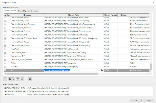
Install fab footprints library and confirm.
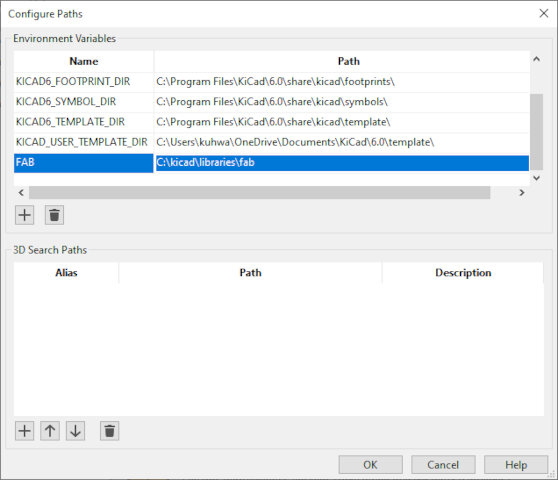
Configure Path to help KiCad find the 3D files of the fab library components.
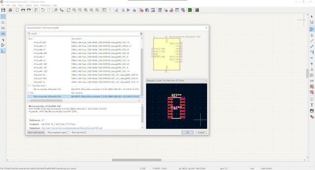
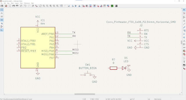
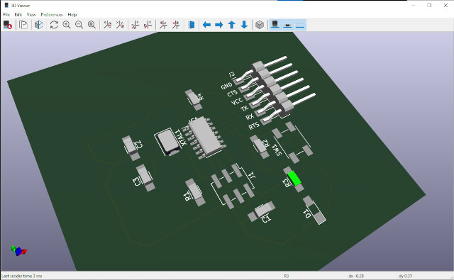
For my board, I chose to start simple with an AVR echo board design using ATtiny44. This is the MCU in the fab library, it’s schematic is on top and the matching PCB footprint is below. There’s even a 3D model of it (no shown).
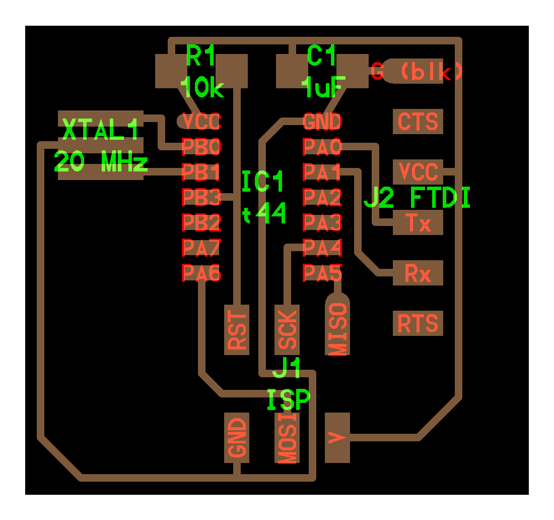
This is the original echo hello-world board for ATtiny44 from Neil.
Looking at the connections in the previously designed PCB I drew my first schematic, and connected all the pins by name directly.
I converted to PCB editor without doing any design check, didn’t know any better! Just wanted to jump in and start messing with the software. Anyways, halfway through I “saved” and closed out to take a break and then coming back KiCad won’t load previously saved files. Did some inspection, noticed save files are cut short for some reason when opening in a text editor.
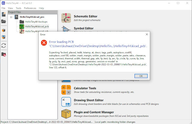
Suspect being in my Google Drive backup folder might be impacting the saving somehow, though never had that problem before. Same story with folders backed up by OneDrive. So,started a new project in a completely local folder and didn’t have any more issues.
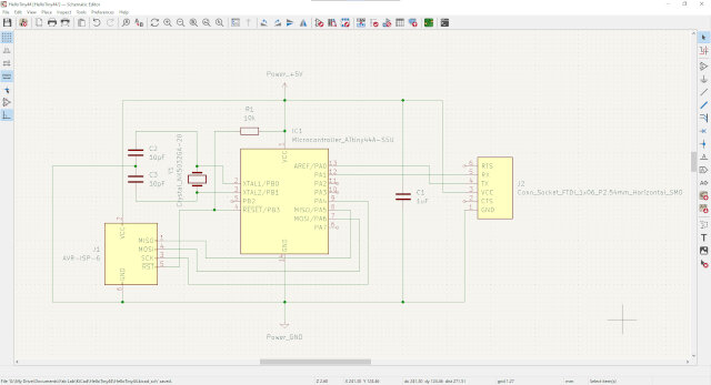
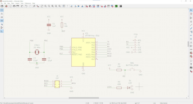
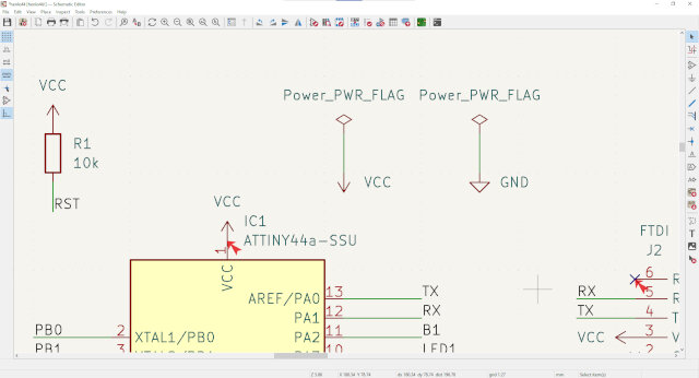
Had to restart my schematic from scratch, but learned some better habits. This time using labels for ease of reading and drawing.
 Schematics are MUCH cleaner using labels instead of actually connecting all the lines. It’s not that important at this point anyways as the real physical routing takes place in the PCB Editor later.
Had some trouble with the J1 ISP connector, needed SMD pads but library object only has through hole. Ended up using generic 2x3 header and referenced other designs for pin assignment in the 2x3 header, connected to VCC, GND, MISO, MOSI, etc. with labels.
Note: button needs a pull-down or pull-up resistor!
Ran the Electrical Rules Checker (ERC) found in top menu bar under the Inspect tab, and got some errors.
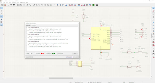
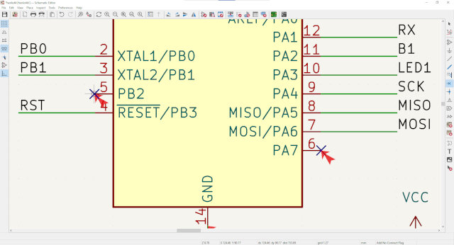
Researching errors, found how to resolve. KiCad doesn’t like pins with no connections, so you have to explicitly tell it if you are not going to connect a pin. On the right-hand side menu bar, select the -x symbol for “Add a no-connection flag”. Add flags to every pin you want to leave unconnected.
Next, you have to explicitly tell ERC where power is coming from with a “PWR_FLAG”
Rerun ERC, no more errors, great success!
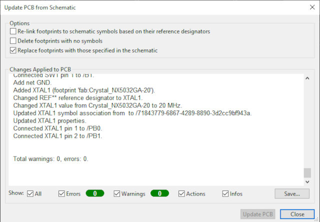
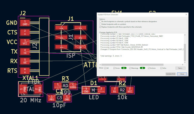
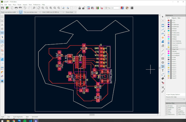
Now onto the hard part, actually making the PCB layout. On top right, click green button for “PCB Editor”. Once PCB Editor is open, on top menu bar click “Update PCB with changes made to schematic” or press F8.
This loads all the footprints into the PCB editor with lines indicating where each of the connections need to go. This is called a “rat’s nest” for some reason. * shrug *
Immediately I noticed something wrong. The footprint for the J1 ISP header connection is wrong. It should be 2x3 surface mount pads like the ones we had in Week 4 when we were making ISP Programmers.
To fix this, I went back to the schematic editor, opened J1’s properties, and in the Footprint field I opened it and found an appropriate one in the fab library.
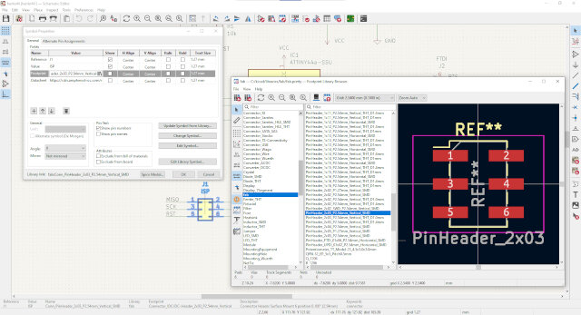
Now we save and then go back to PCB Editor. Again we “Update PCB with changes made to schematic” (F8) and voila! The right footprint we want for the ISP header pads is pulled in.
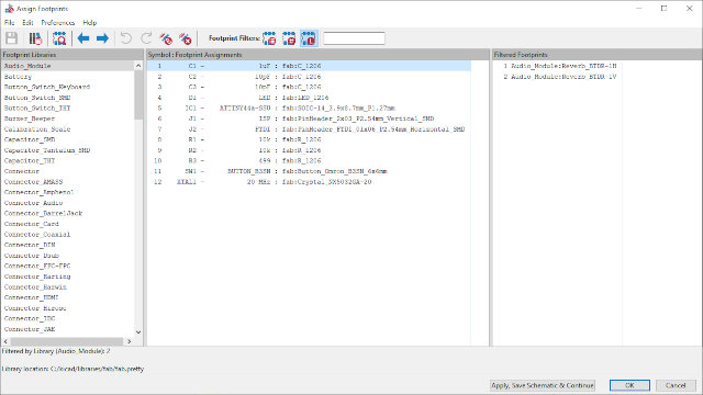
As a double check just to be sure all the footprints are okay, I went back to the Schematic Editor and at the top menu clicked “Run footprint assignment tool”. When selecting Symbols in the first place, I stuck to fab library symbols as much as possible so this shouldn’t be an issue but doesn’t hurt to double check.
Every symbol is assigned to a “fab” footprint so looks like we’re good to go!
Side note: at this point I realized there is an ERC button on the top menu right next to the “Run footprint assignment tool” button lol so that’s even faster than clicking the “Inspect” tab first.
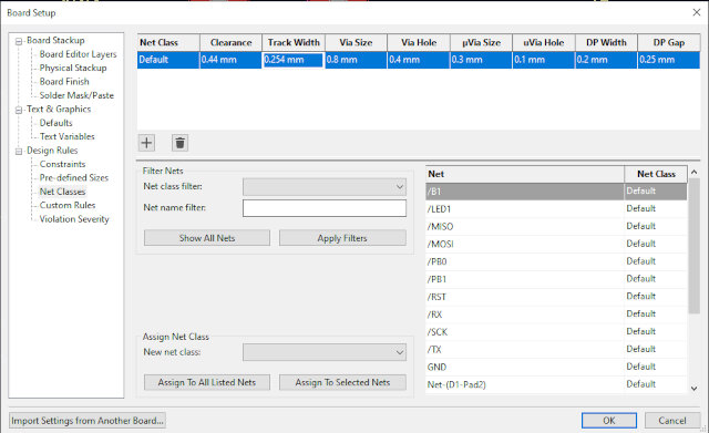
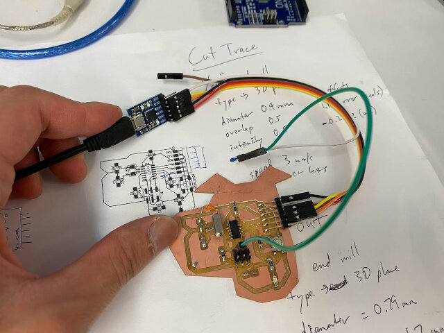
Before starting to make track connections in PCB Editor, we need to set up our board with design rules. Go to File > Board Setup > Net Classes.
From the experiments in Week 4 we know: * min width of trace: 10 mil (thousandth of an inch) = 0.254 mm * min clearance between trace: 17 mil = 0.4318 mm
Set Clearance to 0.44 mm (err on safe side a bit) Set Track Width to 0.254 mm
Then go to Design Rules -> Constraints
Set Minimum track width to 0.254 mm
Hit OK and let’s start connecting pads with the “Route tracks” tool!
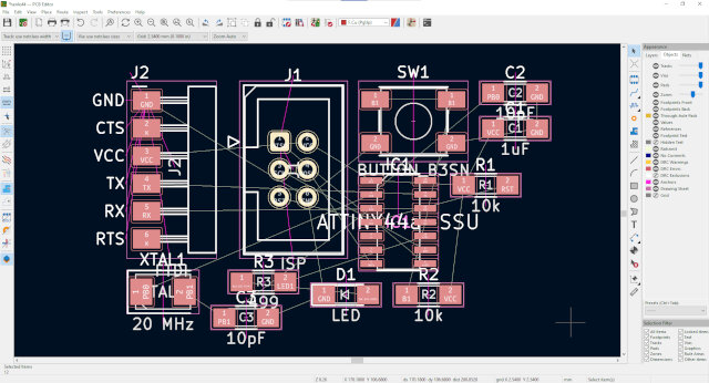
Okay let’s go back to the PCB editor and rat’s nest and start untangling this mess.
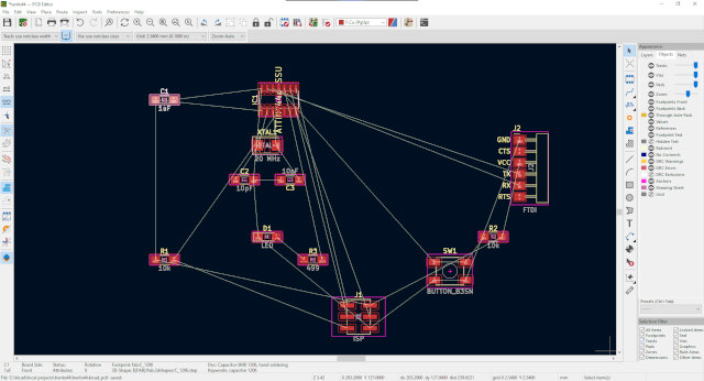
Welp, my first attempt was unsuccessful, a few final pins just were impossible to connect with the spaces left. Was cramming too many pieces above the MCU. There are for sure better strategies to be more efficient at using gaps in between 1206 package footprints and routing VCC and GND around in loops to reach more place more efficiently.
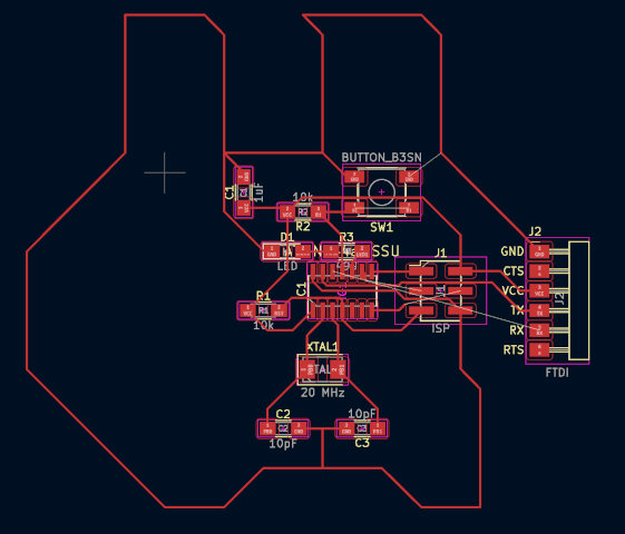
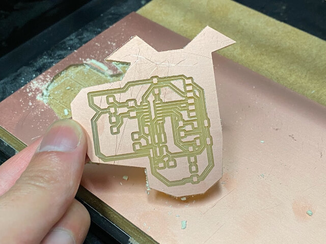
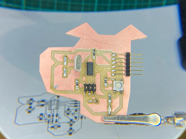
Was trying to be fun last time and making a bunny ears shape, but let’s actually spread out components well and connect everything well first before making fun shapes. I got everything connected except on GND pin to the MCU (kinda important). Couldn’t figure out a better way quickly other than to use a 0 ohm resistor (“R4”) in a 1206 package in order to make a “bridge” to hop over the VCC trace.
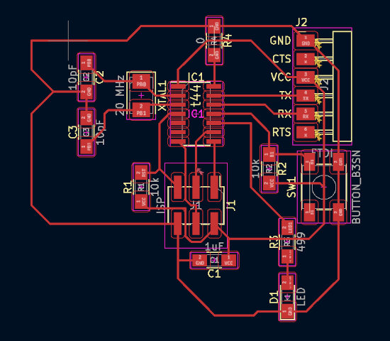
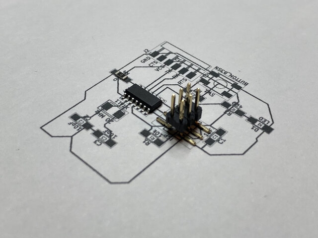
Noticed footprint of 2x3 header looked a little bigger than it was on our Week 4 boards, so did a test print out on paper and matched up a few critical components to make sure everything is fine (and it was). Just need to snip the ends off the 2x3 header to fit on the pads.
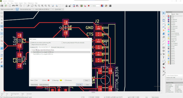
Run Design Rules Checker (DRC), some errors but should be fine to ignore. R4 will be connected with a 0 Ohm resistor so that GND trace will be connected together. The FTDI footprint in the library seems to have some overlap with the silkscreen and the pads, so all the remaining errors are related to that.
Go to Edge.Cuts layer to create a perimeter for the board area.
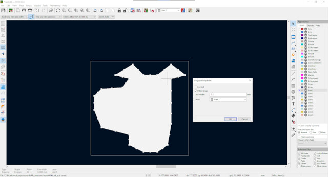
Next change to another layer like User 1, and use “Draw a graphic polygon” tool to draw a shape around your circuits. This is the shape that will actually get cut out. Make sure to change it to a “Filled shape”. Note I had actually jumped ahead to this step earlier, so the doggy outline was changed to different layer after the fact in the properties.
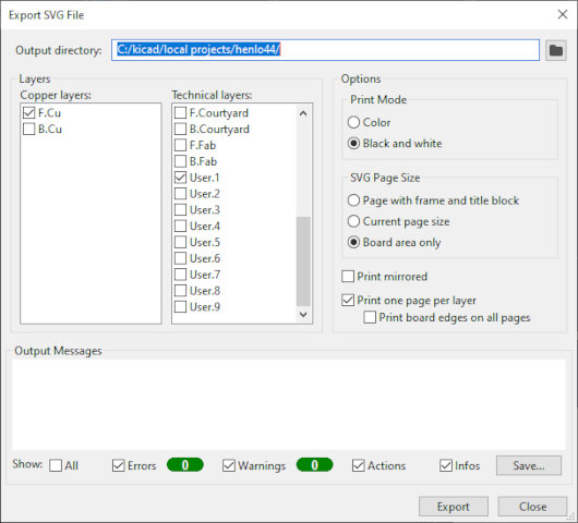
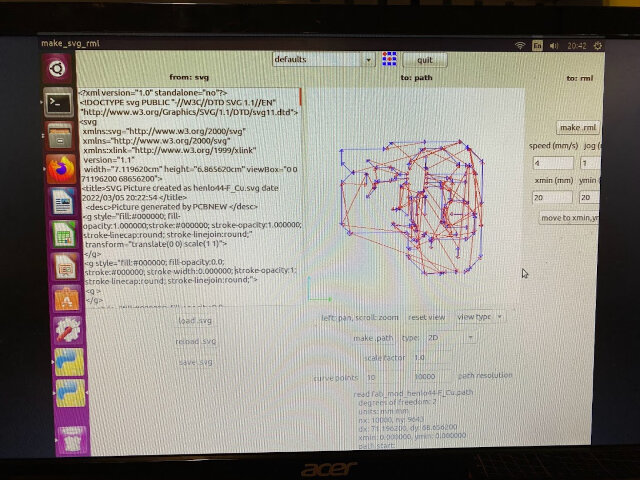
Export as SVG. Note the settings in my screenshot. Select F.Cu (front copper) and User.1 as layers. These will be exported as two separate .svg files.
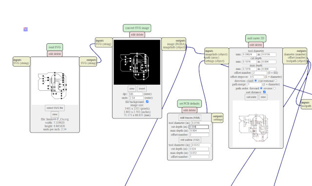
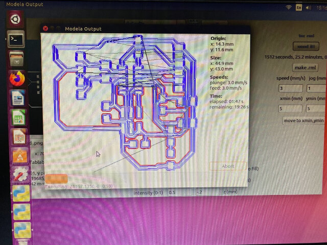
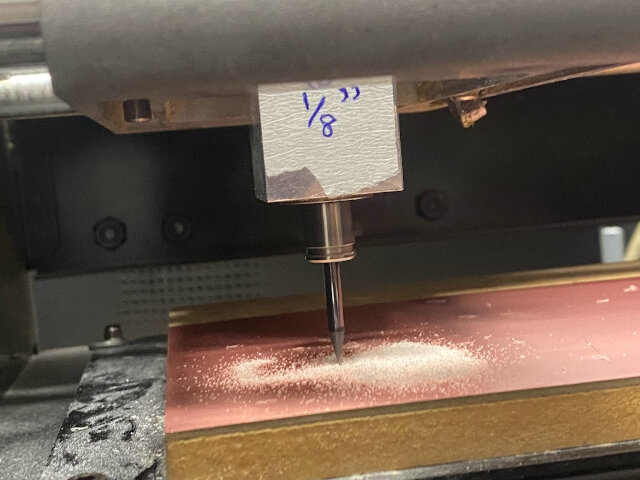
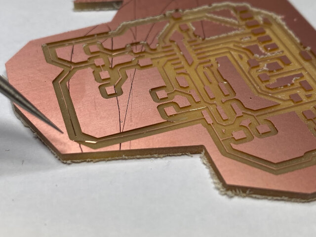
Now take these two .svg files to mods and mill them out!
KiCad also has a 3D viewer in the PCB Editor where you can preview what all the components should like together.
Milling
Confession time, we have been using Fab Modules instead of mods here. Our Roland MDX-20 machine is very old and so is the Ubuntu desktop controlling it. We spent a lot of time upgrading the Ubuntu OS so that it could support running mods but then the connection wouldn’t work with the MDX-20 so we had to downgrade it and return to Fab Modules running locally. Will keep troubleshooting our set up so we can use the newer mods in the future.
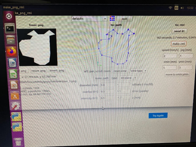
Fab Modules was not taking in .svg files well, jumble of text instead of layout preview like mods.
Since we are always pressed for time, decided to just make the first spiral work and then we can work on getting to the ideal situation later.
Since Fab Modules won’t accept the .svg files for some reason, I used GIMP to convert them to PNG. The first trial went terrible. The low resolution meant the Fab Modules software had a poor output with wobbly right angles.
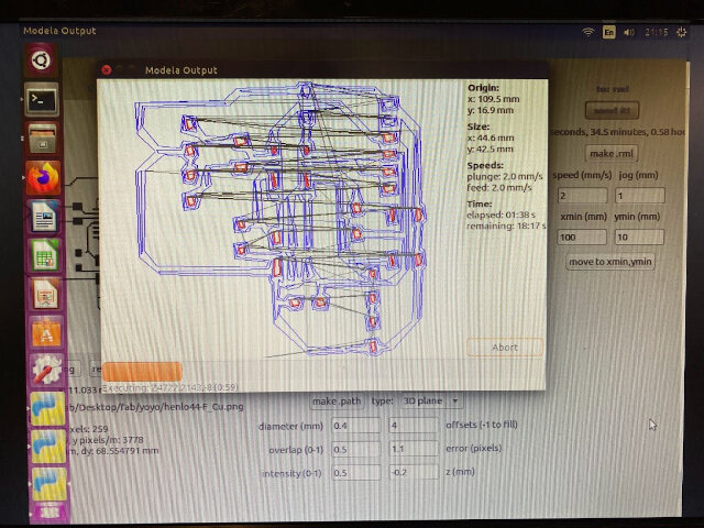
Also I forgot to invert the PNG color so it was cutting out the traces instead of cutting the outline of the traces, heh oops.
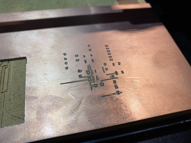
Returned to GIMP and this time changed DPI to 500, which is what the default setting in the mods “convert SVG image” module is, so figured this would also be more acceptable for Fab Modules. Also remembered to invert the PNG colors in Fab Modules this time. Remember: Light is up, dark is down! The traces we want to be the upper layer, so it should be white in the preview.
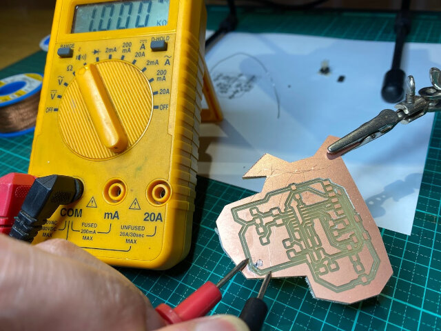
Programming
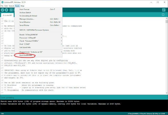
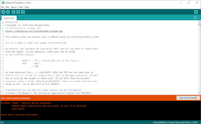
This was really hard. Struggled a long time with USBasp programmer burning bootloader onto new board (unfinished from Week 4). It showed a successful burn in Git Bash with avrdude but afterwards when connecting directly to computer
avrdude doesn’t list atmel ICE as a programmer Couldn’t get target board to initialize through Git Bash avrdude commands.
Switched to arduino as ISP
capacitor
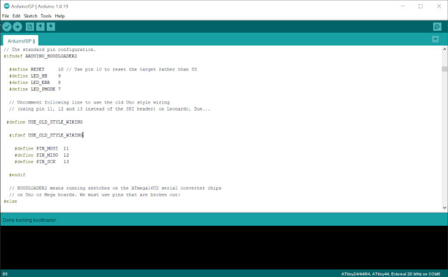
external clock 20MHz
Load firmware/bootloader
(https://www.instructables.com/Program-an-ATtiny44458485-with-Arduino/)
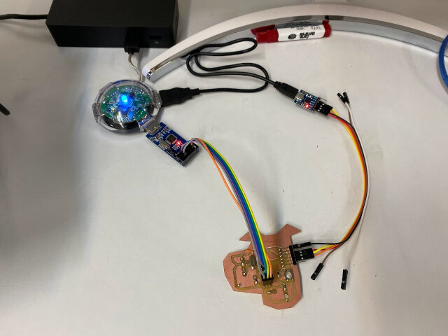
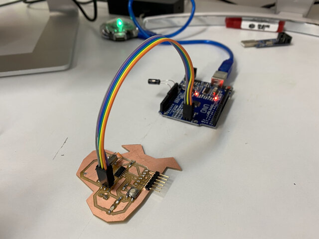
Tried using USB to UART board (converter) to connect to henlo board directly via FTDI
Could not get arduino IDE to flash blink program
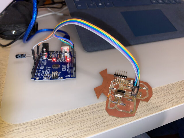
Went back to Arduino as ISP connection
Flashed blink program
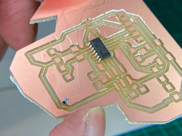
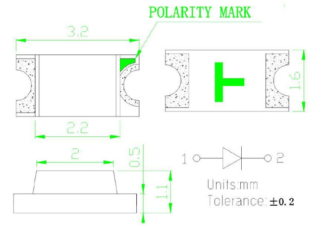
Debugging First step found out I had connected the LED in the wrong direction (when soldering, thought the line at the back was towards the cathode end).
// insert screenshot of smd led polarity indicator
Second error was in my code. Mistook physical pin number for pinout number, had led = 10 when it should have been led = 3. After flashing with correct pin number, it finally worked!
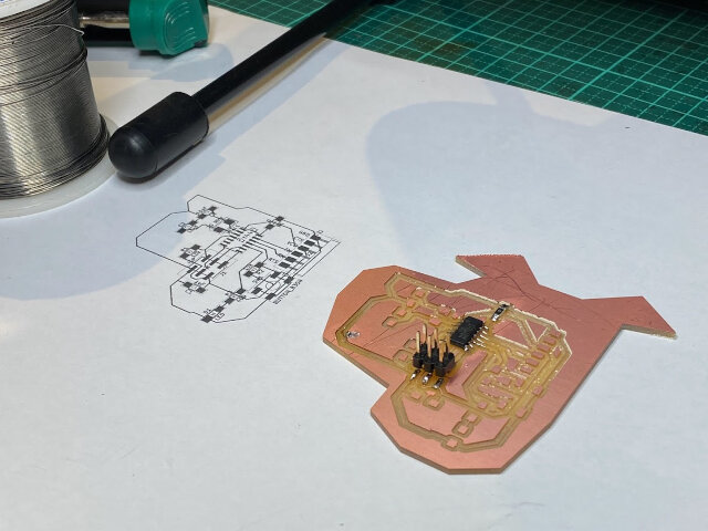
Next to flash Neil’s echo hello world program. For ATtiny44, there was no .ino file to put into arduino IDE directly… and flash via ISP and arduino IDE
So had to go back to Git Bash and do it in command line with avrdude
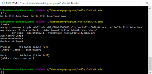
Used avrdude to make .hex file from .c and .make file. rename .make file to “Makefile” avrdude run ‘make’.
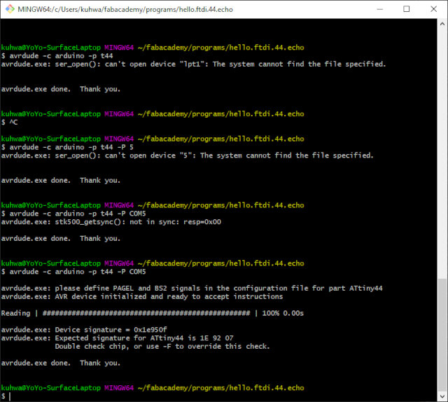
Lots of errors getting arduino to connect
add -P COM5 to specify to avrdude which port to find device in. (this changes, so check with COM port the arduino is connected to in Device Manager each time).
Some more errors
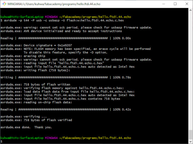
Went back to USBasp, more errors until read cba tutorial add ‘-P usb’ to the command and it worked. Flashed echo hello program onto my new board.
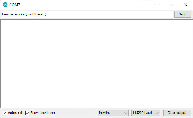
Now to make it echo back “hello” when talking to it through a terminal.
For this part need to install more software environment.
FTDI USB Drivers py serial, term.py?
http://fab.cba.mit.edu/classes/863.13/tutorials/EmbeddedProgramming/echo.html
Lessons learned / Notes for future boards
- don’t need to ride the edge when it comes to design rules. 10 mils works but could be more robust, thicker traces, for safety factor.
- We have resonators with built-in capacitors (SMD) in stock now, don’t need to use through hole + capacitors setup anymore. Replace with one SMD.
- Don’t assume you know device markings from past, always check when in doubt. Case in point: LED SMD line is actually towards anode side.
To-do / Future Work
- install BOM (https://github.com/openscopeproject/InteractiveHtmlBom)
- Try out Fusion 360 EDA (formerly Eagle)
- Try out TinkerCAD (curious about kids’ STEM education)
- Try falsted circuit simulator
- Experiment with SVG-PCB
Conclusion
Electronics are all around us, and this week
Useful links
Design Files
- Henlo44 schematic
- Henlo44 PCB