4. Electronics Production
Group assignment
- Characterize the design rules for your in-house PCB production process
- Document feeds, speeds, plunge rate, depth of cut (traces and outline) and tooling
- Extra credit: send a PCB out to a board house
Individual assignment
- Make an in-circuit programmer that includes a microcontroller:
- Extra credit: customize the design
- Mill and stuff the PCB
- Test it to verify that it works
- Extra credit: try other PCB processes
Learning outcomes
- Described the process of milling, stuffing, de-bugging and programming
- Demonstrate correct workflows and identify areas for improvement if required
Introduction and Set Up
For full description of our PCB production process characterization please refer to our group assignment page.
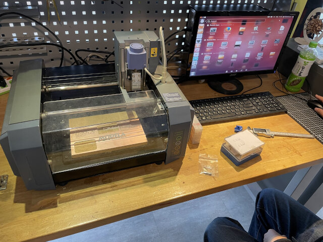
The “mini mill” machine we have for in-house PCB production is the Roland Modela MDX-20. It is connected to a dedicated desktop running Ubuntu OS and running mods CAM to control the mill through a RS-232 connection.
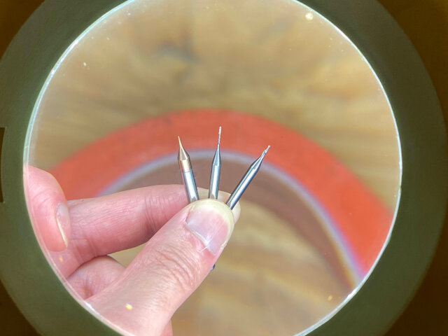
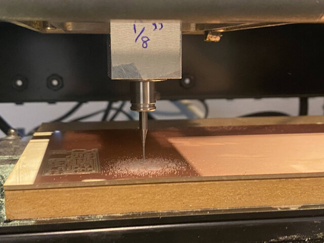
We have a few choices of end mills with various cutting widths: 0.3mm, 0.6mm, 1/64”(from left to right).
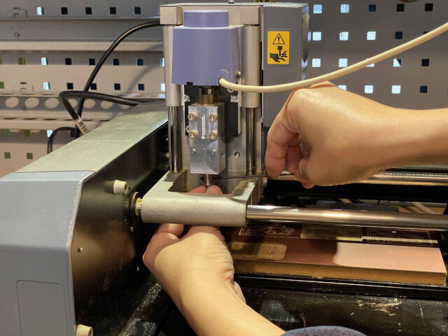
Load end mill into collet and secure with small allen wrench.
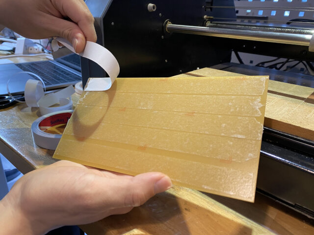
Using double-sided tape is best to hold down the PCB blanks. Clamps can result in an arch in the middle, which creates an uneven z-plane when milling.
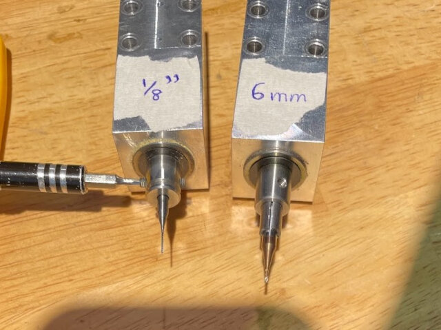
We have three sizes of spindles available for the machine here:
- 3mm
- 6mm
- 1/8”
These sizes refer to the shaft diameter of the end mills (like drill bits, but made for cutting horizontally) that the spindle hole is designed to hold.
3mm end mills are no longer readily available and most of the ones we had are now broken.
4mm end mills can be found cheaply here in Taiwan but we did not have a spindle for that size. The Roland MDX-20 is a pretty old model, so finding one would be difficult. Even if it were available, these spindles are expensive ($300+ USD). Therefore the most practical solution was to get an adapter so a 4mm end mill could fit in a bigger spindle. We acquired a 6mm -> 4mm adapter collet so we couuld use the 6mm spindle with them, but unfortunately when we tried it out it was too tight, causing the 4mm end mills to not be able to set in fully. The tip extended quite far from the spindle and this relatively long length made it more difficult to support forces on the end mill horizontally and so the heads broke off easily when trying this solution.
Fortunately, we still had a few 1/8” end mills in stock. We had to be careful to not break them before finishing our assignments this week otherwise we’d really be out of luck.
More 1/8” end mills were ordered and being imported from the US, the great land of imperial measurement.
Using MODS
Mods is a CAM developed by Prof. Niel at MIT Center for Bits and Atoms. The idea is to be a universal CAM to control all sorts of machines for mass digital fab democratization in the future.
Import PNG file of circuit board into mods. Enter parameters and generate toolpath (G-code) for Roland MDX-20.
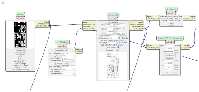
Resulting toolpath generated.
MDX-20 cutting settings
We found these settings to work best, not pushing too much and preserve the end mills from breaking, but also not extremely slow. The settings below should be used at Fablab Taipei instead of default Mods settings.
Milling traces settings
Select “Mill out traces” in dropdown menu. Should default to cutting out “3D Plane” mode.
Tool diameter 0.4mm
Cut depth 0.1
Speed 3
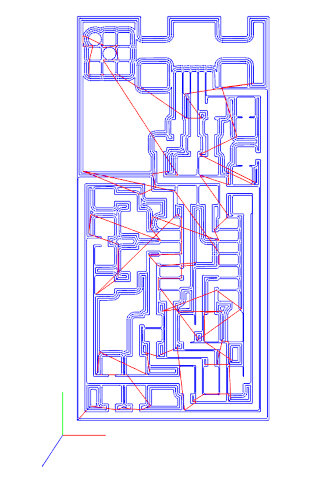
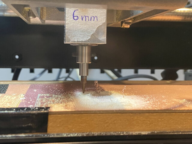
Milling outline (cut out board)
Select “Cut out board” in dropdown menu. Should default to “3D Rough” mode.
Tool diameter 0.6mm
Cut depth 1.7
Speed 1
Note: Usually 1/32” end mill is used for cutting out boards (0.79mm) but we don’t have those here. For cutting out we use the larger 0.6mm end mills we have.
Milling test comb
Milling test comb please see group assignment page.
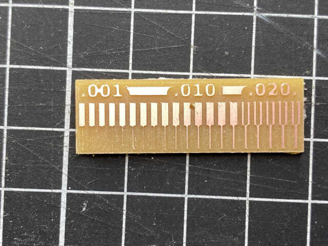
From this test we know that the small trace that our machine can cut is 10 mils (thousandth of an inch). The smallest gap width in can cut is 0.4mm (width of 1/64” end mill).
ISP programmer - FabISP
Okay cool, so we’ve been talking about how to use a mini mill to produce in-house PCBs, but WHAT are we building exactly this week??
We’re building a FabISP, which is an ISP programmer. Basically we burn a firmware onto this PCB, so it can be used to program other new PCBs, including burning bootloaders on to them so the new PCBs can be programmed without a programmer through other means like FTDI.
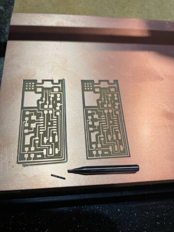
This is one of the PCB designs provided to us by Neil. In future weeks we will design our own boards but for now, we’re just familiarizing ourselves with the milling and stuffing process.
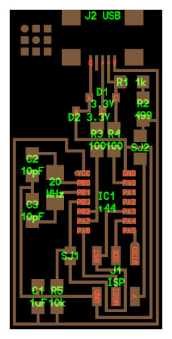
FabISP based on ATtiny44
Now time to start milling out PCBs for the week!
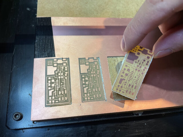
Milling FabISP Programmer
Start with cutting out traces with 1/64” end mill.
First trace cuts were fine but then the cutting out board step messed up. Speed set too high and the end mill broke. Reduced speed for second try.
Comparison of spindle, collet, end mill set ups. Left is for milling traces, right is for cutting out board outlines.
Cutting out second board.
Second board also failed. Third time’s the charm!
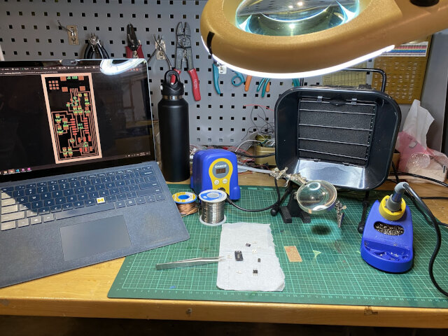
Stuffing the board
“Stuffing” means attaching the electronic components onto the board.
There are two ways we can do it at Fablab Taipei.
- Soldering iron
- Reflow soldering
We will start with soldering by hand first.
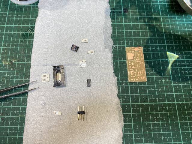
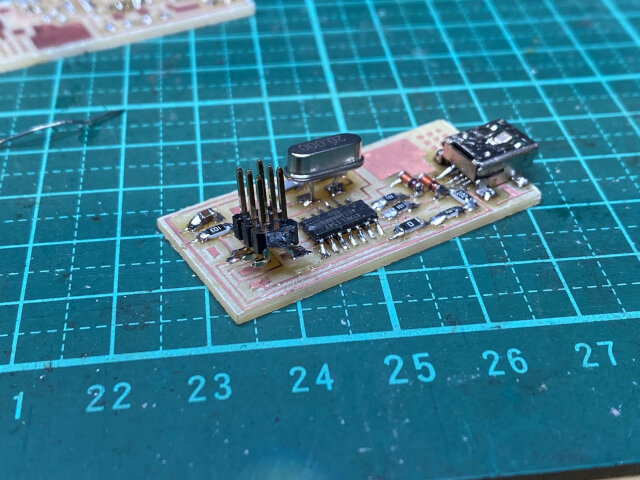
The components needed for the FabISP are:
| Qty. | Component | Marking(s) |
|---|---|---|
| 1 | ATtiny44 | ICt44 |
| 1 | 6-Pin Header | J1 ISP |
| 1 | USB Mini-B SMD Connector | J2 USB |
| 1 | Crystal 20 MHz | 20 MHz |
| 1 | Capacitor 1uF | C1 |
| 2 | Capacitor 10pF | C2, C3 |
| 2 | Diode Zener 3.3V | D1, D2 |
| 1 | Resistor 1k ohm | R1 |
| 1 | Resistor 499 ohm | R2 |
| 2 | Resistor 100 ohm | R3, R4 |
| 1 | Resistor 10k ohm | R5 |
| 1 | Resistor 0 ohm | SJ2 |
The setup:
- soldering iron with brass cleaning cushion thing
- exhaust fan for smoke fumes
- solder
- copper wick for the inevitable mistakes
- tweezers for picking and placing tiny components
- milled empty circuit board
- components arranged neatly on tissue
- lamp with magnification glass
- laptop showing PCB layout
Components arranged roughly in the regions they will be soldered in. In general, it’s better to work from more inner in the board to outside, so placed components don’t block you as much as you go.
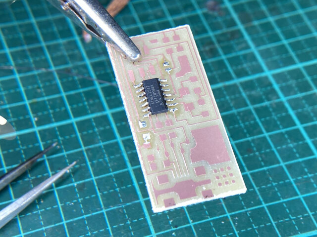
Started off strong, MCU attached and pin solder joints looking not bad.
Major uh oh’s.
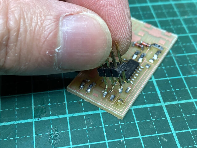
Ugh why was I so OCD about getting the pin headers on super straight… ripped out the trace pads for the header pins accidentally and now I have to redo everything because not enough trace left to salvage it…
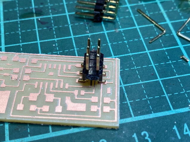
My first attempt I rushed with janky straight header pins bent using pliers. This made a very uneven attaching surface. Later found out L pins can be pulled out and reversed in the black plastic holder bit. This makes it a lot flatter and easier to solder onto the PCB.
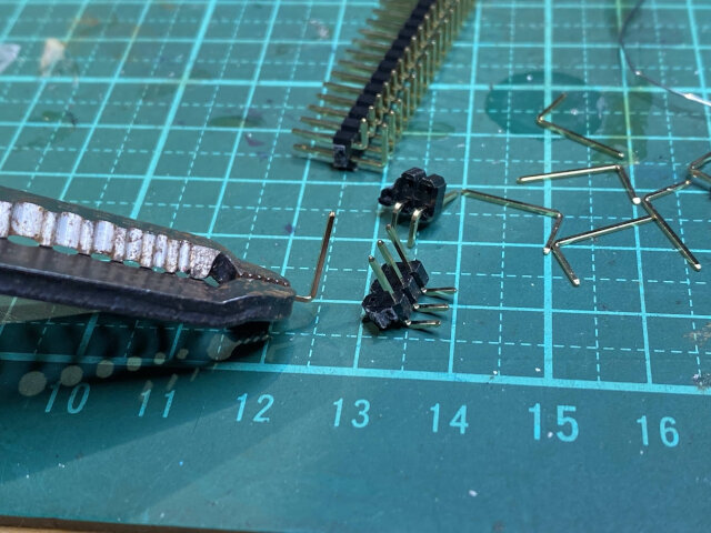
Comparison of jank vs pull-out-and-reverse.
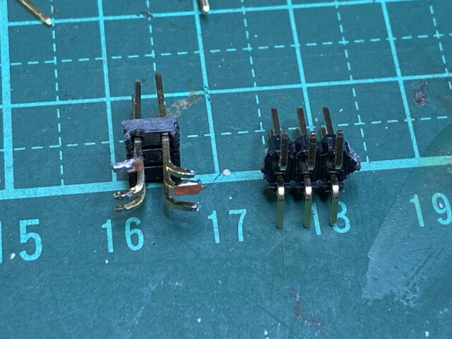
Cut short to fit on the trace pads. Sits much nicer and flatter than the janky hand plier bent one for sure.
Omg I did it again…
But this time it’s salvagable with some extra solder.
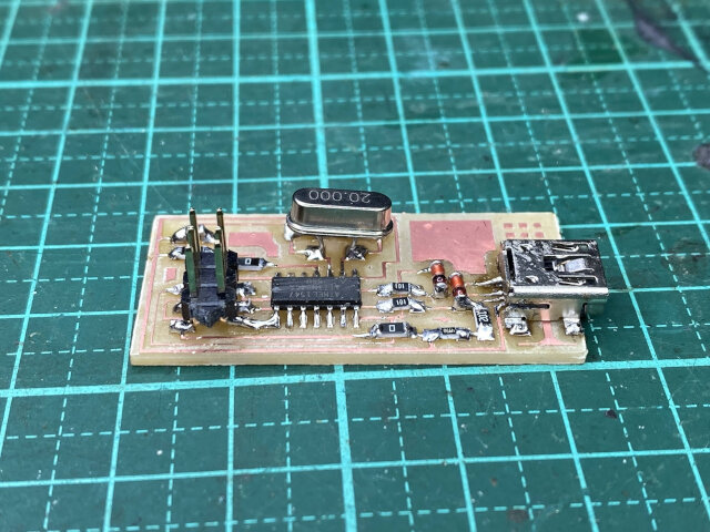
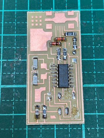
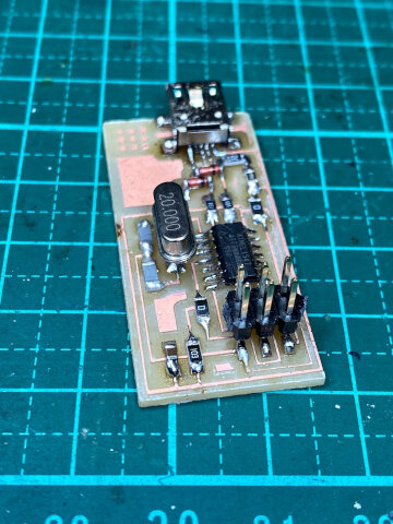
Done!
Smoke test
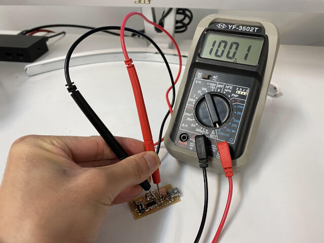
First plugged in FabISP via USB directly to my laptop (later learned that’s kinda risky haha oops) and fortunately no error messages! Means there’s at least no short circuits in regards to power supply.
Quality Check
Tested each line for continuity from beginning to end. Like V from USB pin to V in the 6 pin.
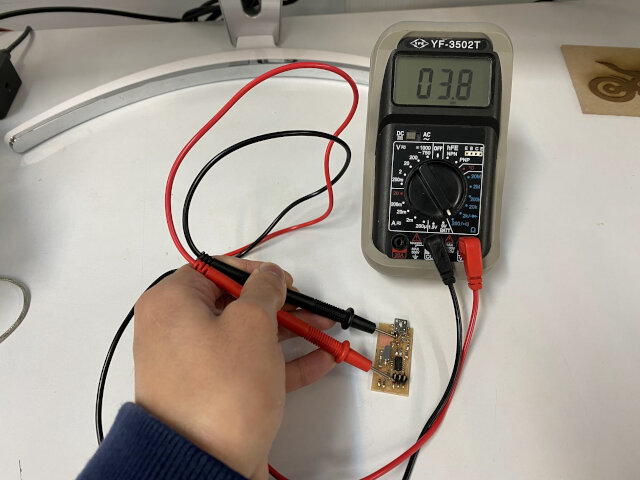
Measure values across resistors to make sure they’re working properly and within specified value. This resistor in the picture below is a 100 Ohm resistor.
No problems!
*Note: later learned continuity tests like this are not that useful after the board is stuffed because there could be other factors.
Programming
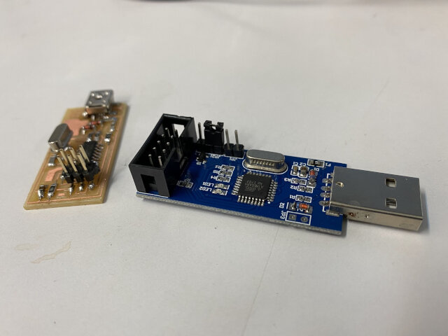
Now the hardware is complete, we move onto the software part. For this we use another programmer board (USBasp) to program the FabISP.
Burning bootloader
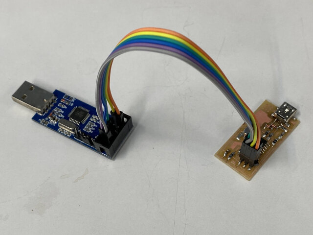
USBasp is an open source USB in-circuit programmer for Atmel AVR controllers. It has a 10 pin header (the additional pins are all ground) so we need to connect it one pin at a time to our FabISP board with only 6 pin input.
Pin match up.
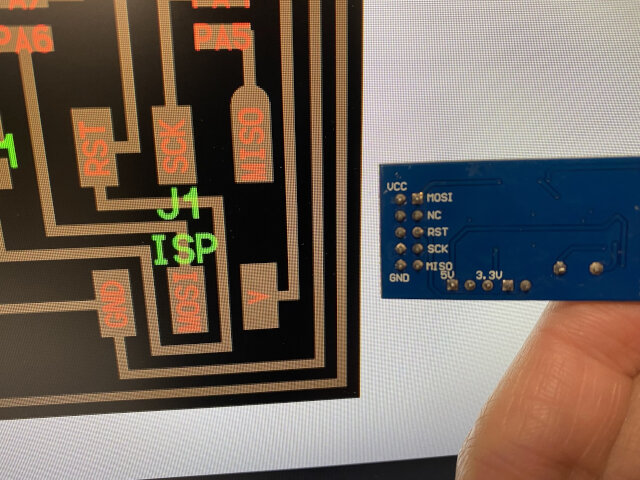
Proper connection of USBasp to FabISP’s ISP pins.
Software environment
First install AVRdude https://github.com/avrdudes/avrdude/
Supposedly it should be already installed with Arduino IDE but upon checking in PowerShell terminal, it is not on my computer. So install from github and add to PATH so it can run on terminal from anywhere.
Download firmware package for USBasp https://www.fischl.de/usbasp/
Install USB driver for windows, so FabISP can be configured properly as a lib-win32 device. http://zadig.akeo.ie/
Conclusion
Ultimately after much troubleshooting and debugging, I could not get this FabISP to work correctly as a programmer this week.
However, I finished this assignment in Week 6!
Useful Links
- 3 digit SMD resistor codes
- 4 digit SMD resistor codes
- Diode polarity
- Surface Mount Soldering 101 video
- How to remove a surface mounted chip with only a soldering iron
- USBasp website
- FabISP Progamming tutorial
- FabTinyISP tutorial
- Using the GNU AVR toolchain on Windows 10