Week 04: Electronics production
Assignments:
-
Group assignment: Characterize the design rules for your PCB production process: document feeds, speeds, plunge rate, depth of cut (traces and outline) and tooling. Document your work (in a group or individually).
-
Individual assignment: Make an in-circuit programmer by milling and stuffing the PCB, test it, then optionally try other PCB fabrication process.
What to learn:
-
Described the process of milling, stuffing, de-bugging and programming
-
Demonstrate correct workflows and identify areas for improvement if required
Have you?
-
Linked to the group assignment page
-
Documented how you made (mill, stuff, solder) the board
-
Documented that your board is functional
-
Explained any problems and how you fixed them
-
Included a ‘hero shot’ of your board
DOUBT: Does the in-circuit programmer need to work to complete the assignment? Answer: Yes. Your board must be recognized by the host computer and it must be able to communicate with the target board.
DOUBT: Do I have to include NC-files? Answer: No.
Steps of this week assignment:
ELECTRONICS INTRO 18.02.2021
Today we went to the FabLab and Henk did an introduction on how to mill boards for electronics, how to solder them and the basics of the material and machines used.
PCB: printed circuit boards
ISP (in-system-program): chip programmer to program ICs like AT tinys for example.
IC: there are different types of IC: AT tiny (45), AT MEGA, …

You use the IC to program the board:
FTDI: talks in very ancient communication protocol (serial communication) one pin is sending info, one pin is receiving information, one for ground and one for vcc (power source). In order to communicate you need the FTDI.
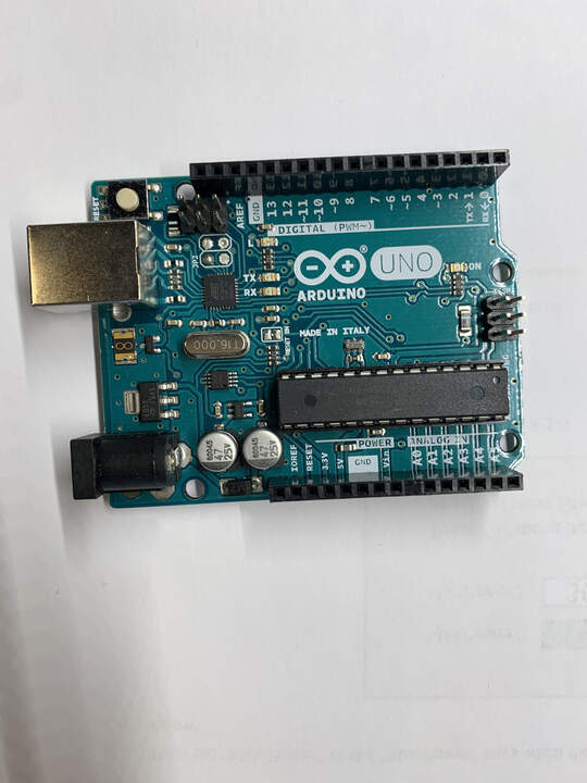
Arduino board
UPDI: instead of an ISP you use a UPDI (this one has only two pins). FTDI and UPDI use USB to communicate serial through the microprocessor (serial communication).
The three things we can produce this week will be ISP/UPDI/JTAG programmers.
ABOUT THE MACHINE:
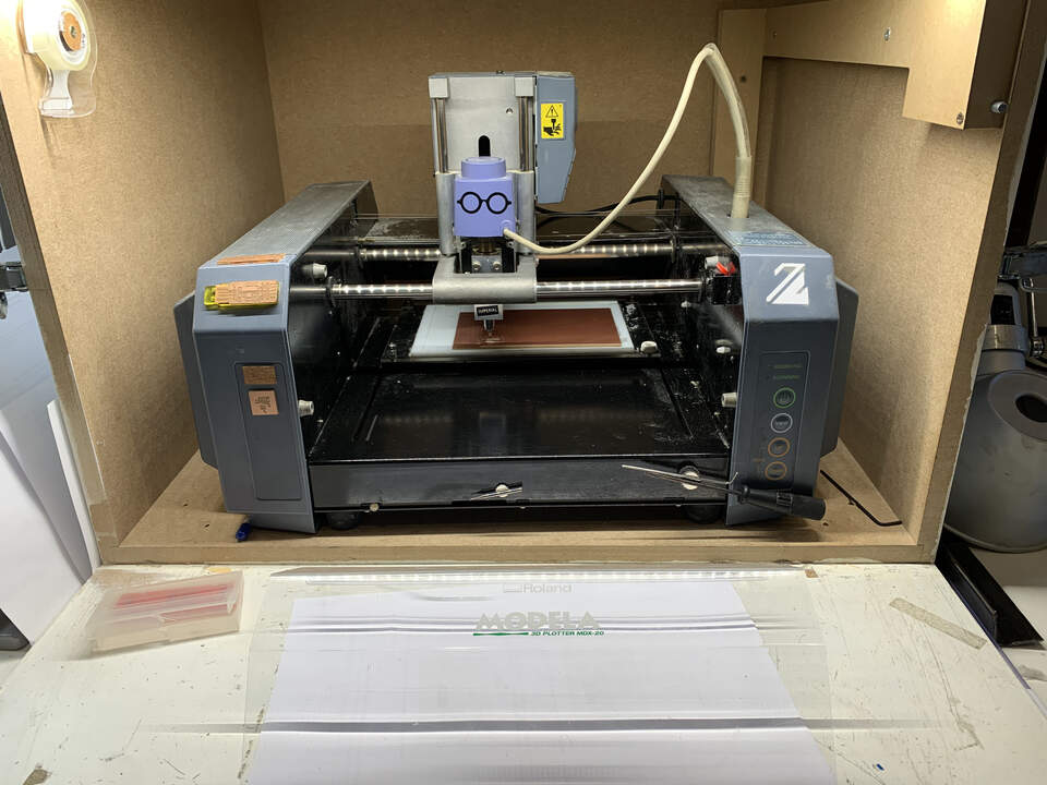
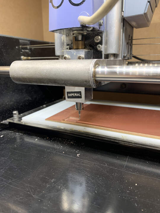
At our Fablab we have a Roland Model MBX. This is a small milling precision machine. CNC stands for Computer numerical control and milling is a process that is quite similar to drilling or cutting. It uses a cylindrical cutting tool that can rotate in various directions, moving along multiple axes and creating different shapes, slots, holes and impressions.
-
The machine has an accuracy of 0.002mm + milling bit (but you never gonna get that because it is mechanical you will have to adjust it, depends on the gears of the machine and how you are going to operate the gears)
-
it has a x(drill), y(plate) and z axis(drill)
-
for the traces we use 0,4.mm mill and for the cutting out we use 0,8 mm
ABOUT THE SOFTWARE
You operate it through mods. If you enter the terminal and enter the command:
mods
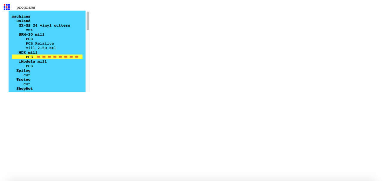
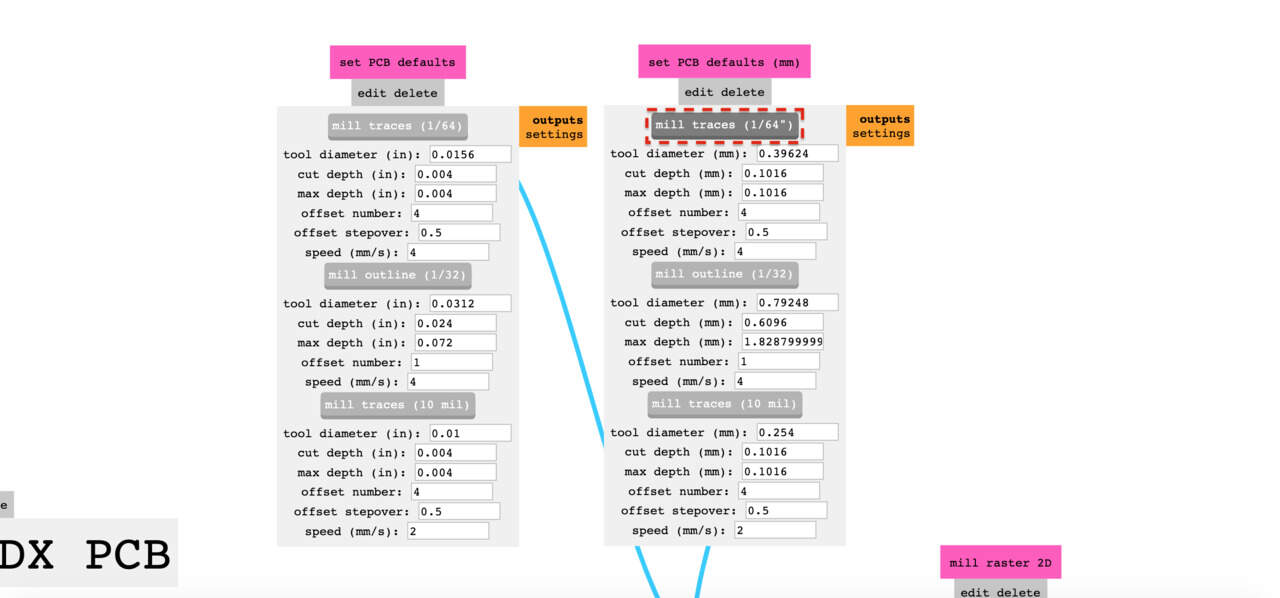
It will open up mods in the browser. Then you go to programs > open program > mdx mill > PCB
-
In Mods you can either insert svg and png
-
You can access the FabLab circuits list here
-
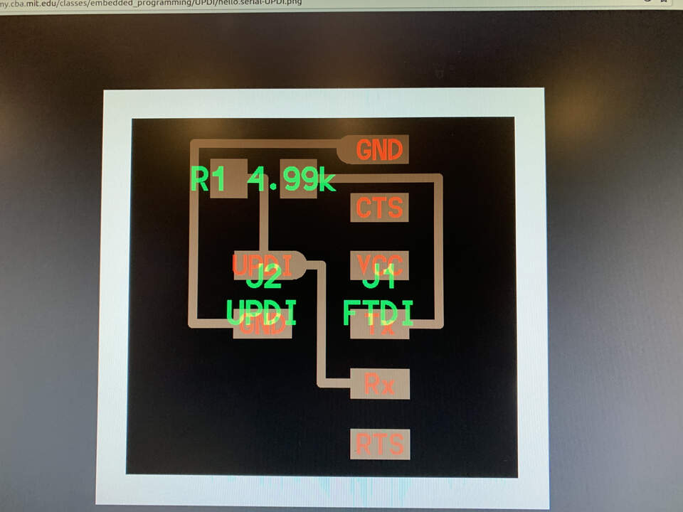
In order to understand the workflow we will choose the first option of UPDI from the three options:
- 1st one is the most simple: changing cables
- 2nd one has a vcc, extra pin with the power on it
- 3rd one you don’t need and external FTDI cable cause it has a chip on it
Henk showed us how to mill the first option of UPDI by giving us the basic parameters and steps we had to insert and follow in Mods in order to mill the traces and outline of our boards. We then repeated this process (which I explain in detail in the group assignment) for the group assignment to characterize the rules for the PCB process.
ATTACHING A NEW COPPER PLATE
When starting a new mill you will have to attach a new copper plate in the machine. The board where you attach your new copper plate has a triple protection:
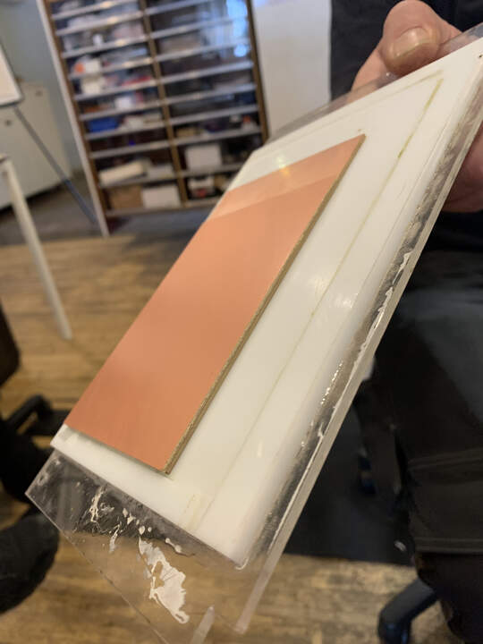
BASE > ACRYLIC(milled border with cnc, completely leveled with machine) > SACRIFICIAL LAYER -> ON TOP MY COPPER PLATE
My new own copper plate will attached to the base by using double sided tape so in order to stick it we have to remove the last one as seen below:
We will also have to remove all the glue from the base so that the new plate is straight (if necessary use sticker remover). When we have the base ready and clean we will fill it with tape to make it as study as possible and attach the new copper plate to it. Insert the whole base to the machine and tighten it with the screws (tight but not too tight).
GROUP ASSIGNMENT: CHARACTERIZE THE RULES FOR THE PCB PROCESS.
MAKING THE TRACES MILLING:
-
From the fab lab circuit list we download the tracing file we will be milling:


-
We open Mods:
-
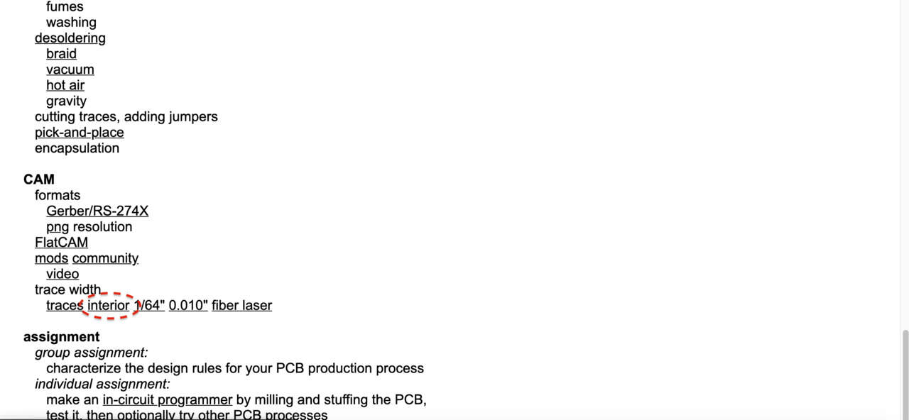
We open the png file in Mods(dpi:1000 almost it needs to have a high dpi because otherwise the pixels are too big):
-
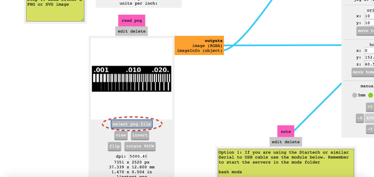
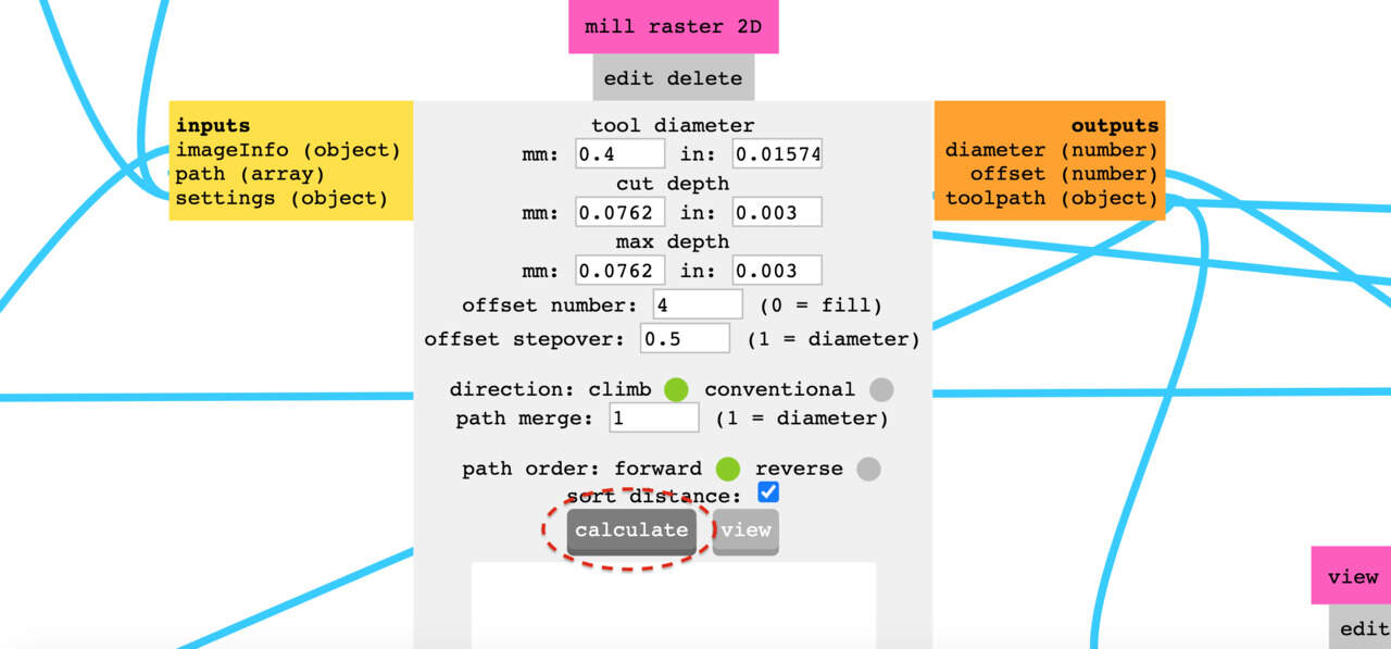
We go to set PCB default and press mill traces, this will feed the the mill raster 2D which has all kind of parameters
-
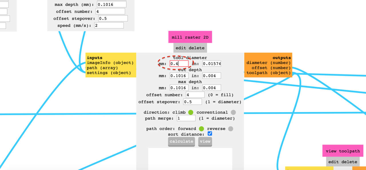
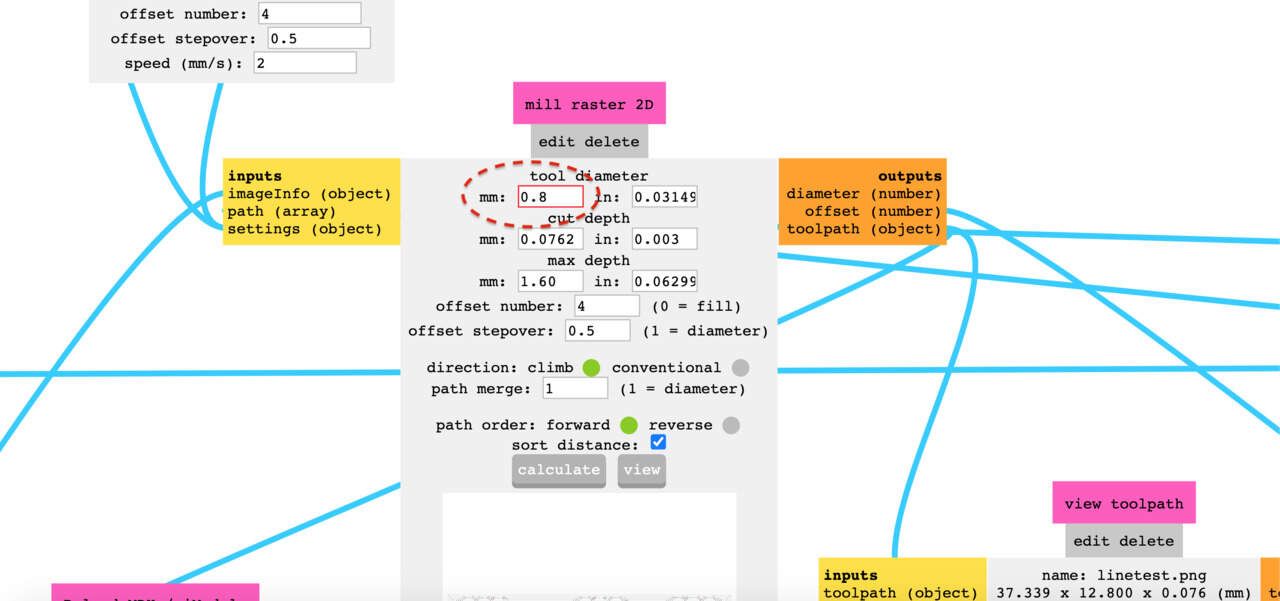
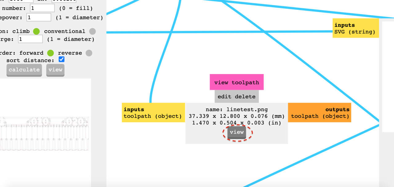
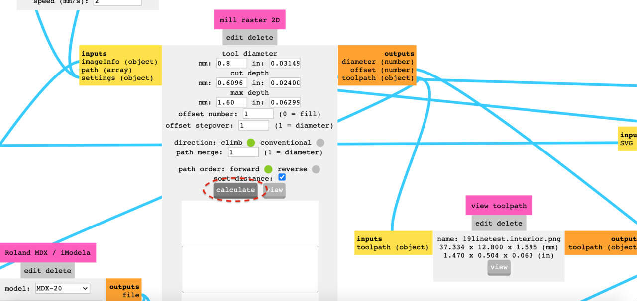
We go to the mill raster 2D and enter the following parameters:
Specify the tool diameter, we will be using a 0,4mm flute endmill.
Specify cut depth: 0.003 inches (0.0762mm)
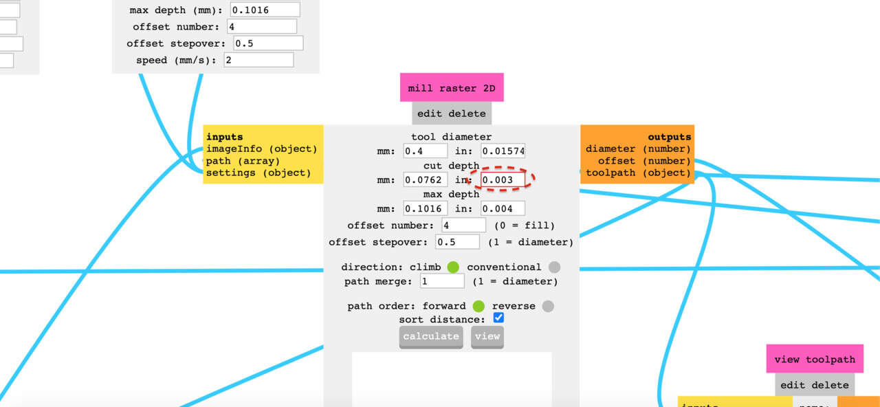
Specify max depth: 0.003 inches
Specify offset (if you change the offset the machine is quicker but it is harder to sold after):
Specify stepover: (it will you will get a nice set in the board)
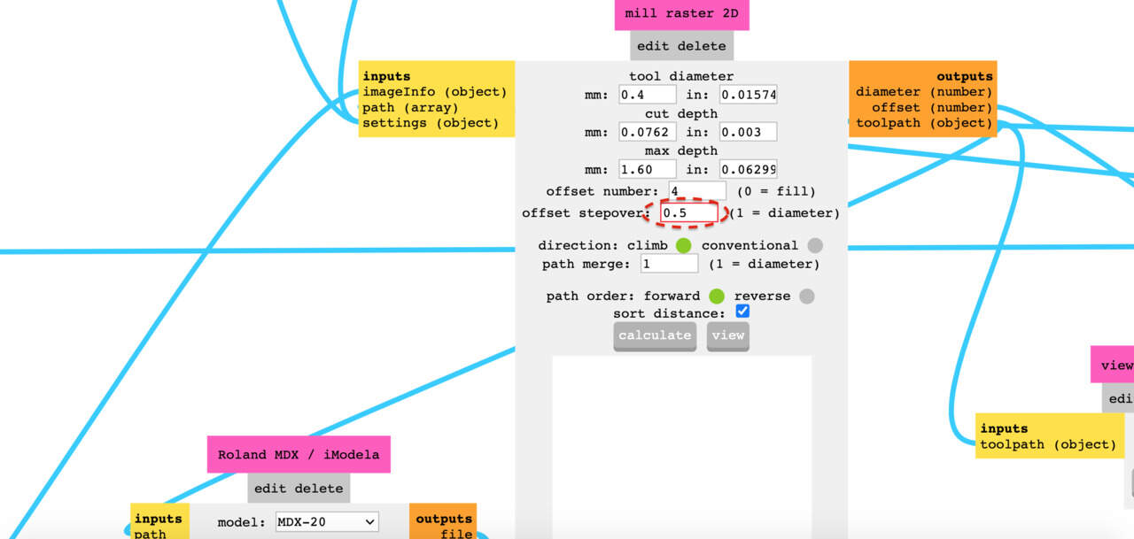
Direction always remains in climb (depending on the direction that the milling goes it will chop material from one side or from the other, so climb will be neater. See differences between climb and conventional here.
Path order: forward (does not really mean anything)
Sort distance has to be ticked.
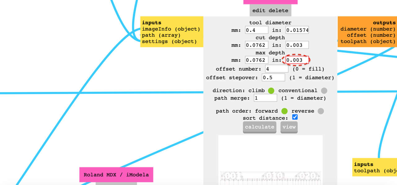
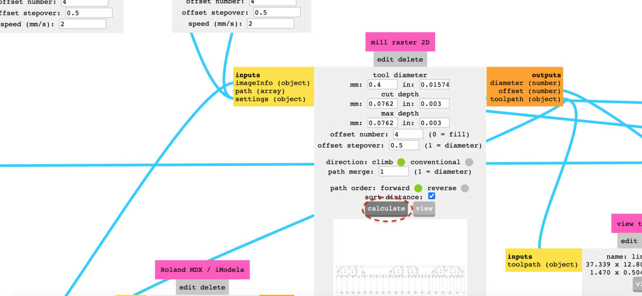
Press calculate (it will calculate what it has to do and translate it in gcode for the machine):
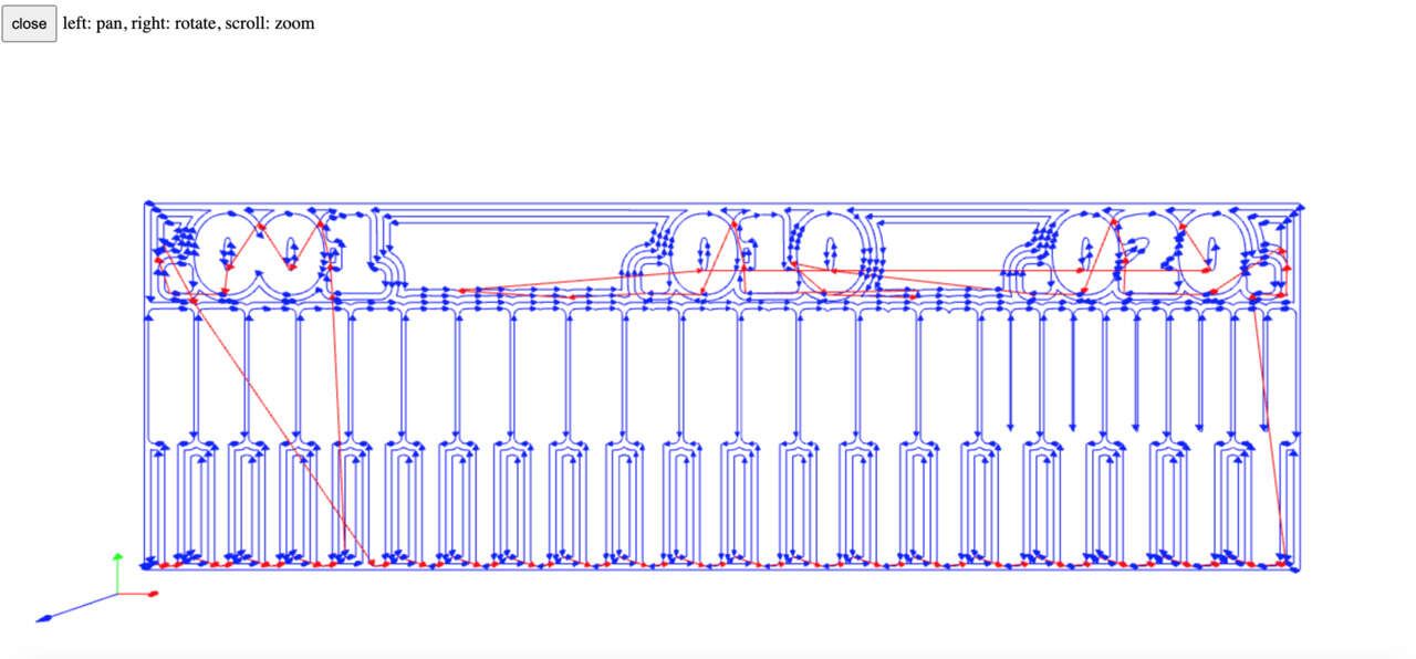
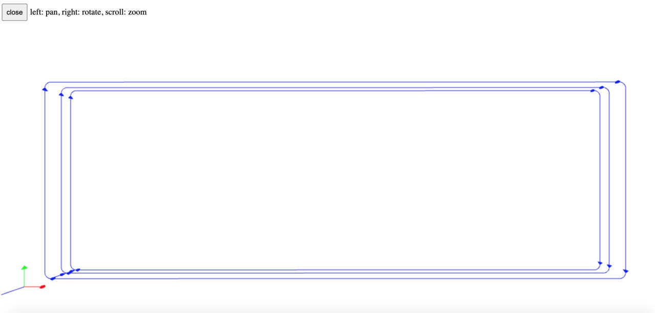
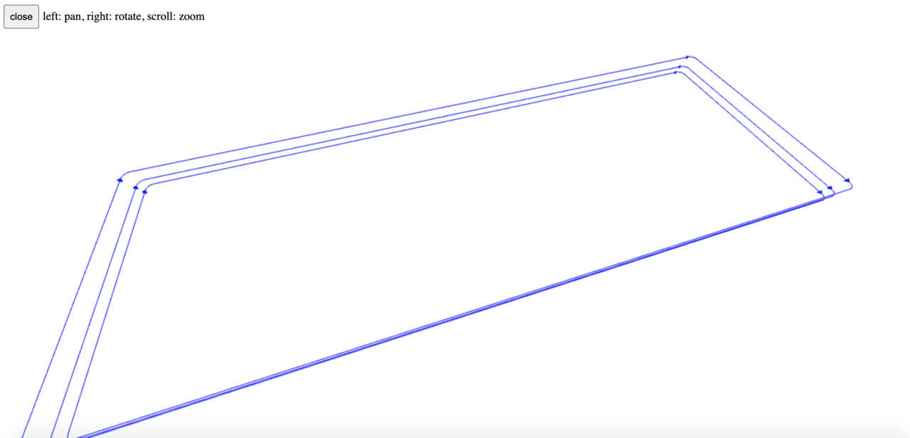
This will automatically open a toolpath viewer where you can see the traces (3D VIEWER)it has 4 lines (default offset). The red lights are the travelling of the machine. You can also use view toolpath > view (window opens) > it is good to open it because sometimes you see design mistakes.
-
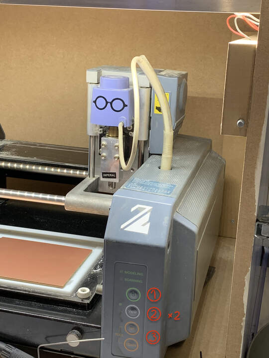
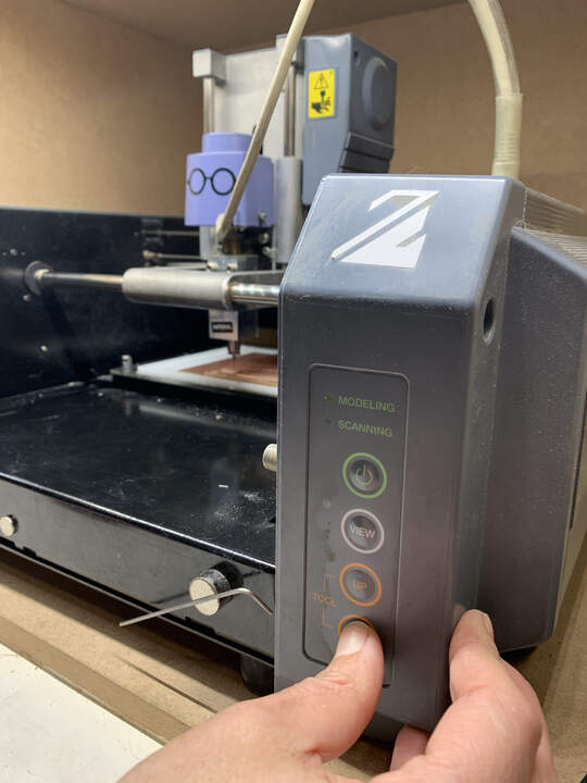
We now turn on the machine with the following buttons: 1: Turn machine on 2: Press View (plate will go back and right) and press view again so that the mill sets up in origin (and we can chane the mill). 3: Press Up/Down buttons to pull mill down.
-
Change mill and put a 0,4mill (for traces)
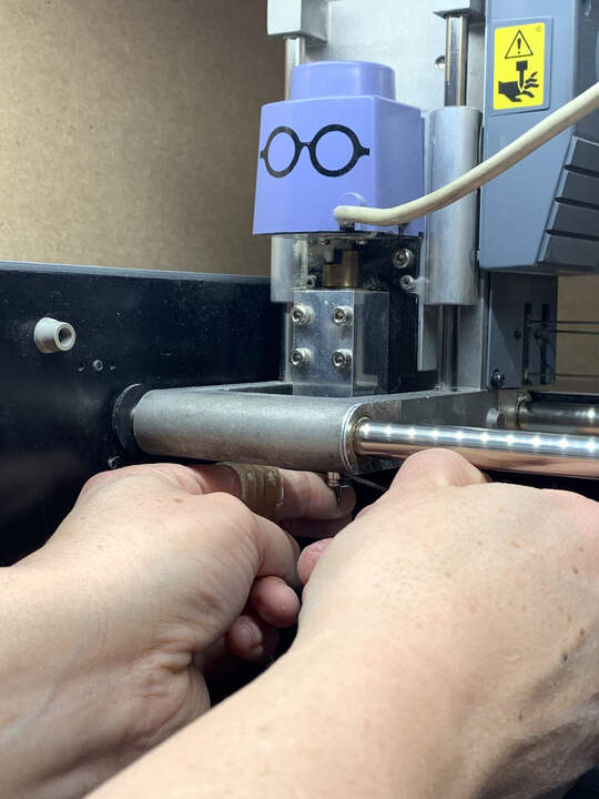
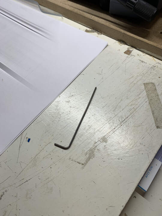
We will unscrew the mill counterclockwise to make the mill loose with an alan key:
We screw the new mill holding it with the two fingers as shown below:
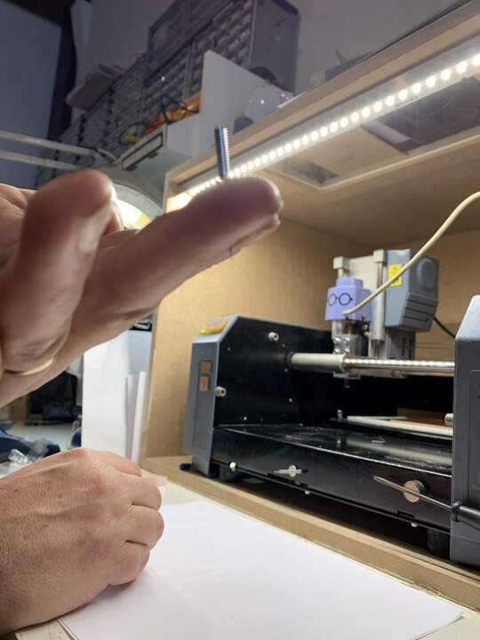
We tighten it clockwise with the alan key:
-
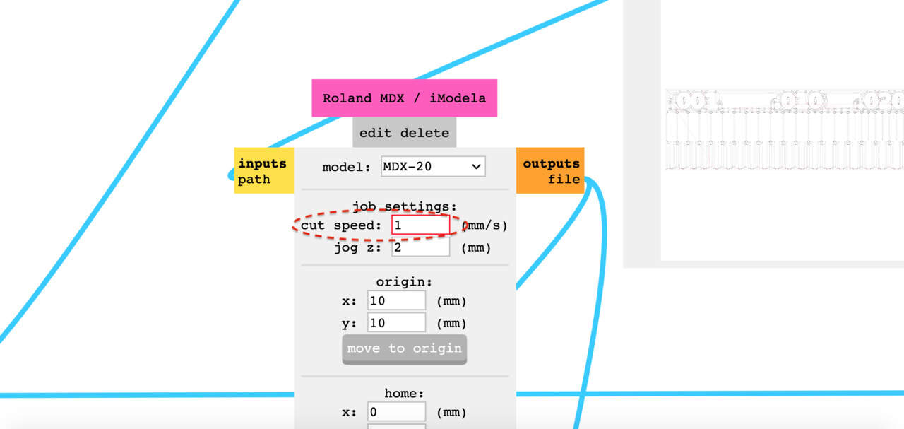
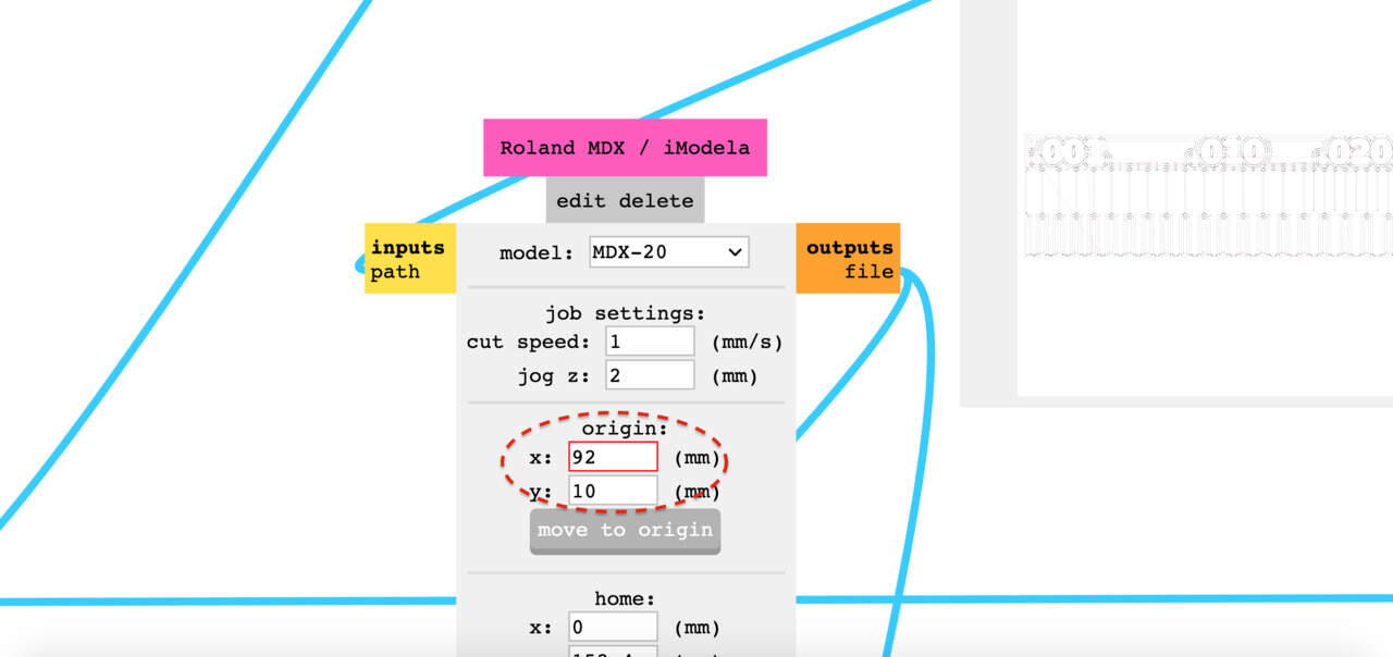
We go back to Mods and we change the cut speed to 1mm/s (VERY IMPORTANT, Henk reduced the speed to to avoid milling bits getting broken all the time):
-
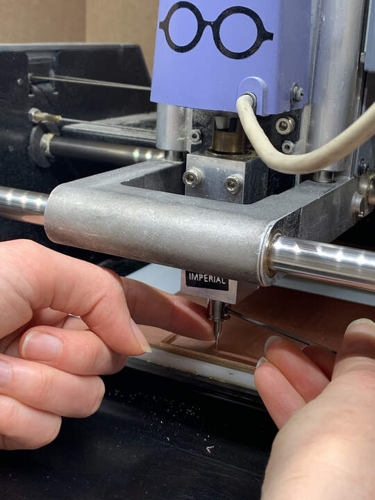
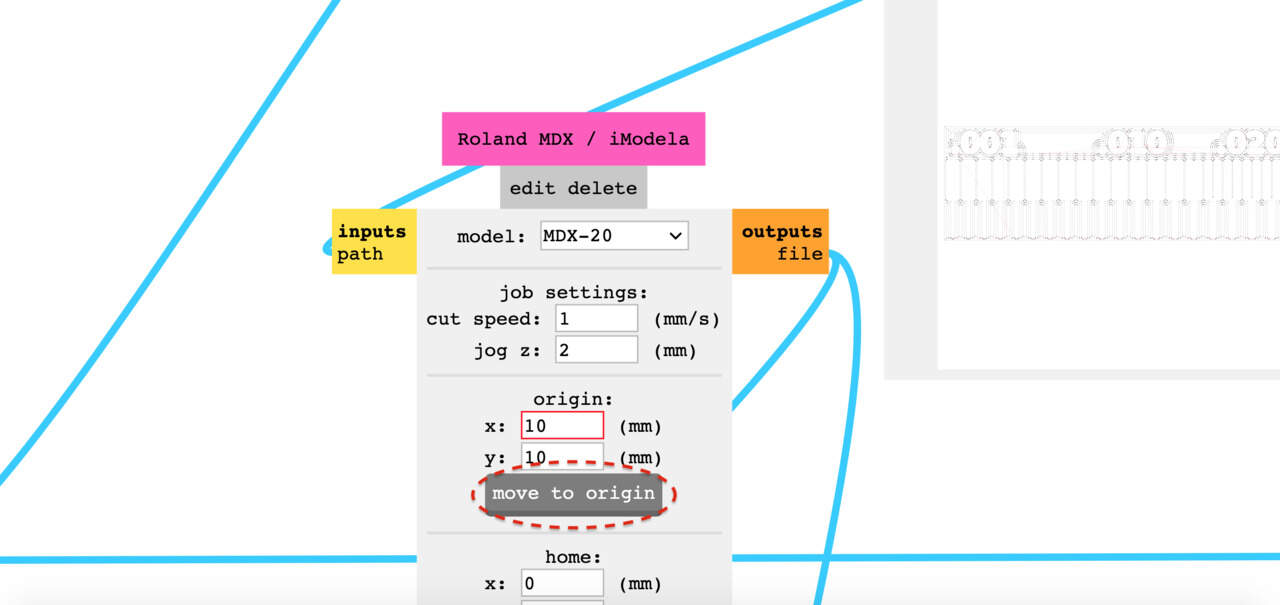
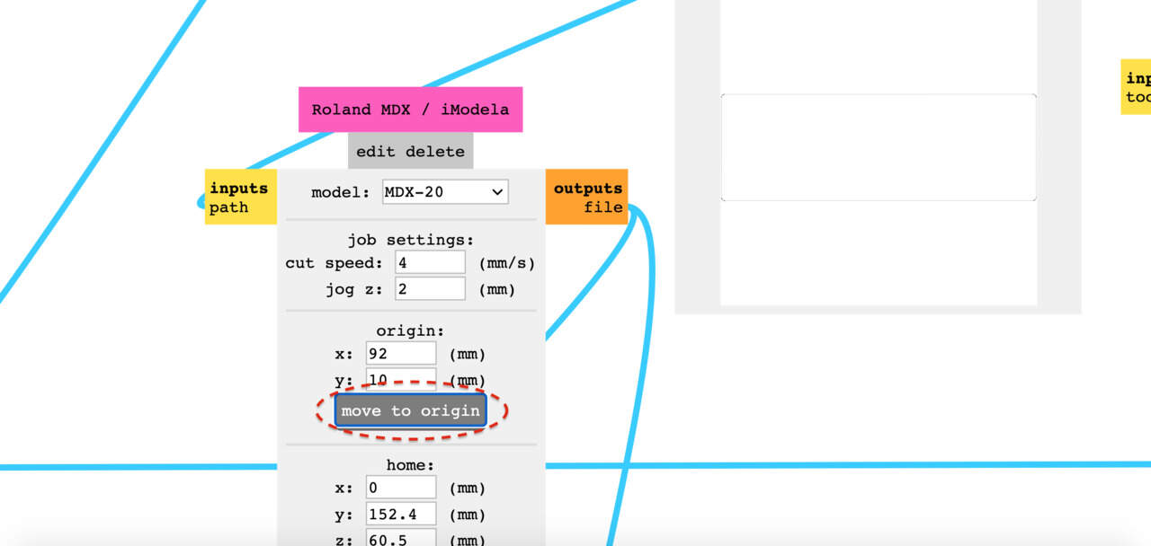
Press move to origin to check where the origin in the machine is placed.
-
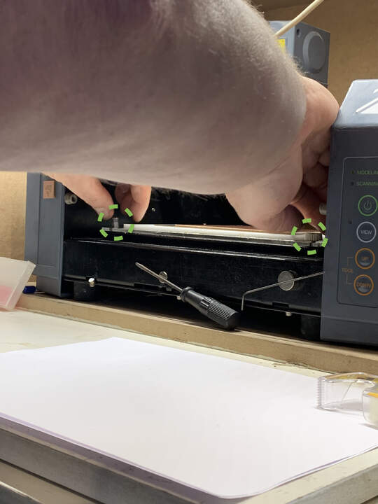
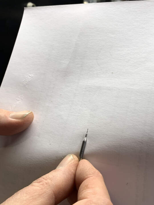
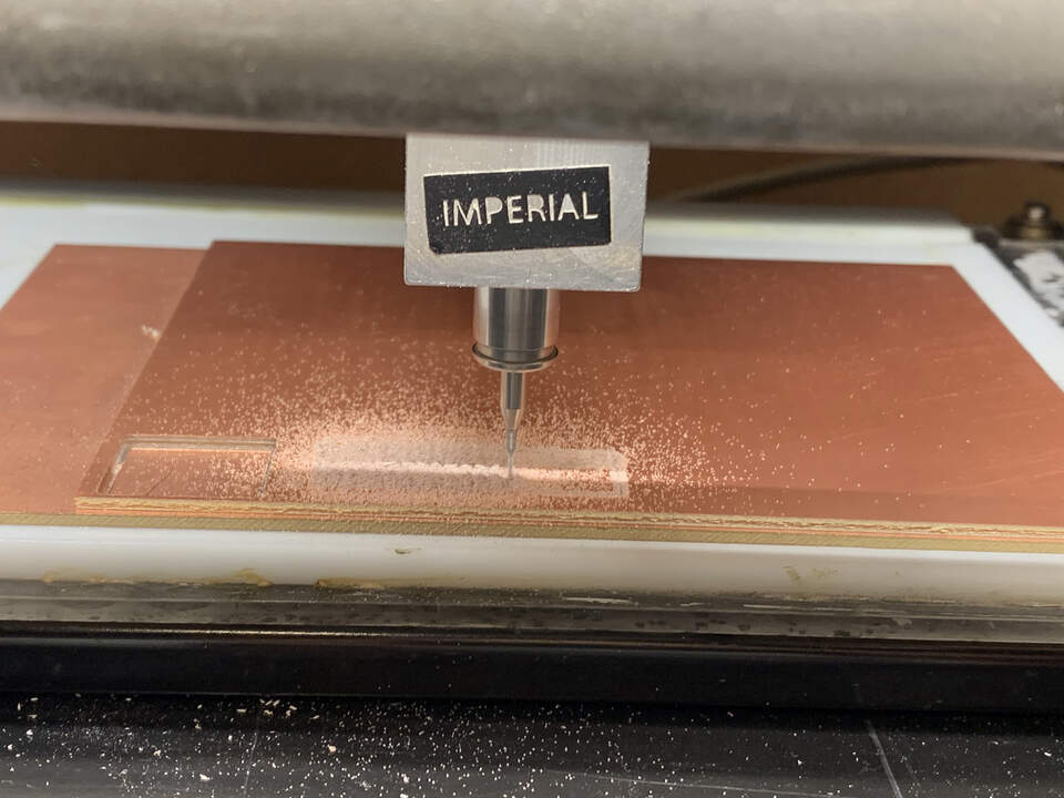
Then we will change x and y so the mill is just above the plate (take a picture of the origin just in case the machine colapses and you have to start again from the same point):
-
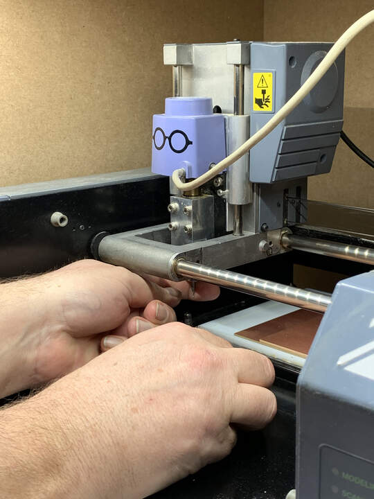
Go to machine and change z axis manually with the alan key just so it touches the board. You should lower it enoigh with the down button so that you mill just stand out less than a cm manually:
-
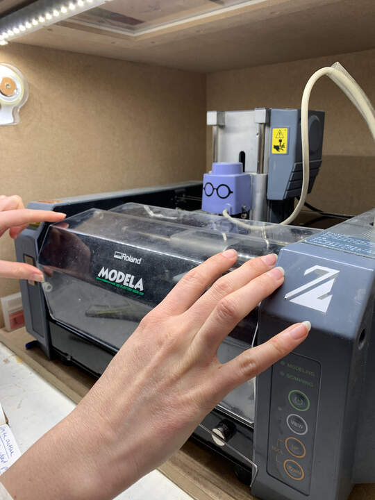
Cover machine with glass:
-
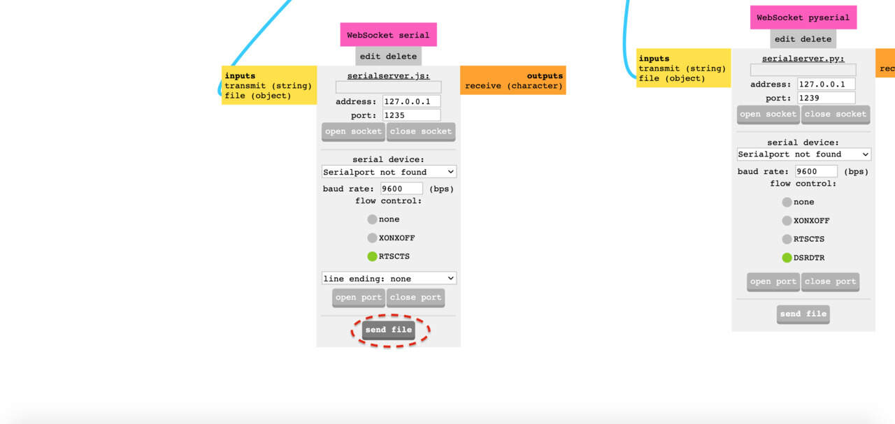
Go to mods and press calculate in mill raster 2D again (always do this before sending file):
-
Press send file so that machine starts milling:
-
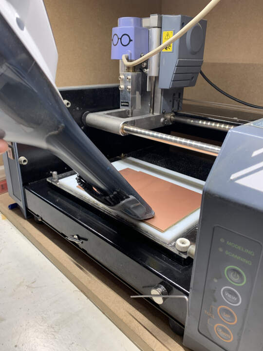
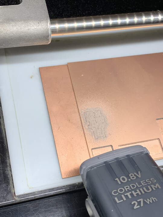
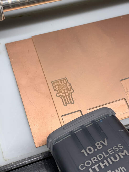
This will start milling the traces (it took around 15 minutes). When finished we vacuum the material left:
MAKING THE INTERIOR MILLING:
- From the fab lab circuit list we download the interior file we will be milling, this will be the outline of the shape we just milled:

-
We open the png file in Mods:
-
- We go to set PCB default and press mill outline, this will feed the the mill raster 2D which has all kind of parameters
- We go to set PCB default and press mill outline, this will feed the the mill raster 2D which has all kind of parameters
-
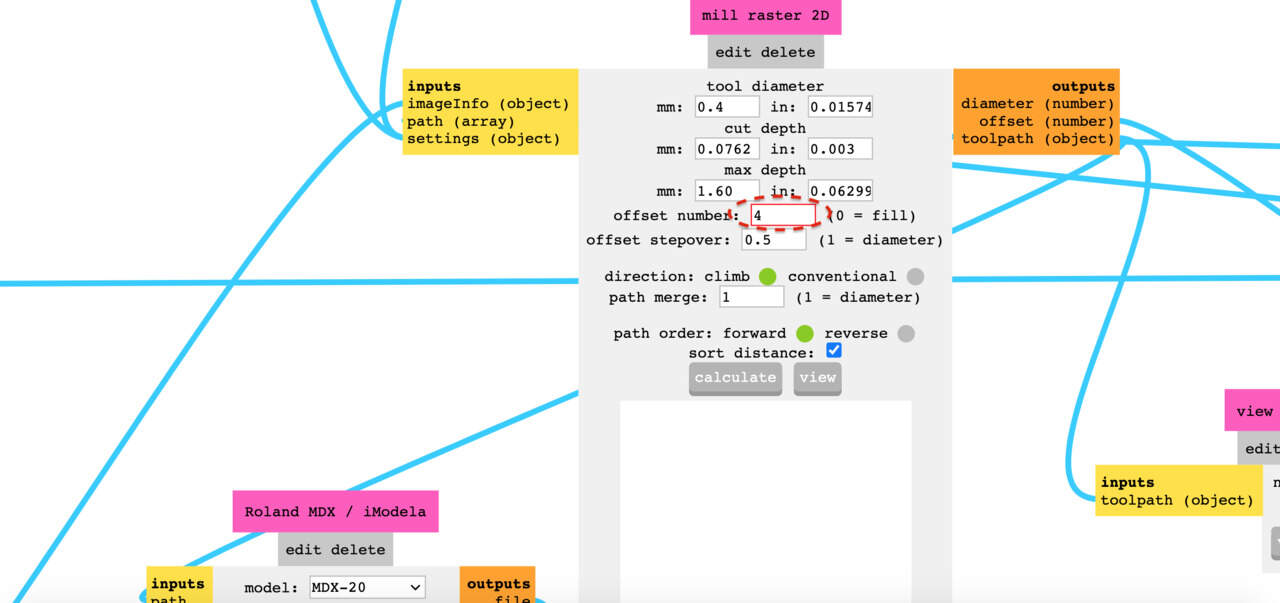
We go to the mill raster 2D and enter the following parameters:
Specify the tool diameter, we will be using a 0,8mm flute endmill.
Specify max depth: 1.60mm
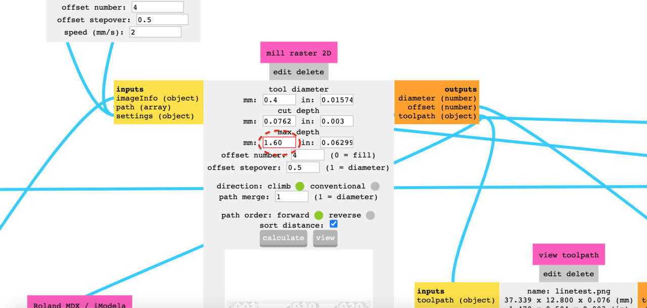
Specify offset to 1:
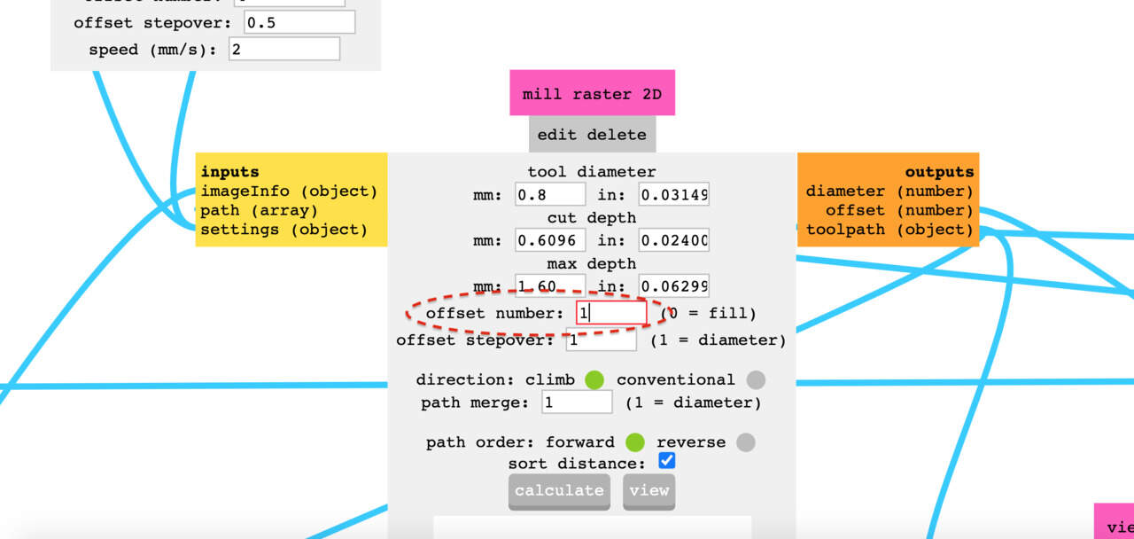
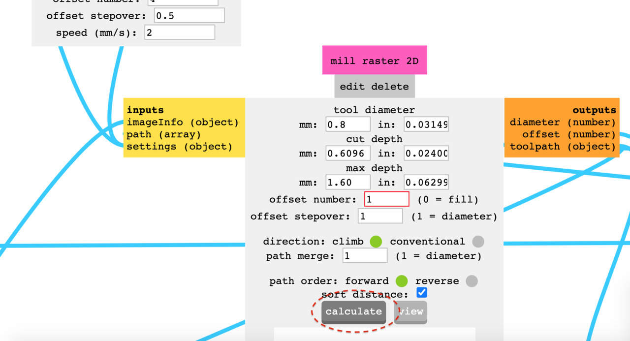
Press calculate:
Press view to be sure there are 3 lines:
-
Machine is already on.
-
Change mill and put a 0,8mill (for interior) with the same steps as before.
-
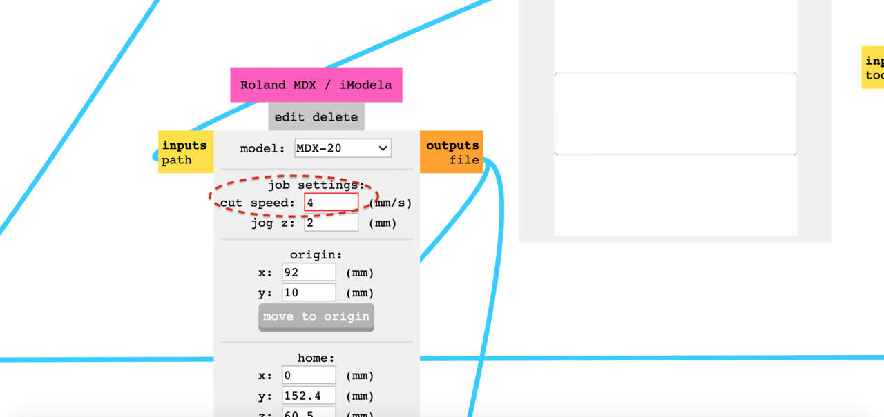
Go back to mods and change cut speed to 4:
-
Press move to origin to check where the origin in the machine is placed.
-
The origin is the same as before, check photo if necessary.
-
Go to machine and change z acis manually with the alan key just so it touches the board.
-
Cover machine with glass.
-
Go to mods and press calculate in mill raster 2D again (always do this before sending file):
-
Press send file so that machine starts milling:
-
When finished we vacuum the material left.
-
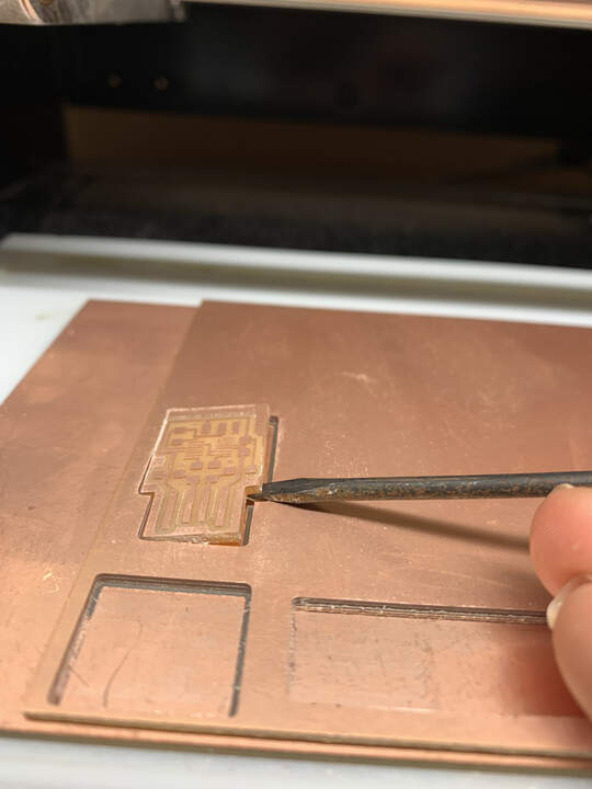
Take it out with screw driver
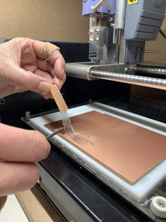
-
Sand it with paper
-
Wash top part with soap and water:
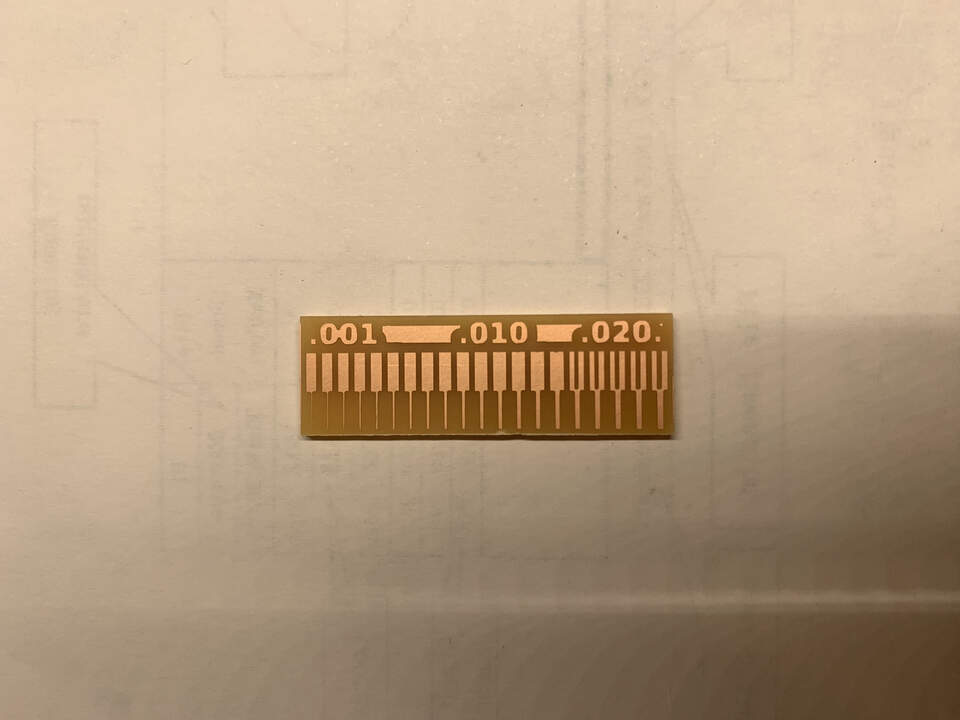
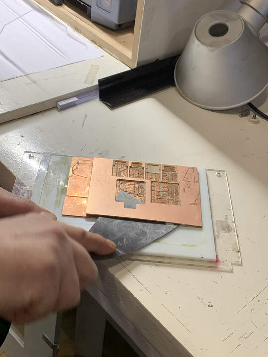
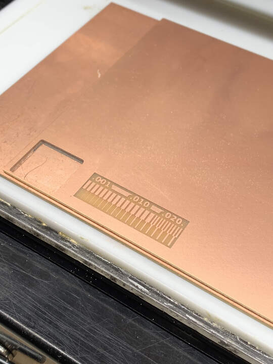
With this development what we want to see is how thin the copper lines can be and how thing they can go in between. This design is in inches, conversions below:
 0.020 inches is 0.4mm
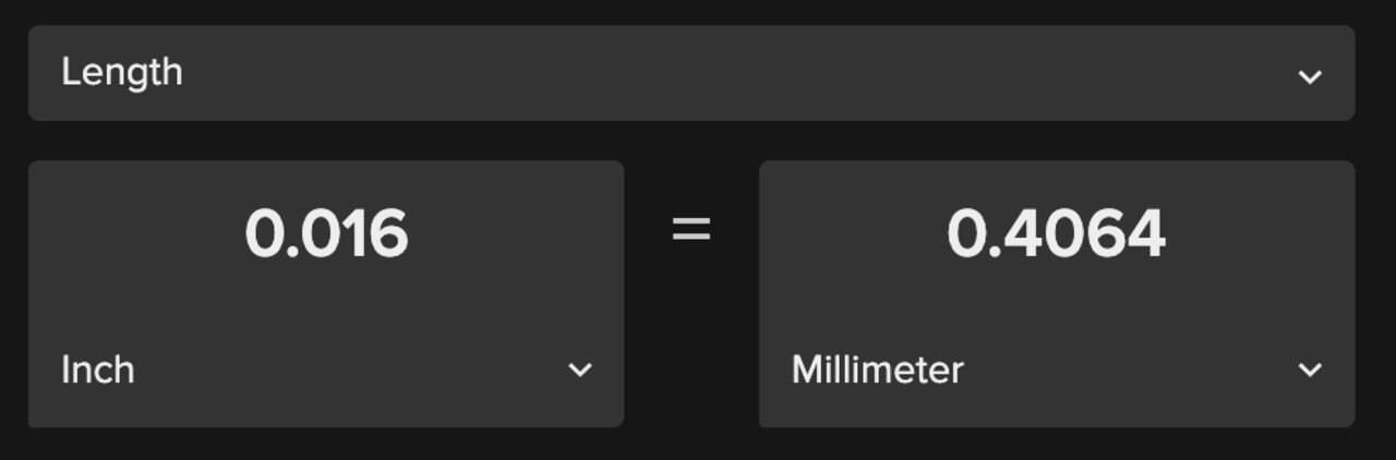 The width of the mill is 0.016 (it goes through in between).
The conclusion for this is that you can see how thin a line can be; thinnest line is 0.001 inches (0.025mm) and still looks good. This test also proves that the milling bit we were using is of 0.4mm, anything smaller than this will not be recognized in mods and will not be milled by the CNC machine.
The design of circuit boards will have the same milling process.
SOLDERING TUTORIAL
When we have the plates done, it is time for soldering. Henk did a tryout plate to show us how to assemble the components.
This is where we get all the components from at our Fablab, we will open draws one by one and when we take components out we put them back ourselves so material does not get mixed up!
You need to start with computer next to you with drawing where it shows which components will be needed and how they will be assembled
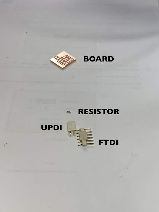
-
Resistor 1 4.99k you get it
-
FTDI header
-
UPDI header
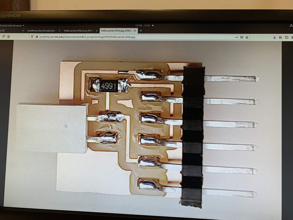
Assembled will look like this:
------enter ZEN MODE--------
-
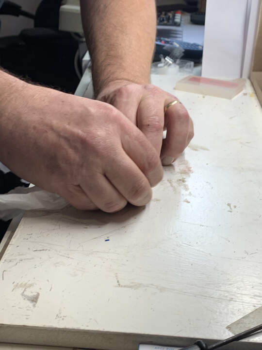
We will place each component with the tweezers.
-
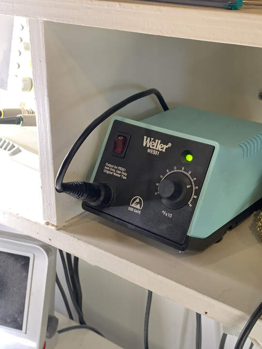
Turn on the solder iron. When the green light starts blinking it will be ready to use.
-
Turn on fume extractor
-
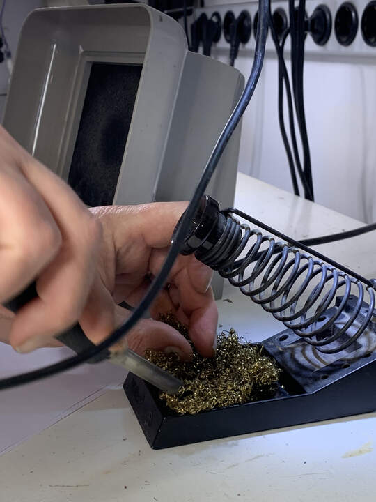
Clean tip of solder iron with sponge, a good way to clean it is to put some solder and clean again with sponge.
We will start from smallest component -> to biggest and from inside -> out
-
Put some solder, put the component in place -> solder the other side and do the other side better. When it is done -> remove the double tape from the back
-
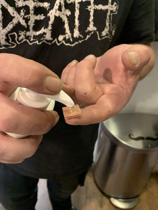
You can suck solder to eliminate excess or when making a mistake:
-
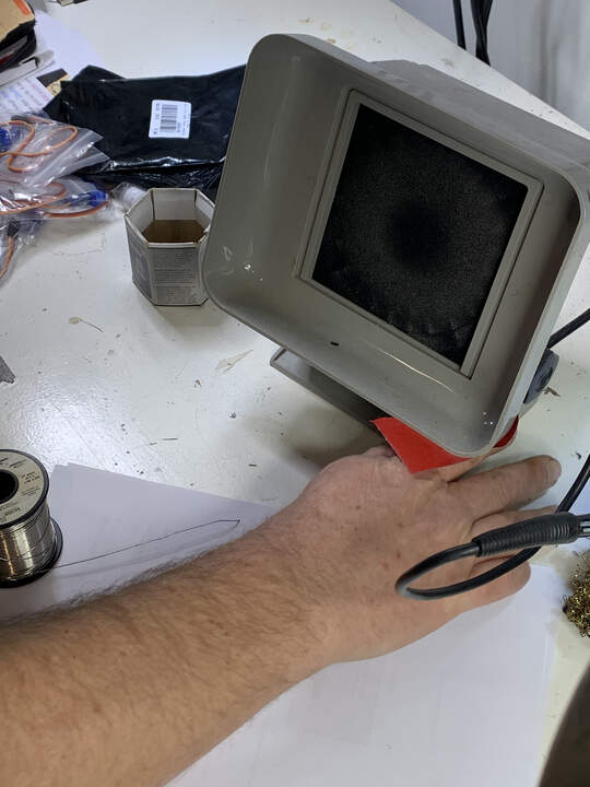
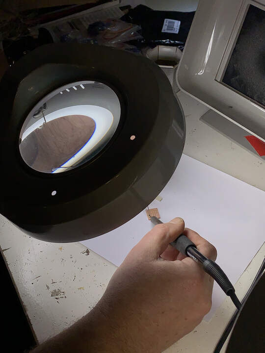
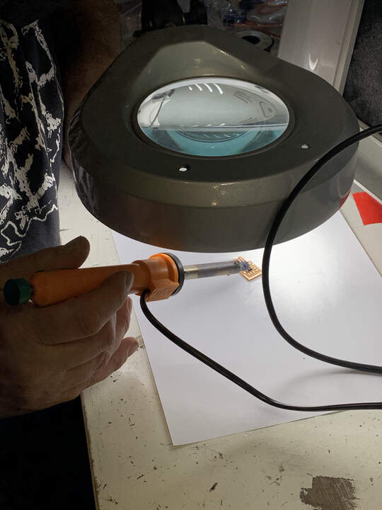
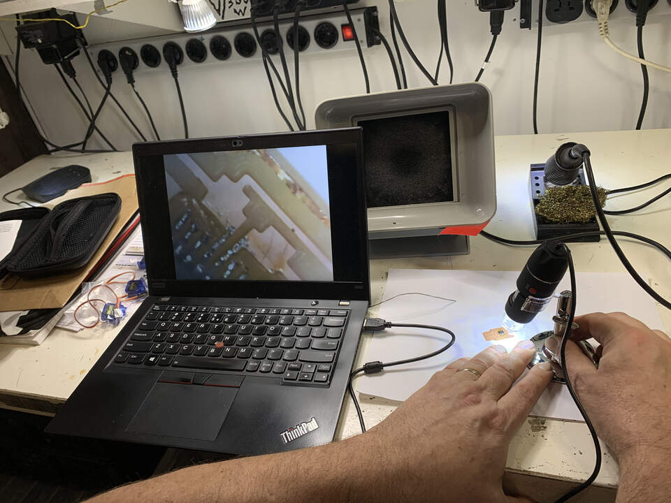
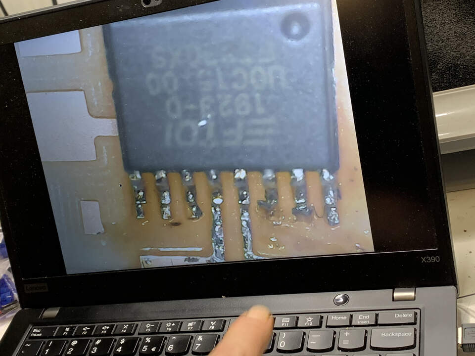
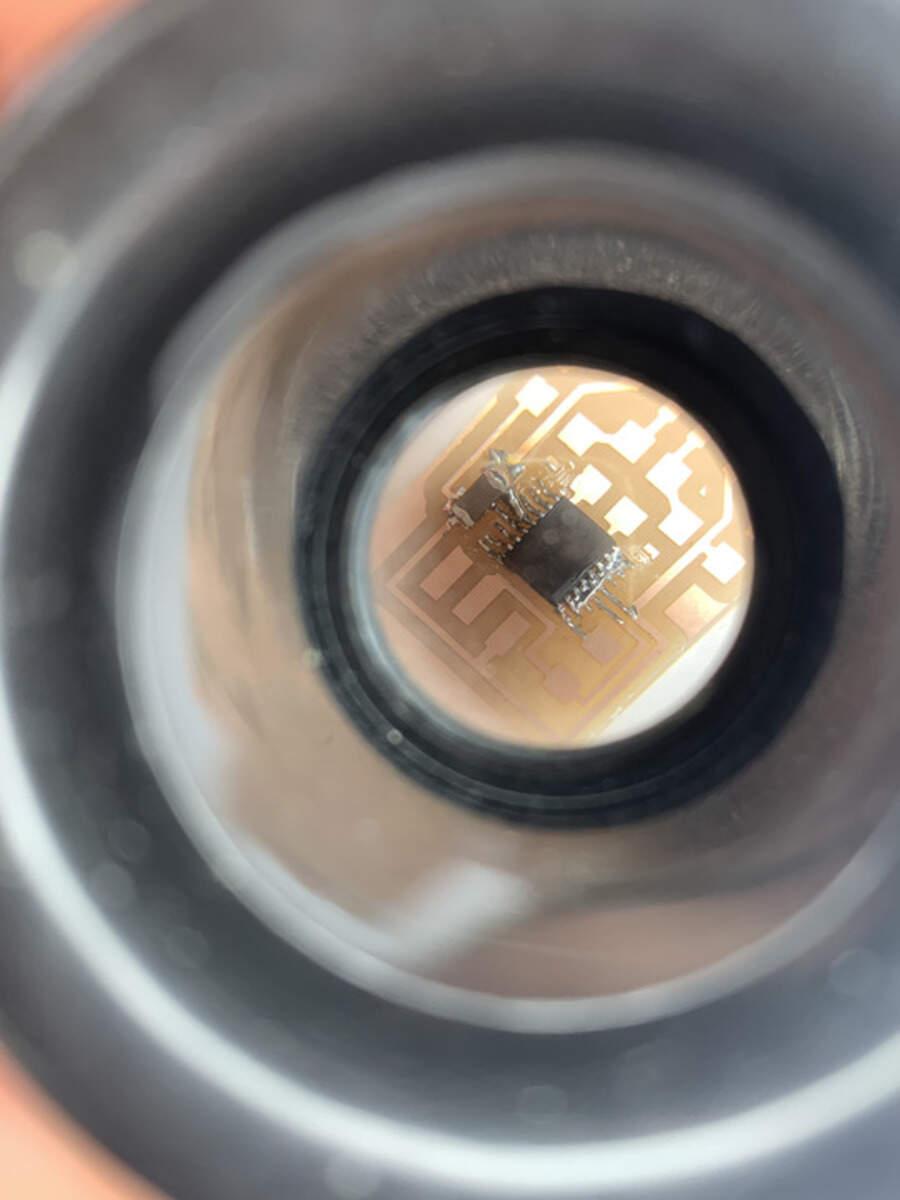
Check with microscopic camera if the solder is okay:
YOU LEARN THIS BY PRACTICE
INDIVIDUAL ASSIGNMENT: Make an in-circuit programmer by milling and stuffing the PCB, test it, then optionally try other PCB fabrication process.
There are three options to make:
-
Open: Mods project. Right click on top left menu > programs > open program > MDX mill > click on PCB
-
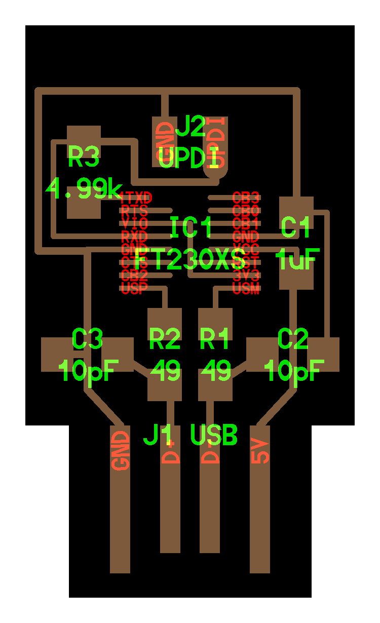
I will be doing the following circuit:
-
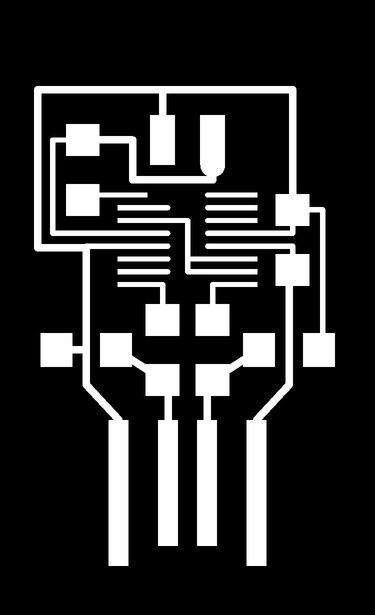
Insert png file:

-
I will follow the same steps as with the group assignment, the only difference will be the png files which I will upload to Mods.
-
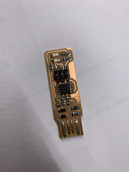
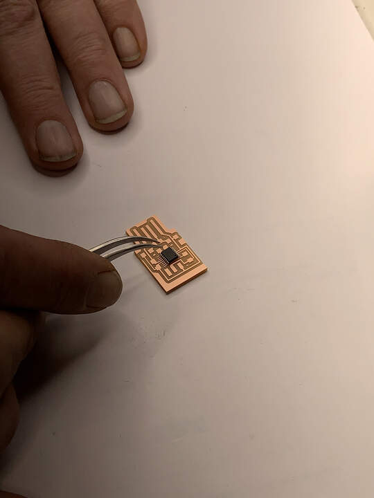
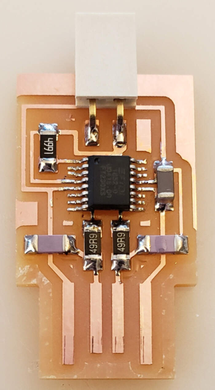
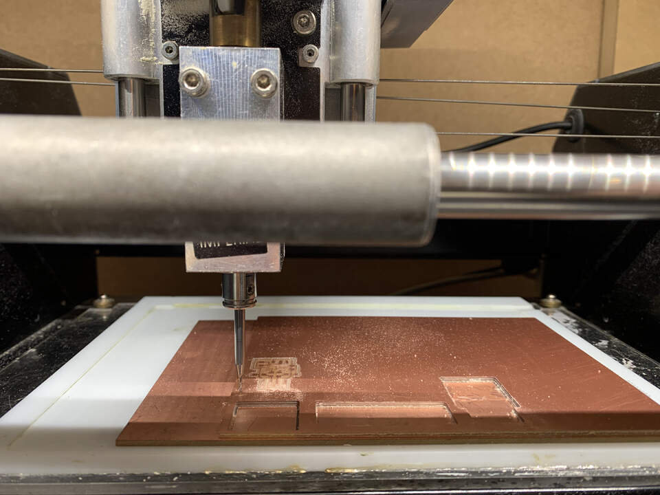
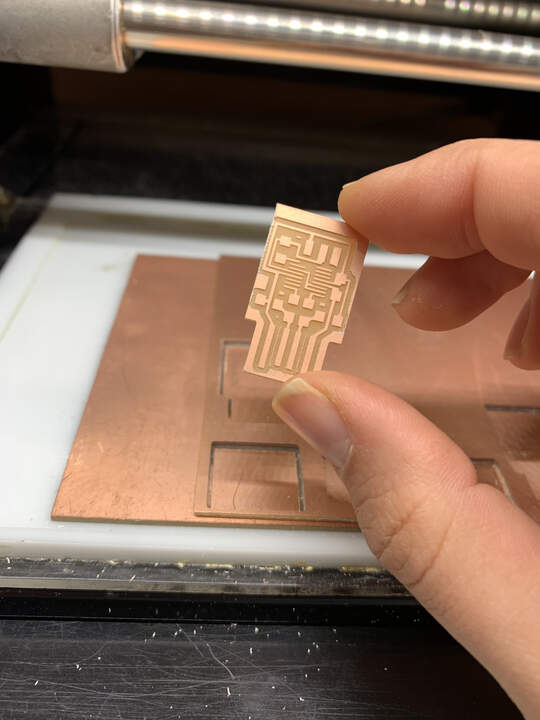
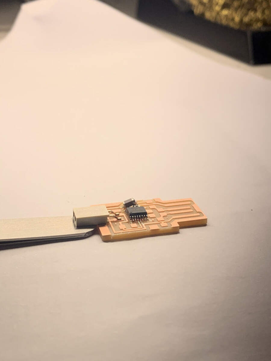
I milled option USB-FT230XS-UPDI:
-
My board looked like this:
-
After vacuuming:
-
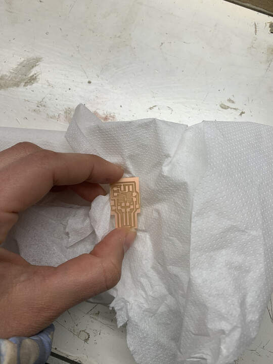
I took it out and sanded it with paper:
-
I washed it:
-
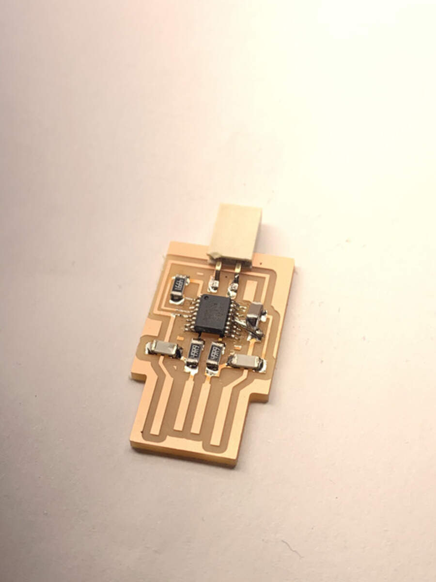
Soldering board: I will follow the following guidelines:
I also used this video to learn how to solder the different components.
-
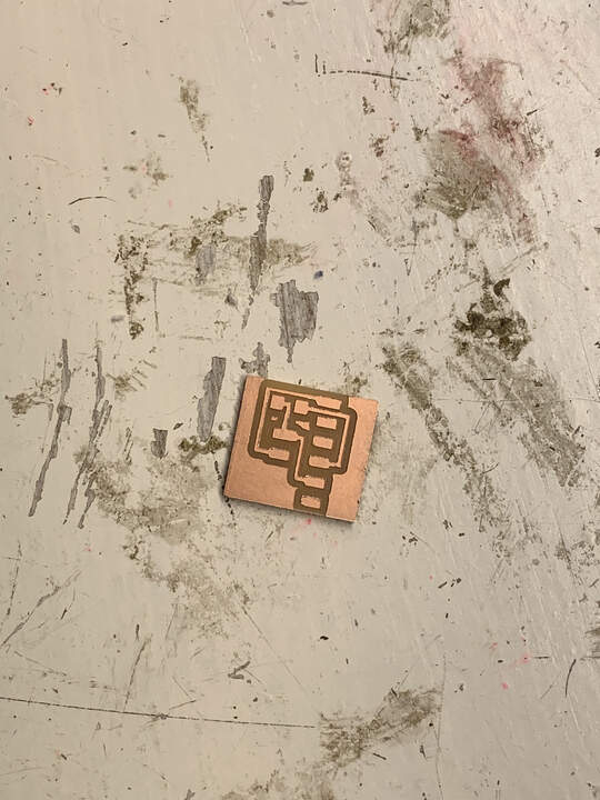
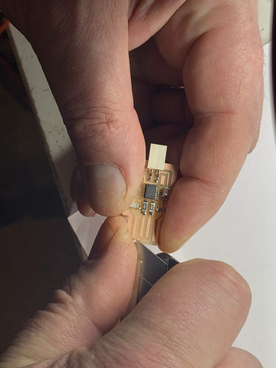
When learning how to solder the IC with Henk we messed up one of the sides so Henk showed me how to do a bypass (the copper trace had been destroyed) In this image you can see the bypass:
-
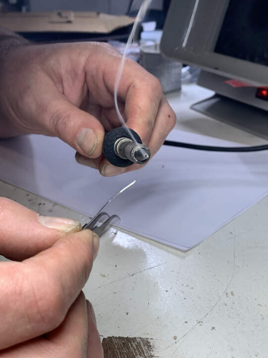
When soldering the UPDI, I used the tweezers as a trick in order to hold it in place straight.
-
This was how my circuit looked like in the end
-
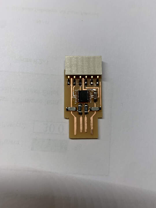
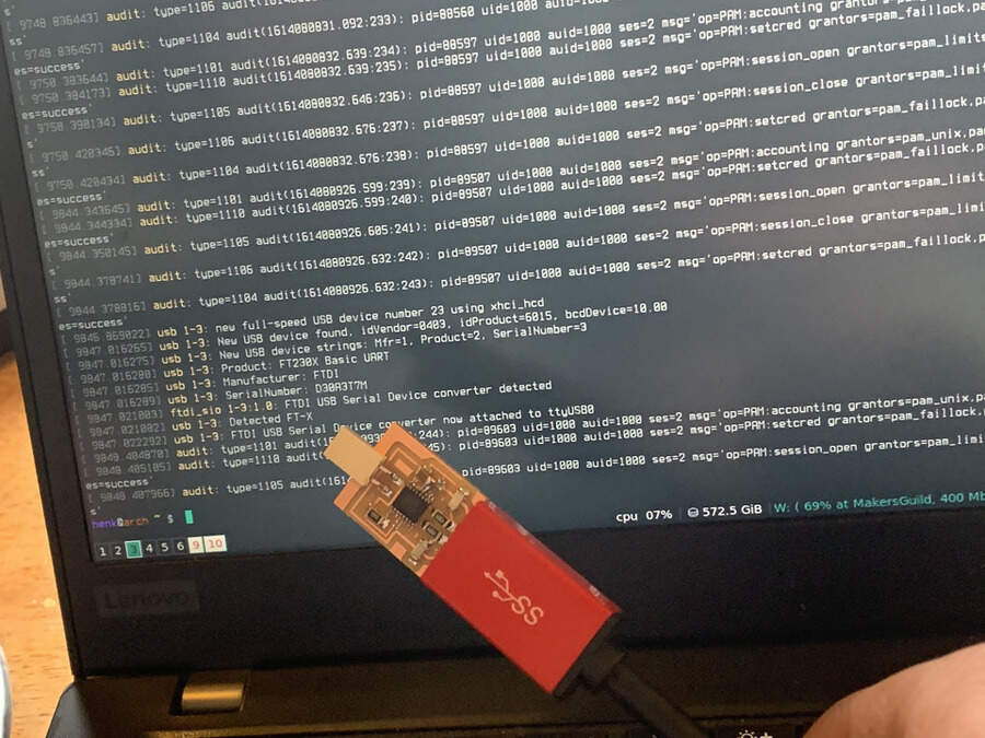
I had to remove this piece of copper in order to avoid getting a short when connecting it to the computer.
-
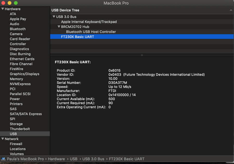
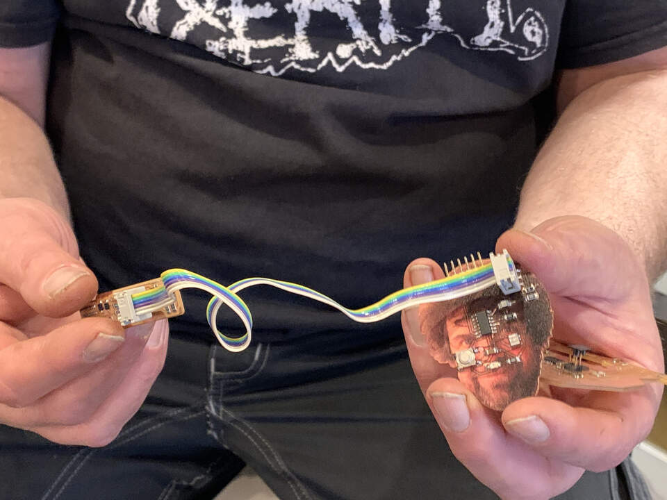
I connected it to the computer and wala! works!
-
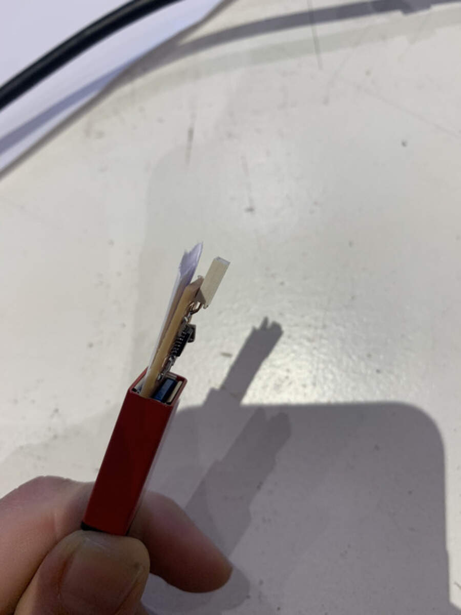
We had to use a piece of paper in order to make it work properly on my Mac.
-
This was the result of connecting it to my computer. To check if it is was working I had to go to Apple > About this Mac > System report > USB