7. Electronics design
For this week, we have to
- redraw the echo hello-world board.
- add (at least) a button and LED (with current-limiting resistor)
- check the design rules, make it, and test it
- extra credit: simulate its operation
Introduction
I’m an architect designer… Still learning what is the basics of electronics… So the assignment needs weren’t clear to me at first.
So with my first board design here, I did a lot of things that made no sense at all in the electronics!!
For this assignment, we need to blink a LED and control it with a push button, that will be happened when we program the microcontroller ‘attiny44’ with a code ‘Arduino, C … else’ to control in the LED and the button.
Before this step, We need to program the microcontroller ‘Attiny44’ with the programmer that we made in the electronics production week.
I realized this Introduction after I have been fault in the first design that I will explain, and reach to the point that I don’t know how I will continue!
So I reback to a reference for me Mrehan Elshehawy ‘Fab Academy 2018’, and reviewed her assignment for this week. I noticed that, she used the microcontroller ‘attiny44’, FTDI, ISP headers, LED and button. Just this Components.
For my case, I added USB component to this board with no reason why I made that!!
So I reviewed another assignments for different students, all of them used the same way. Then I asked my instructor Kamel, he explained me this Introduction… So, now I understand what I will make.
We can start again!
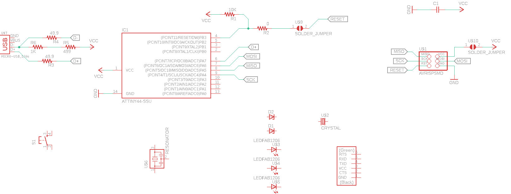
Redraw the echo hello-world board
Fortunately, I have a previous experience with Eagle, So I used Eagle for this week again. If you like to review the DRC, Process of how we can use it. Please cheack Electronics production week, this is a perfect recommendation from Ohad Meyuhas ‘Our Guru’, that it will be perfect to learn eagle software from two weeks, and make our own design for USBISP. So I saved my time this week to learn more about the electronics design not technical learn with software.
Actually, I so excited to use KiCad this week, but I chose to finish my assignment first, and if I have more time we can try new software.
- I added the Fab library in week05, So we just add it one time.
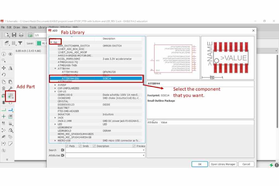
- I add part as shown in the last image, then select the fab library and added all my components that I need as shown in the next picture.
- Attiny44-SSU.
- FTDI-SMD-HEADER.
- AVRISPSMD OR PINHD-2X3-SMD.
- RESONATOR.
- 6MM_SWITCH6MM_SWITCH.
- CAP-UNPOLARIZEDFAB.
- LEDFAB1206.
- RES-US1206FAB.
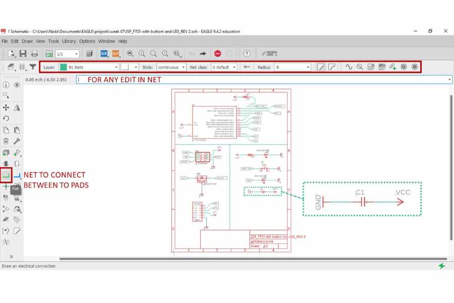
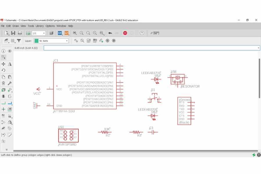 Then I used net to connect between 2 pads.
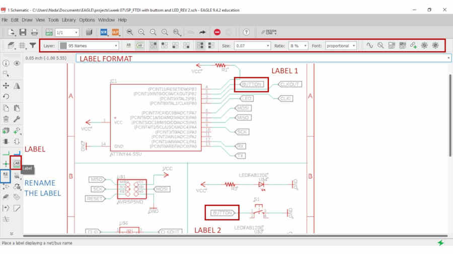
 From the label button we can connect between 2 pads in the same schematic, We just rename the two labels with the same name. Also we can rename the label as shown in the picture.
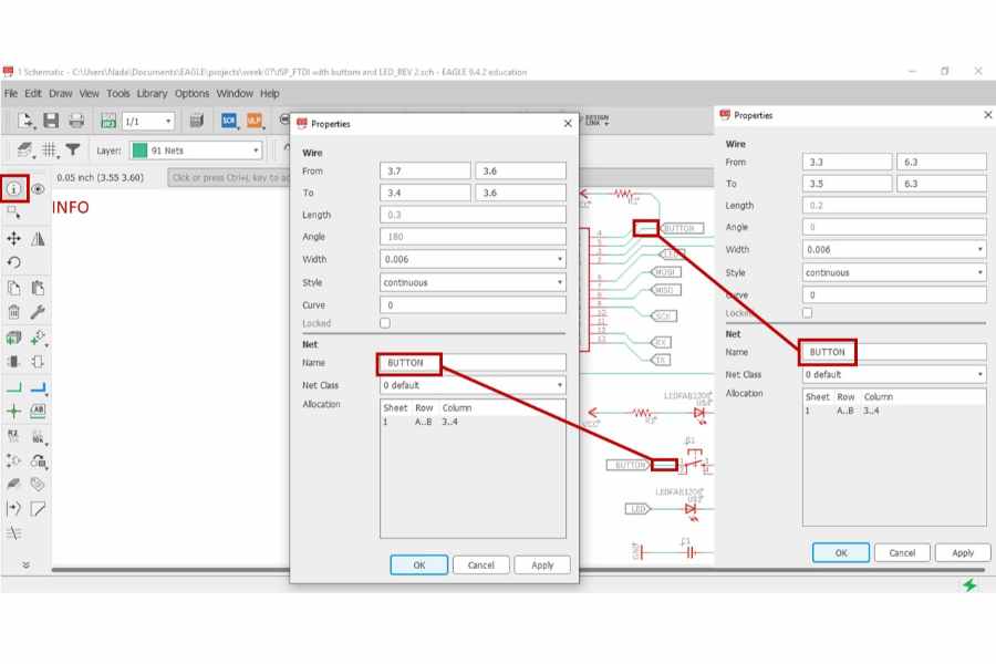
 Make a small check to make sure the net is connected with the right pads, press Info, then select the required net as shown. It should have the same name with the second pad.
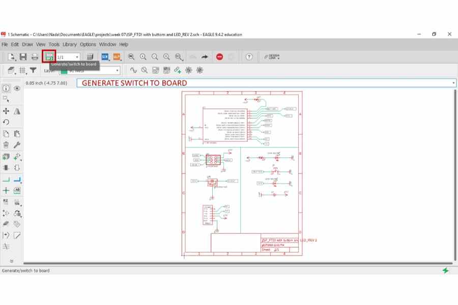
Now our schematic is completely ready, we have to generate this schematic to layout as shown.
 We will have this preview!
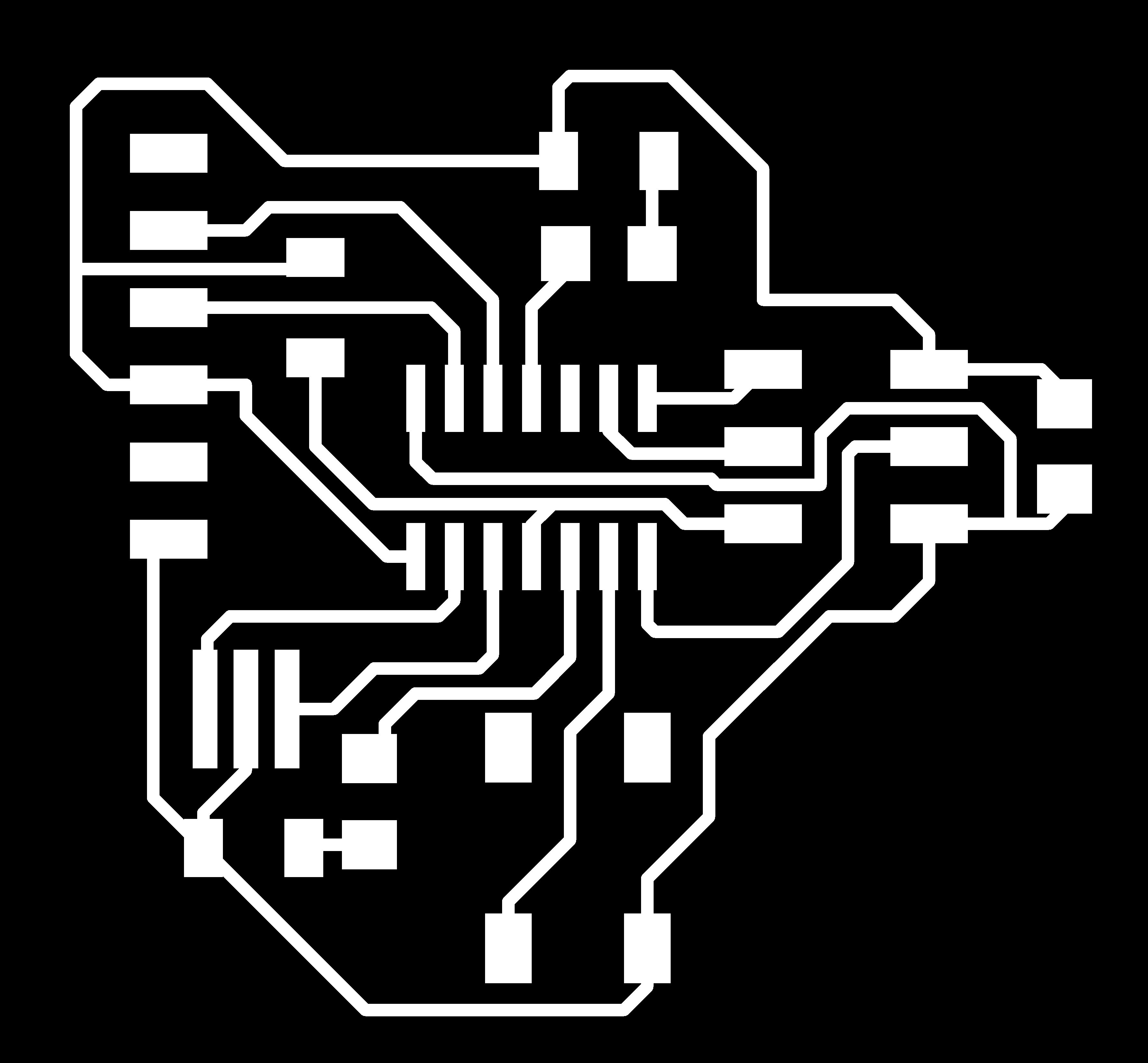
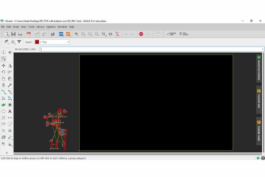 So we can move any component to the right place we want and start to route the traces.
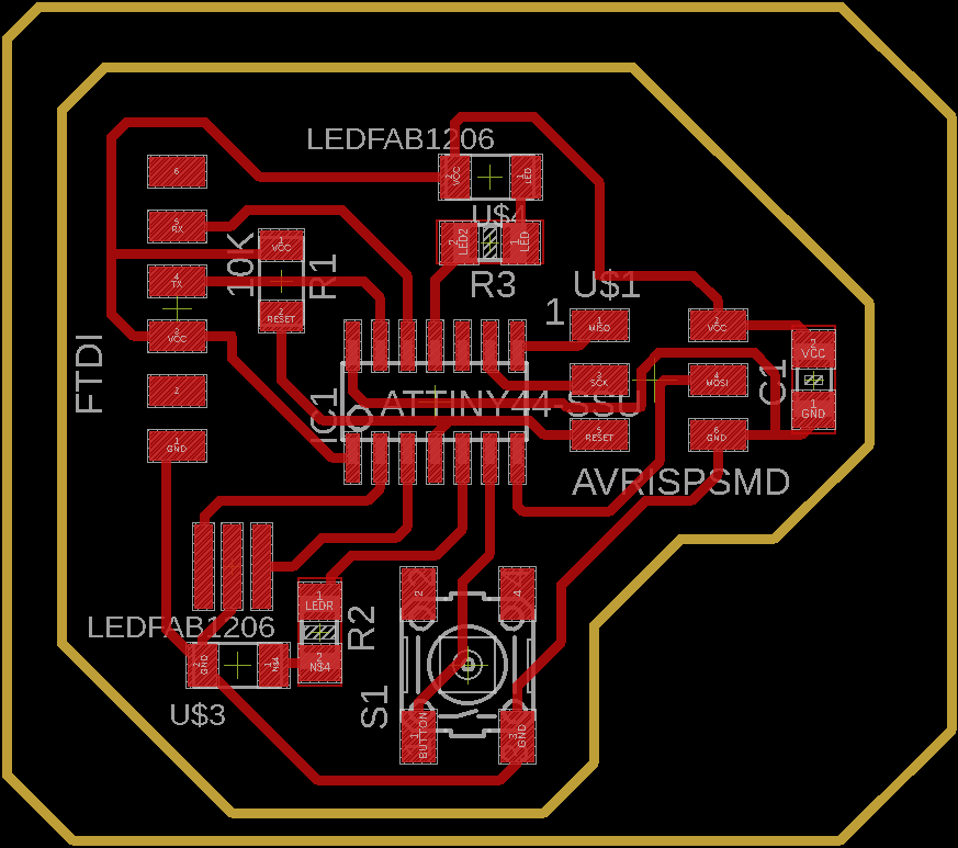
 Finally, I reached to this result!
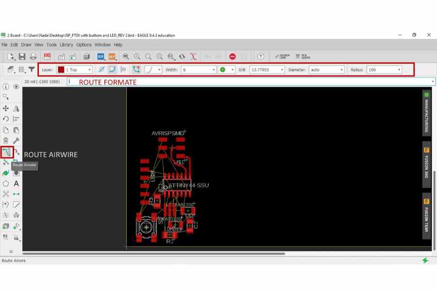
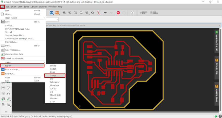
Export Images From Eagle
For this step
- We need to hide all layers that we don’t need, as we made in Electronics production week, also the pads and traces names to make export as PNG.
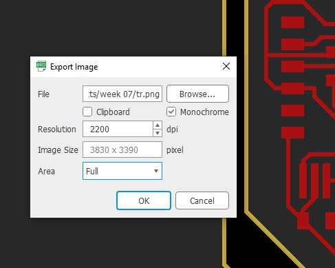 I chose monochrome to export image with black and white. Also increase the dpi to 2200. Then ok…
Then close the traces layer and make the previous step.
I chose monochrome to export image with black and white. Also increase the dpi to 2200. Then ok…
Then close the traces layer and make the previous step.
So this the result!

Edit Images with photo editor
Then we need photo editor to make edits as we explain in Electronics production week.
So, I usually use photoshop in any photo edit, but I want to learn a new tool, So I decided to used GIMP during this diploma!
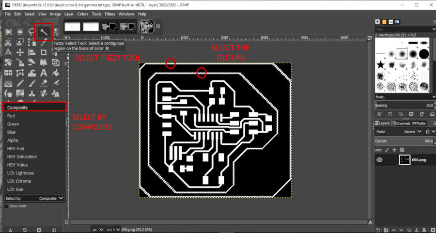
- opened the image with GIMP.
- Select fuzzy tool to select one color and make sure you selected by composite.
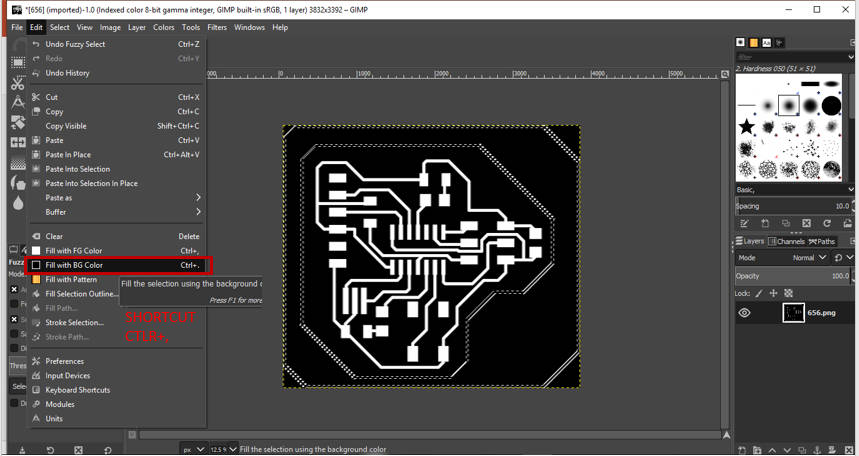
- Pick on the outline that we need to replace the color to black, use ‘ctlr+,’ .
- Now you have the traces image ready to mill!
We will repeat the previous process to the outline image to change the color.

We now ready to use Fab Modules to generate the code to the machine.
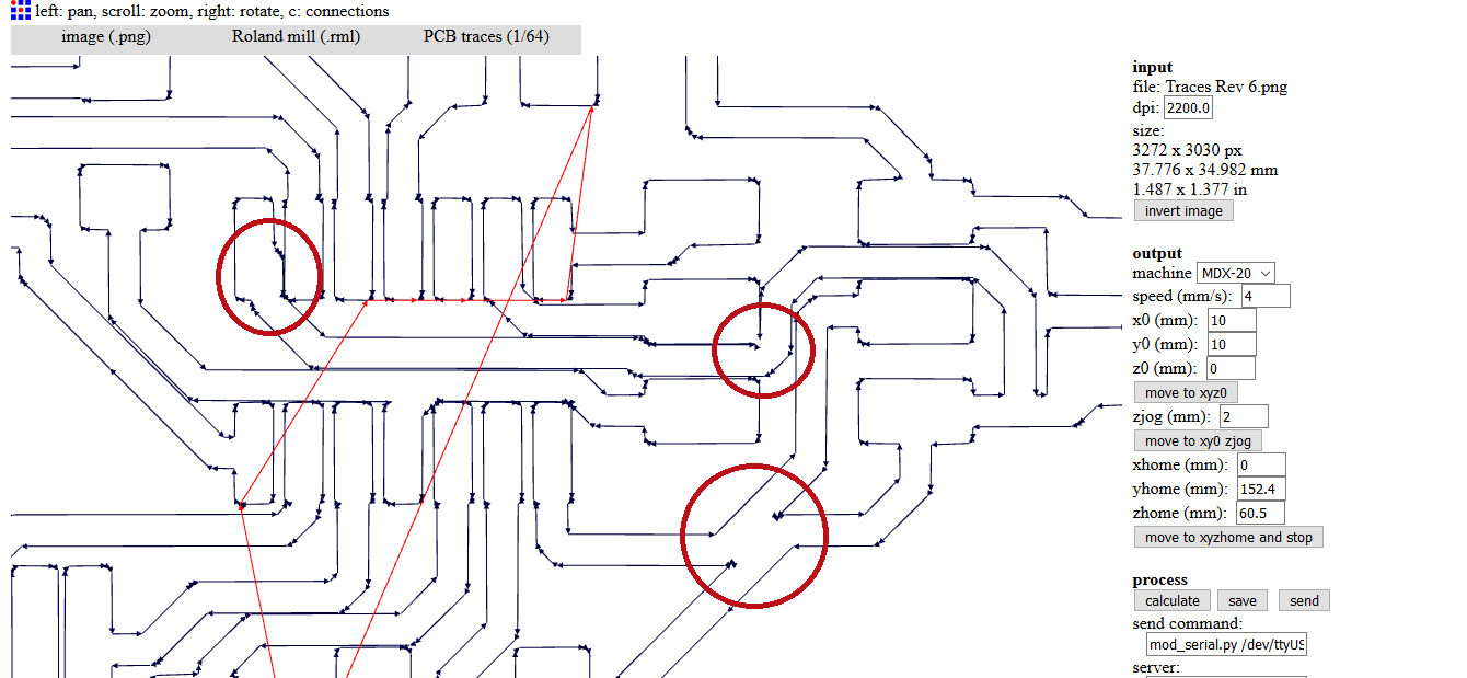
When I calculate the traces I noticed that, there are some traces wouldn’t be mill. So the solution for this point is reback to eagle and export the image again with dpi 2400. Then repeat this all process again!!
Fab Modules
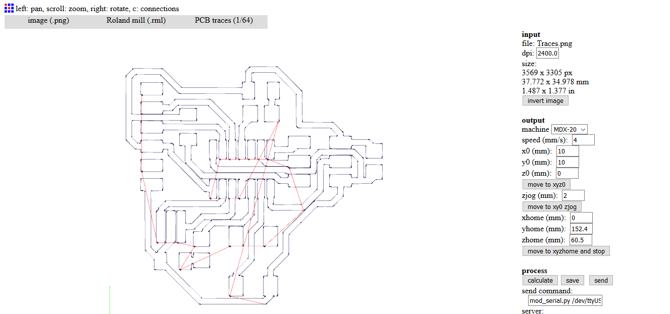
So after repeat all previous process with 2400 dpi, Our PCB is ready now to mill.
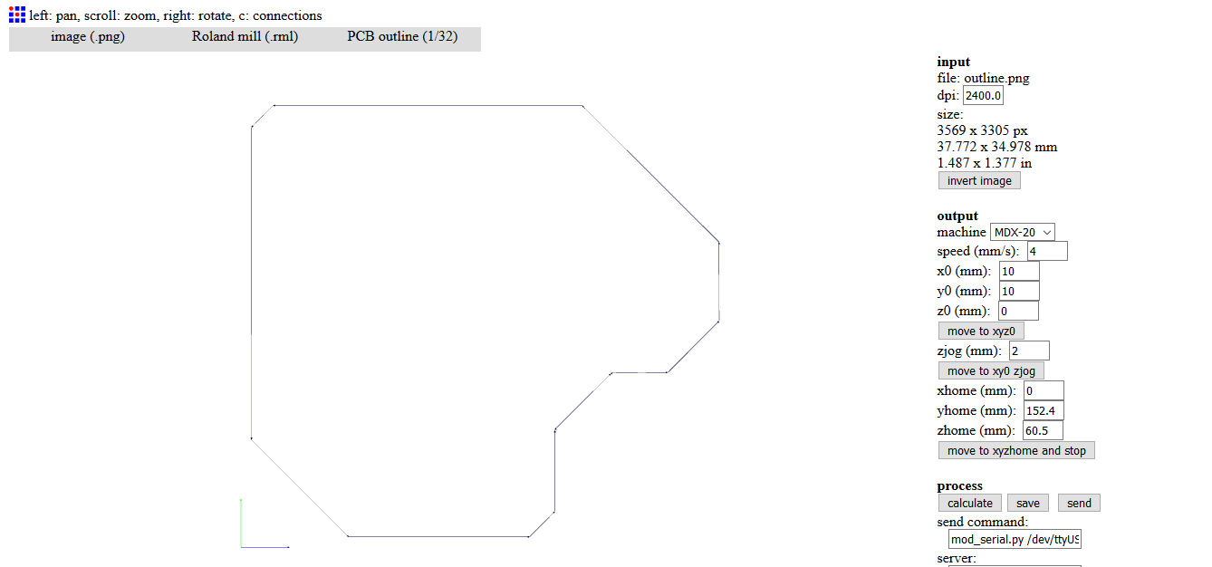
Fabricate The Board
I followed all the steps that I have been made with the machine inthe electronics production week.
- Fix the PCB with double face tape.
- Put the endmill 1/64 for the first process ‘milling traces’.
- Edit all setting in fab modules, calculate, then send the code.
- For the second process, Change the endmill to 1/32.
- Upload the outline image, and edit all setting in fab modules.
- Start cutting!
Happy watching!
Milling Blink LED with Button PCB from Nada Gamal on Vimeo.
In this video, during the milling process… I noticed that the PCB was moving in the Z direction… That’s mean I didn’t fix the PCB well… That will make errors … and I should be very carful till I finish this PCB, especially in the cut process.
This is the final result for the first process
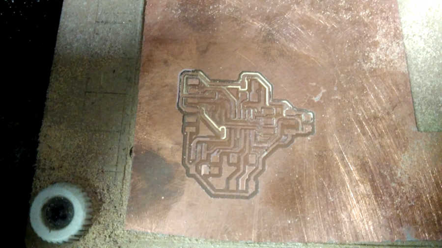
So, It’s very clear, that there are a lot of errors with the milling process cause of the Z direction. But the all traces are milled. So we can continue and take care in the next time.
Unfortunately, I didn’t have pictures for welding process. I forgot to take pictures! This point is also what I learned from this assignment, we have to take pictures of every step we take to document them.
Programming
Now, we reached the end point in this assignment, and the same time is the risk point that can bring us back to the first point!!
This step will show us if our design and PCB is right or not!
Let’s see!
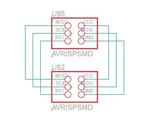
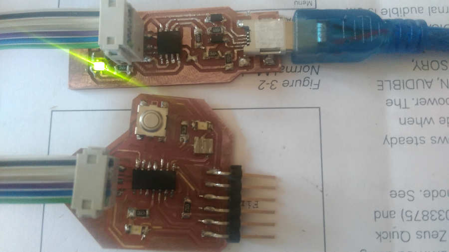
First I connect the ISP headers for the two PCB ‘USBISP and Hello echo world’ with the same pins as shown.
Then I followed the steps in the electronics production week, used the Make file‘frimware’ to program the microcontroller
Finally, It works!
This assignment continue in The Embedded Programming Assignment, See you!