Week 6 - Electronics Design
This week's tasks are:
- Redraw Hello echo board.
- Add at least a button and a led with current limiting resistor.
- Check the design rules.
- Make the board and test it.
- Use the test equipment to observe the operation of the microcontroller.
Step1: Getting introduced to some concepts
- What is library in electronics design?: Every component has it's own library that tells what is the symbol of this component and what is his actual dimensions.
- What is schematic in electronics design?: A representation on electrical circuit elements with symbols and how these elements are connected to each other.
- What is layout in electronics design?: A representation of the how electronics component will be laid out in the board.
I read the introduction to eagle tutorial and it shows more about schematic symbols and layout.
Step2: Redraw Hello Echo board
I designed the circuit using Eagle program from autodesk
- Download the components library
- Create new project
- Start making the schmeatic
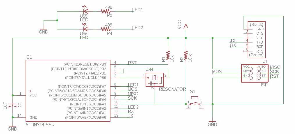
- ATTINY44-SSU
- CAP-US1206
- RES-US1206
- RESONATOR
- LED
- 6MM-SWITCH6MM-SWITCH
- AVRISP
- FTDI-SMD-HEADER
- VCC
- GND
- 1 mil=0.0254 mm
- 16 mil=0.4064 mm
- 12 mil=0.3048 mm
- Draw the board layout
- Generating the files required for fab modules
- Trying to add two leds
I downloaded the Fab Library From this link by right click on the link then save as and then I moved the file to C:\EAGLE 8.7.1\lbr.
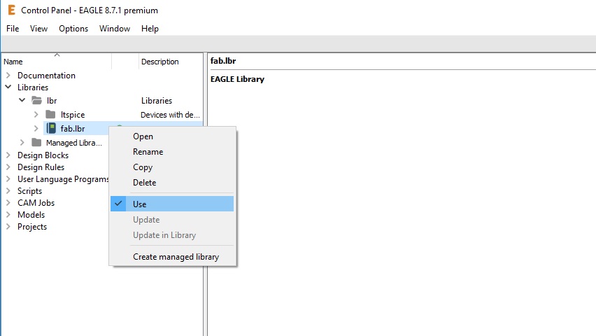
Open Egale program, Go to libraries on the left, click on the down arrow, right clik on fab library then select use
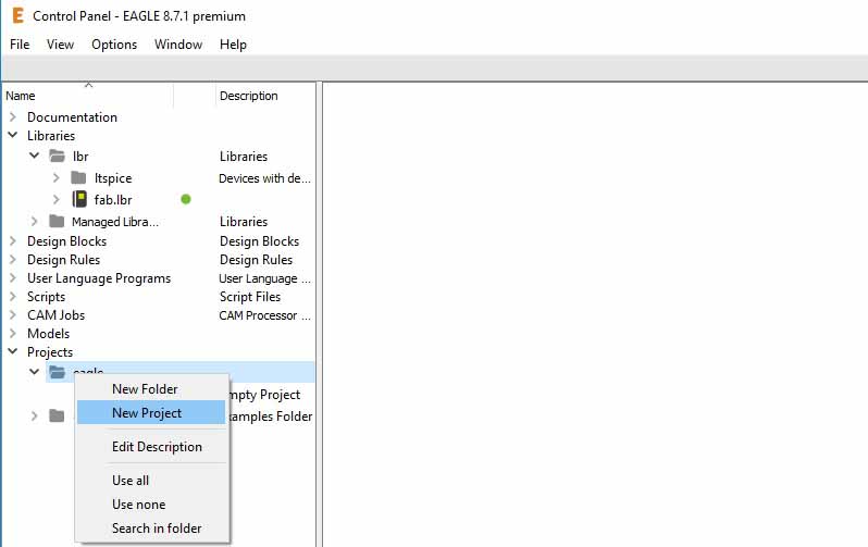
On the projects section on the left right click on projects and select "New Project"
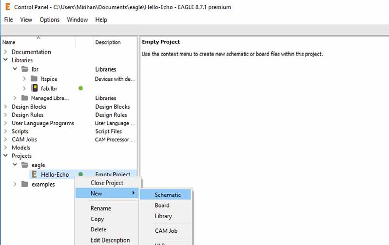
After creating a new project, Right click on the project name and select "New" then "Schematic"
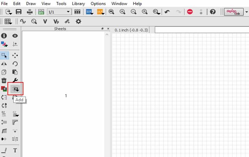
On the schematic page click on add tool to add the components we need
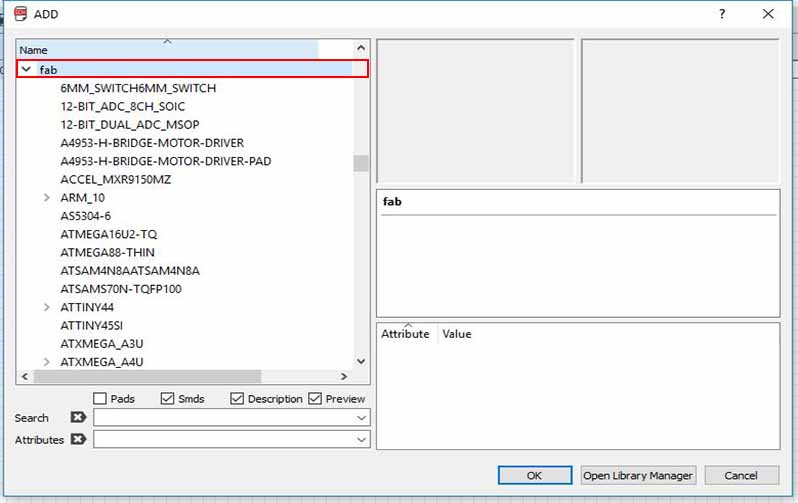
Adding the components will be through scrolling down in the fab library and choose the components.
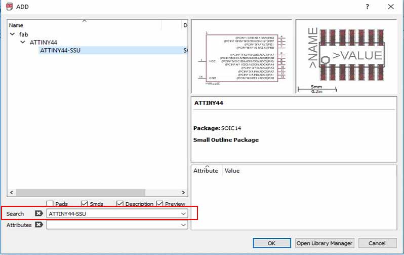
Or write the exact name of the component in the search area.
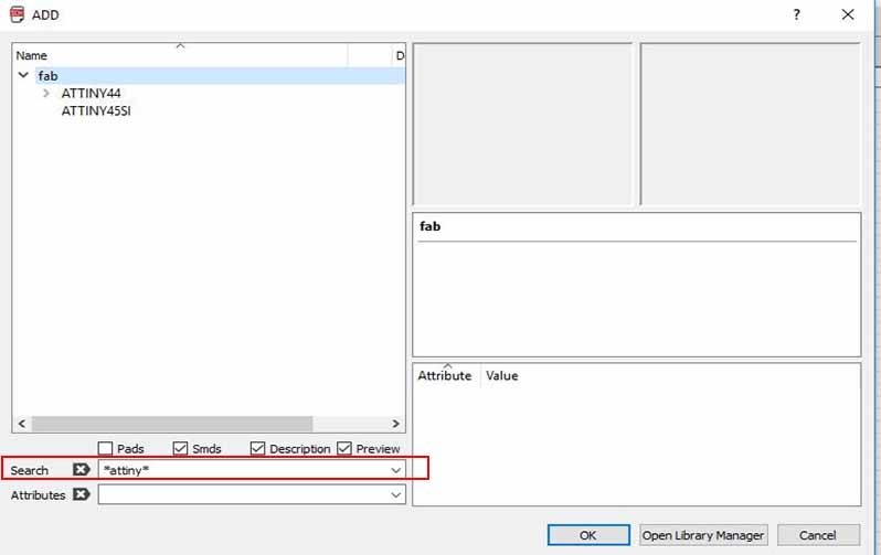
Or write the common name of the component between two asterisks ** then select the right one from the search results.
The components I added are :
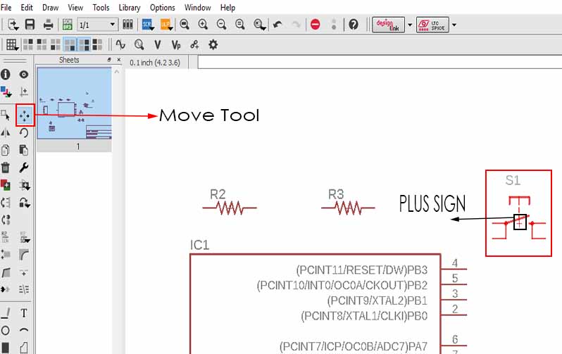
To move a component click on the move tool then click on the plus sign to activate the component then left click and drag and drop to the deired position. Rotation is by right click while the component is activated.
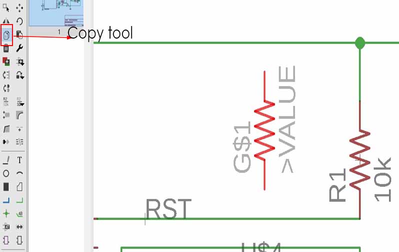
To copy component press on the copy tool then left click on the component to be copied.Another left click to drop it.
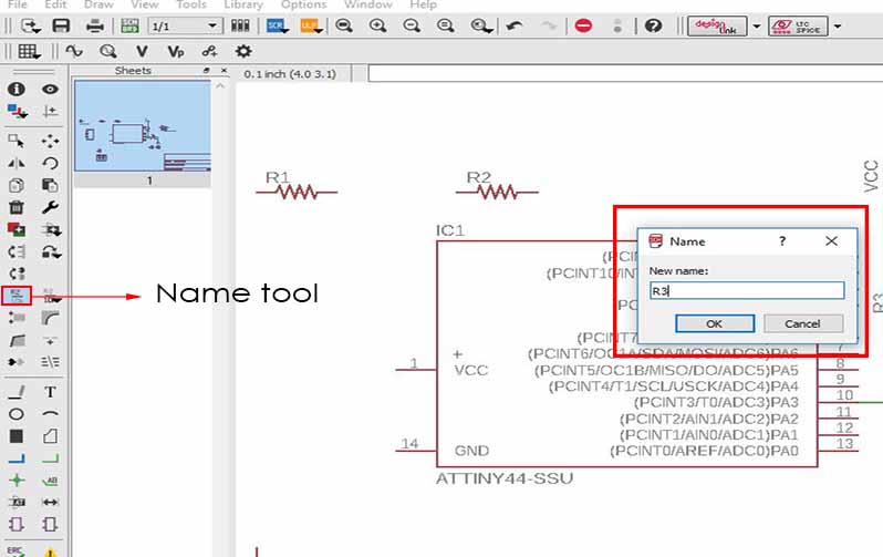
I renamed the resistors to be R1, R2, R3 by using the name tool.
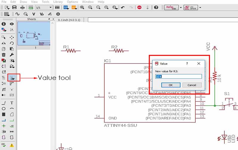
I changed the values of the resistors to be 10k, 10K, 499 by using the value tool.
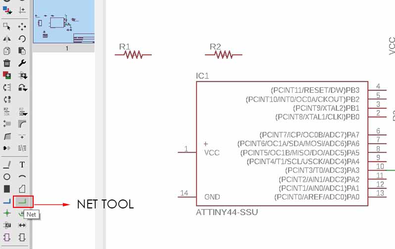
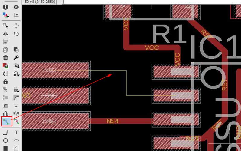
Use the net tool to connect between components.
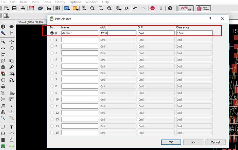
From edit I chose net classes to assign the minimum trace width and the required clearence between the traces. The clearence is assigned by the diameter of the milling bit
I will be using a 0.4 diamter milling bit which is equal to 16 mil so I set to 16mil and the traces to 12 mil.
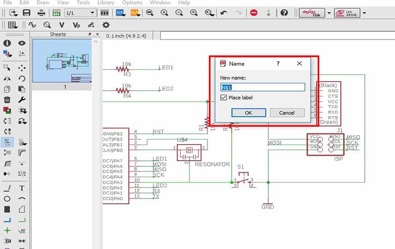
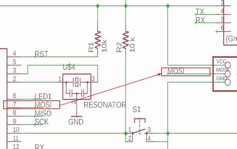
To avoid nets intersection, naming two nets with the same name will connect them to each other. I pressed on show label to show the name of the net.
By writing the sam name, these two nets are connected to each other
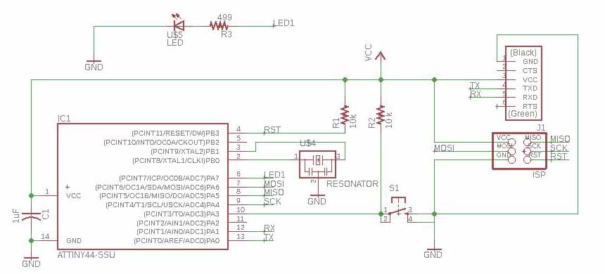
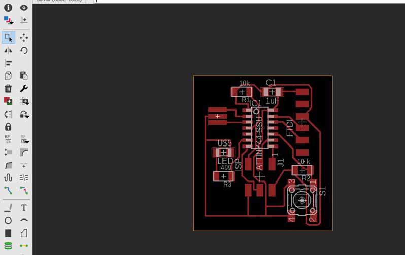
The final schematic
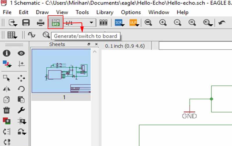
After finishing the schematic I clicked on generate board to switch to the layout.
I used the routing tool to make the wiring
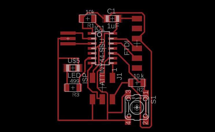
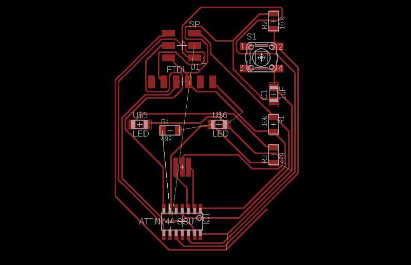
The final layout
Before generating any files we must make sure that the clearance between traces,the minimum trace width and minimum drill diameter (if exists) are right. If our milling bit is larger than these dimensions the Fab Modules will not see these dimensions and will not make paths for it. This will cause uncorrect PCB.
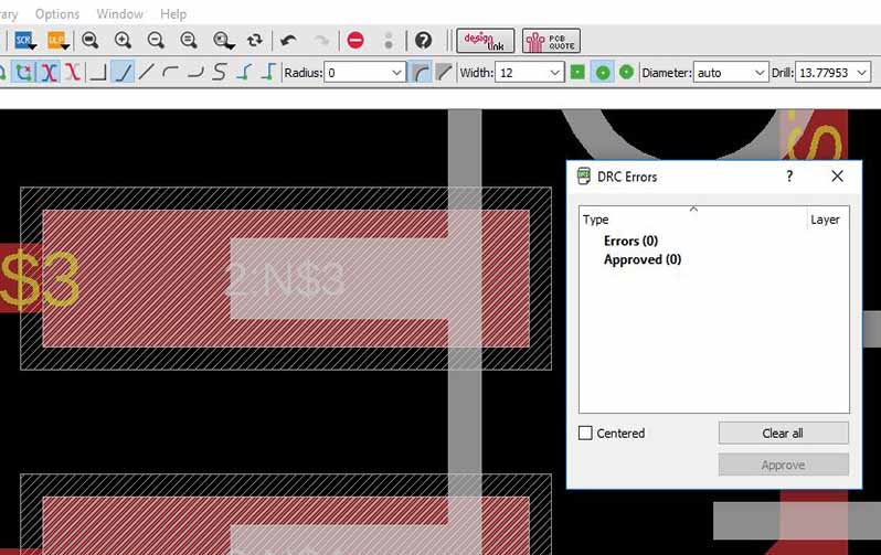
I opened tools, DRC, Clearance and set all values to 16 mil.
I clicked check and I got Zero errors. This means that all the minimum /clearance and dimensions in my board is correct.
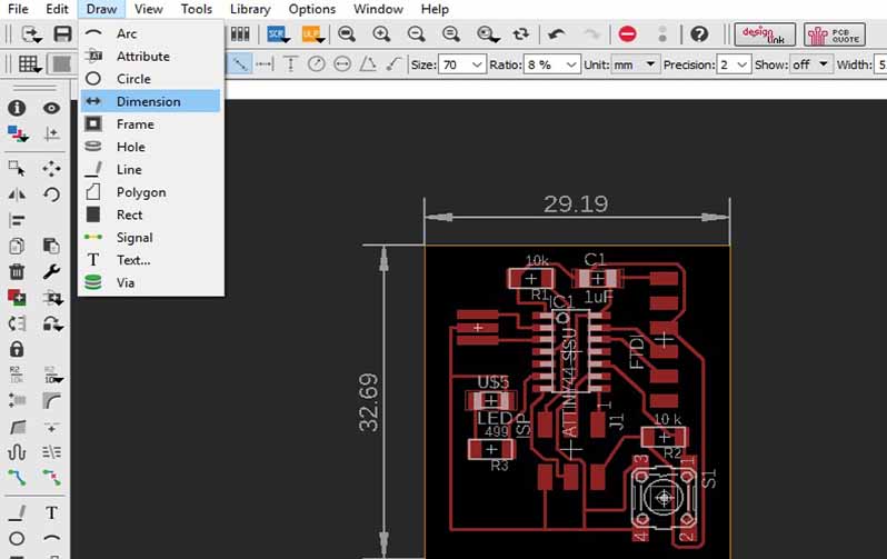
The frame should be resized to fit the board in exactly
I clicked draw then dimension and click on the height and width of the frame to make sure of my board dimensions.
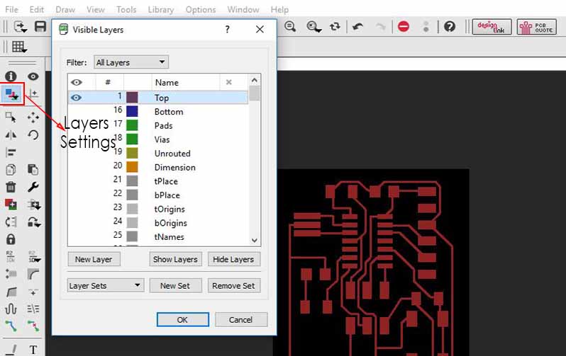
Once I made sure that the dimensions are okay, I clicked on the layer settings tool and hide all layers except the top.
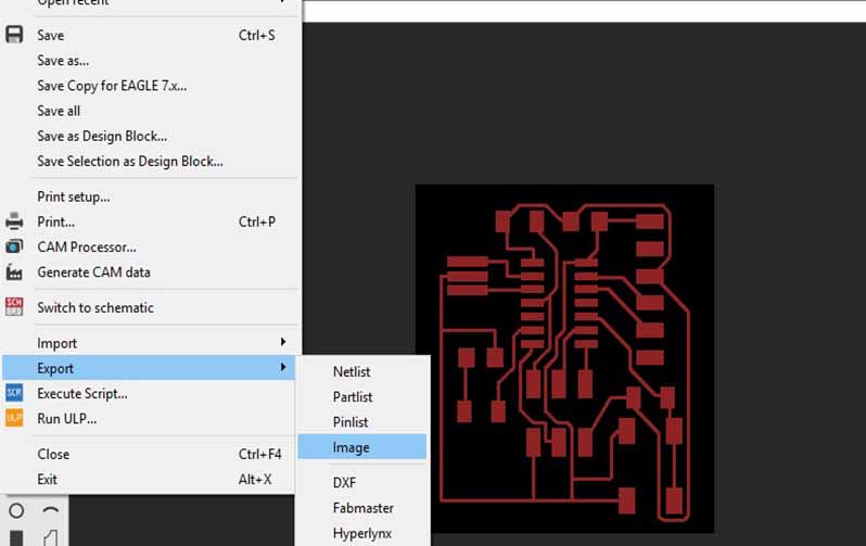
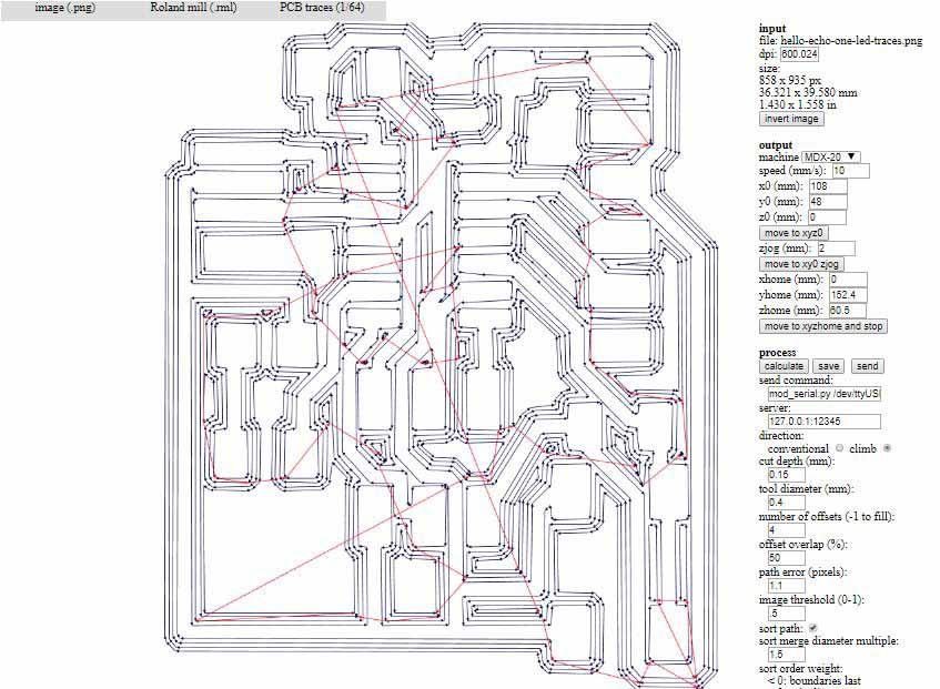
To save the traces image I clicked on file, Export then image.
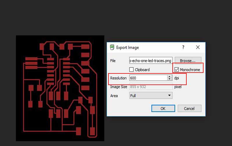
I chose the resolution to be 600 dpi and checked on monochrome to make it black and white.
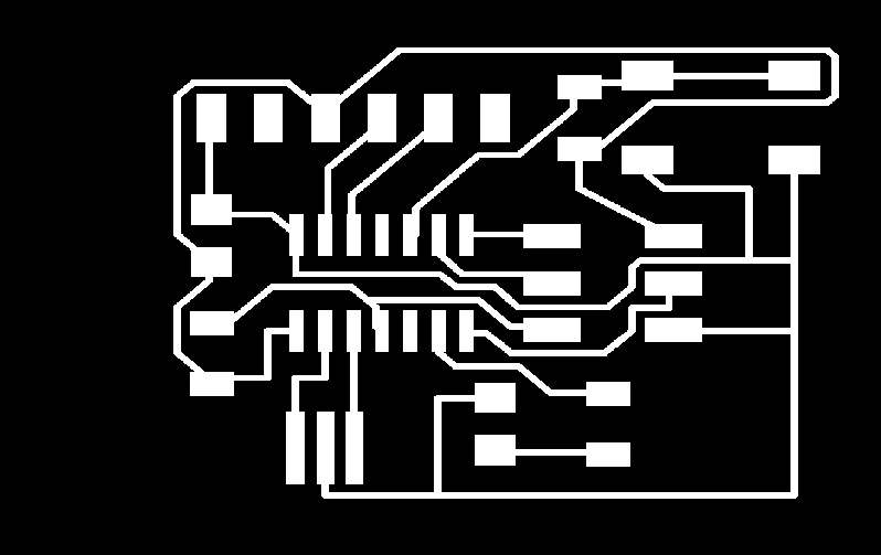
This is the result traces image and it's suitable for Fab Modules(traces in white and background in black).
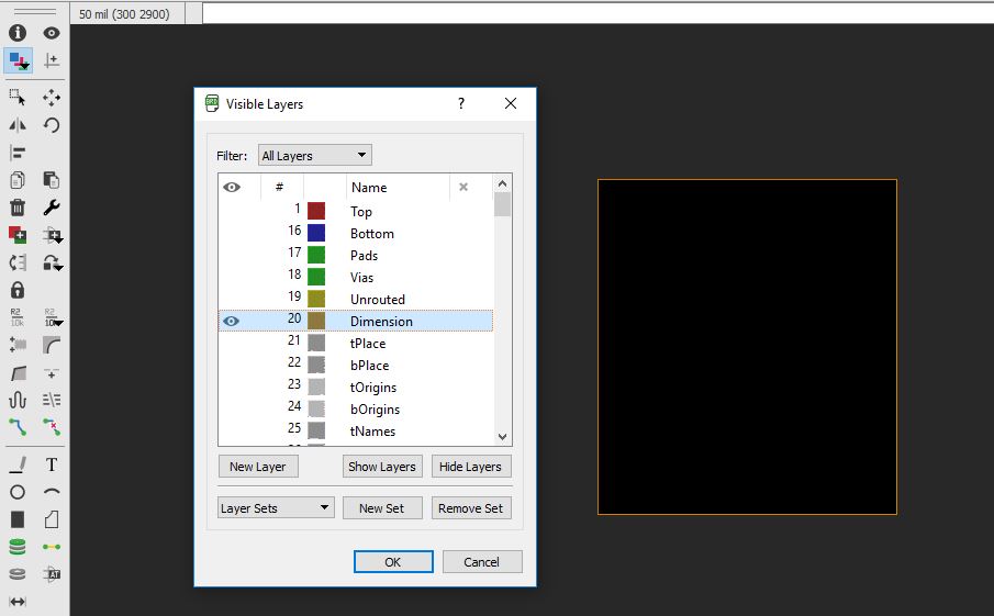

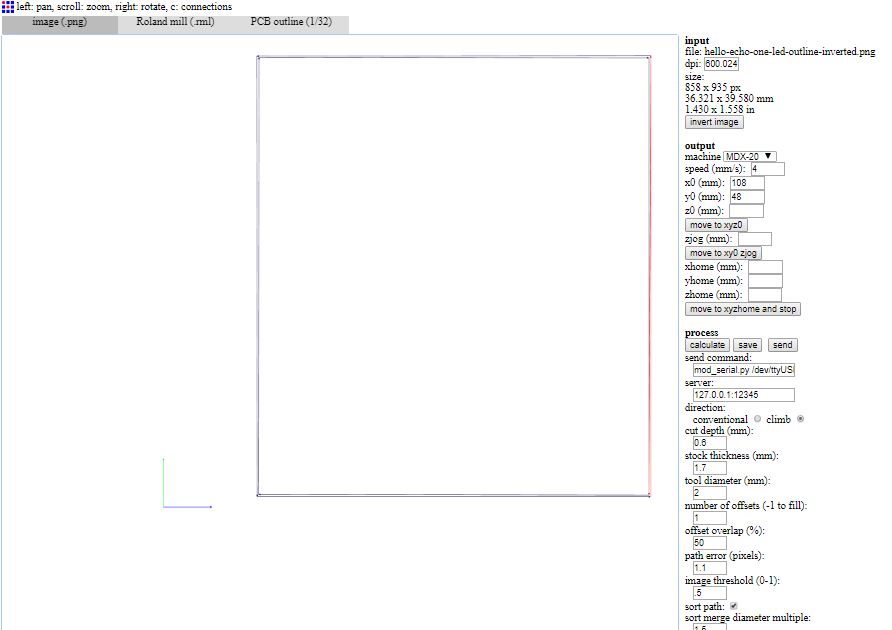
For exporting the border image I hide all the layers and showed the dimension only.
Export image with the same settings in this is the result of the outline image.The color should be inverted (border in black and background in white) to be suitable for cutting.
We need two images for each PCB to be millied one for traces ( traces white and background in black) and one for outline(outline in black and background in white). why? more details in Electronics production documentaion on get the needed files section.
I downloaded Gimp, It's an open source photo editing software that doesn't make any changes in photos size or resolution. Any change in the size or resolution is very critical as it will cause the two images to be un aligned.
From gimp I opened the image then chose image mode to be grey scale.
Then I chose color then invert and the traces become in black and background in white.
Now the images are ready for PCB milling.
I tried to add two leds and make the PCB looks like a robot face through the auto routing tool but it was hard to make it as a single layer and it seems that it should be double layer so I skiped it and went for milling the original one.
Hello Echo with two leds schematic
The robot face result
Step3: make the board
Open the traces file on fab modules and adjust settings for milling
milling on Roland modella MDX-20 using 0.4mm v-curve milling bit
I noticed that the leveling of the PCB sheet is not good and the machine is milling on the upper half only so I started the milling process again but added a small piece of paper under the bed on the lower half to adjust the leveling.
open the outline file on fab modules and adjust the settings for cutting
cutting on Roland modella MDX-20 using 2mm drilling bit
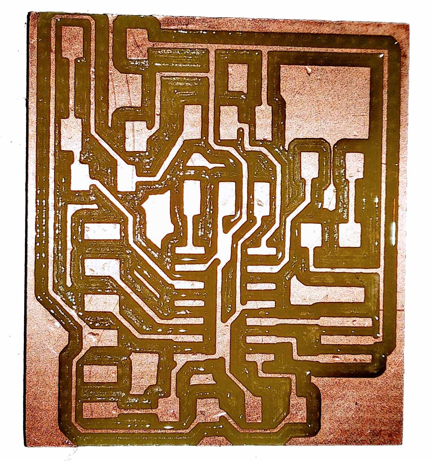
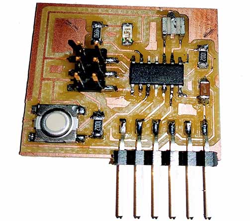
The final result
Step4: testing and soldering
I used a multimeter to test if there are any short circuit. This can be done by adjusting the multimeter to the buzzer function and connect one probe to line and the other probe to the other line. If the buzzer made sound, this means the two lines are connected to each other and there is a short circuit. If not, then there is no short circuit.
I started testing using this sequence
- Test the Attiny pins and make sure that no pin is connect to another.
- Test the FTDI pins and make sure that no pin is connected to another.
- Test The ISP header pins and make sure they are not connected to each other.
- Test the connection of the rest of the circuit to make sure that there is no cut wires.
Testing using the multimeter
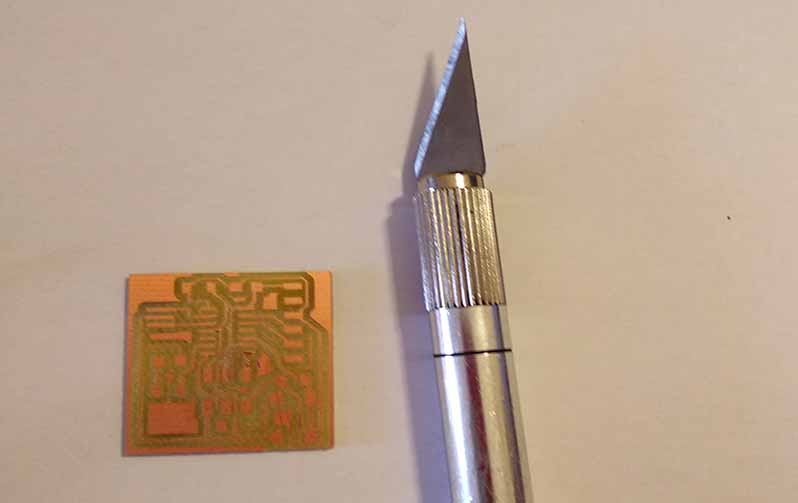
Utility knife used to fix the short circuits
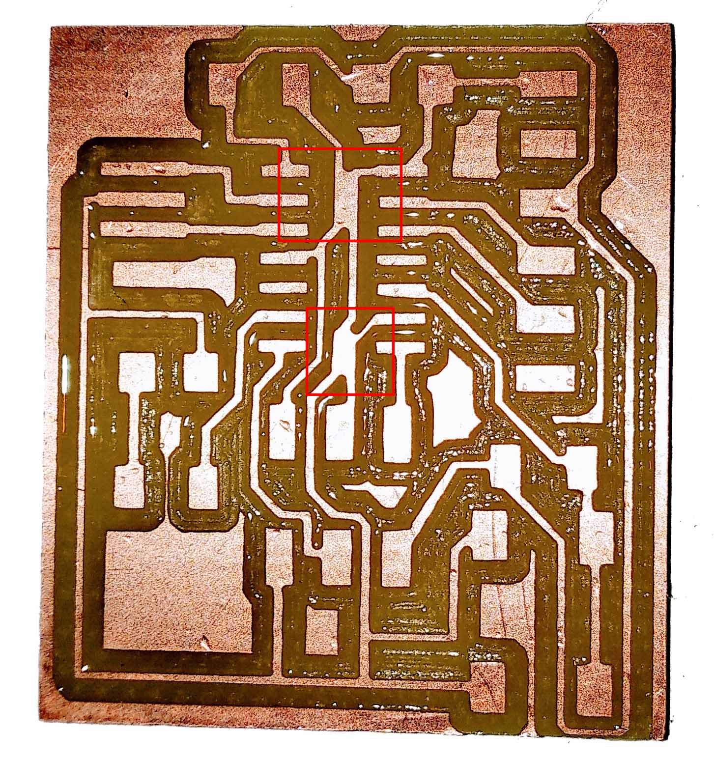
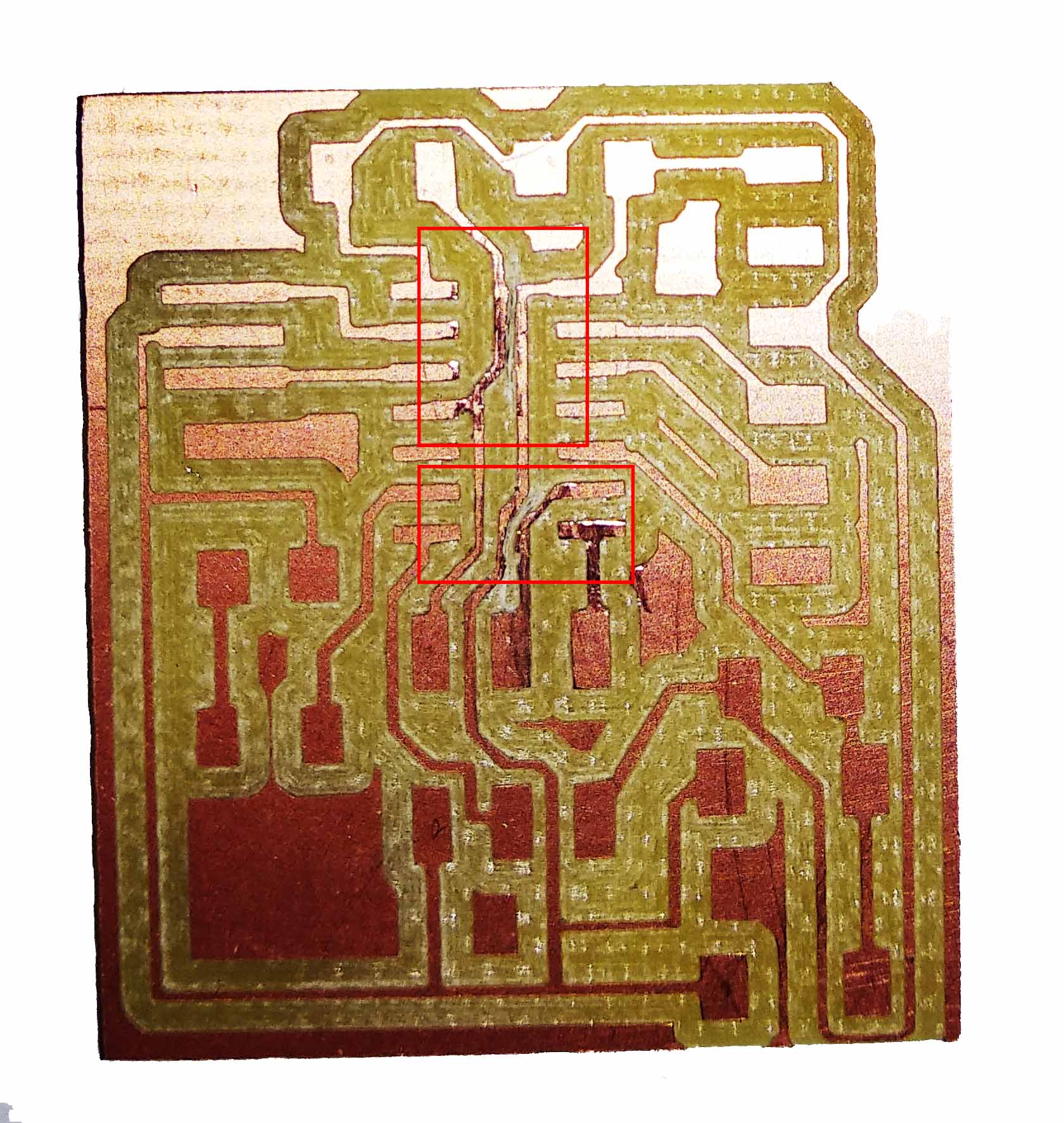
Two short circuits found
Two short circuits fixed using the utility knife
After testing and making sure that all the connections are right, I started soldering the PCB
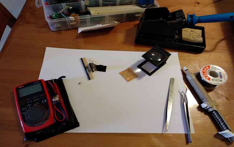
soldering hello-echo-board
Final Result
Step5: Extra credit : Render the board
I tried rendering by using the fusion sunc option in Eagle that creates a 3D file of the board
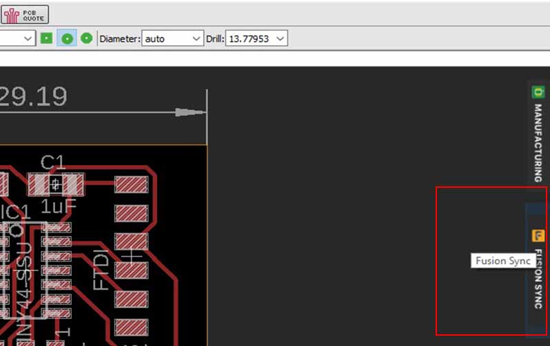
Pressed on fusion sync then create new fusion design.
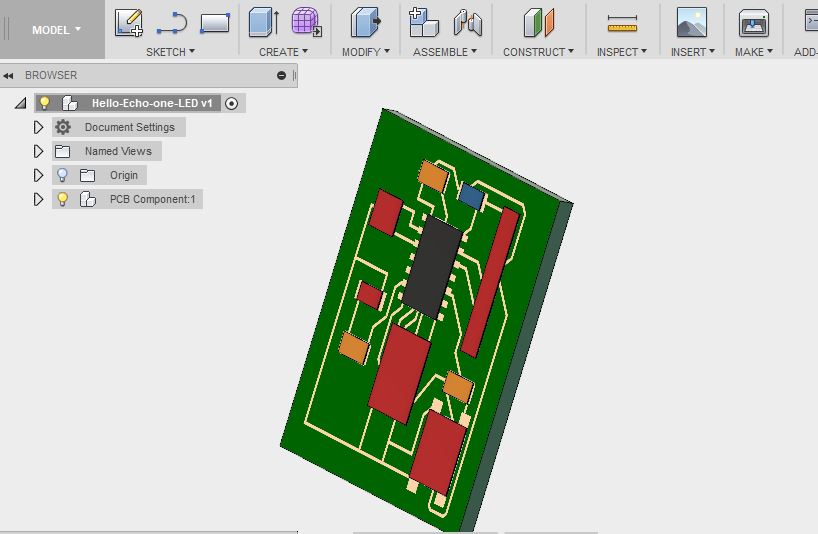
The 3D hello echo file in fusion
Errors appeared on the 3D packages while trying to render. This means that the component on fab library don't have the 3D package design. That's why the components don't have their actual shape on fusion.
Step6: test the board
- connect the hello echo to FAB ISP
- Make sure that the board is recognized by the computer
- Try testing the board by uploading hello echo code
- Check the AT-tiny44, crystal,ISP header and FTDI headers that they are well soldered.
- Check that all pins are connected according to the layout.
- Check that there is no shortcircuits
- Check that there is a power recieved on the board by measuring the voltage between the VCC line and the Ground line.
- Try Programming using Arduino as an ISP
- Program using Fab ISP
- Check Serial communication
- You have to be sure that the proper driver is installed otherwise the computer will not be able to recognize the FTDI
- For my board Rx is connected to Rx and Tx is connected to Tx but this depends on the cable or the board you have, Some times Rx is connected to Tx and Tx is connected to Rx
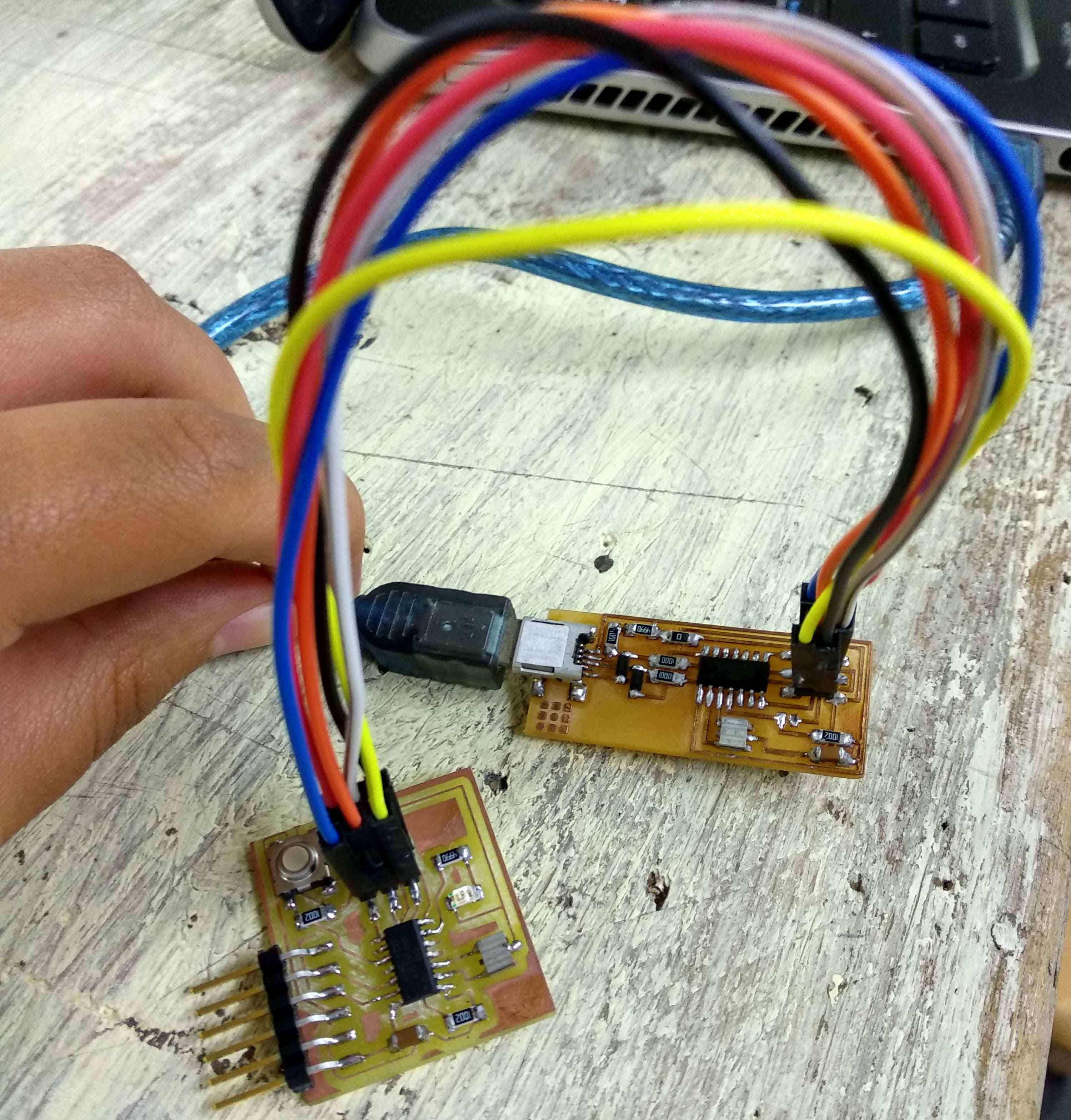
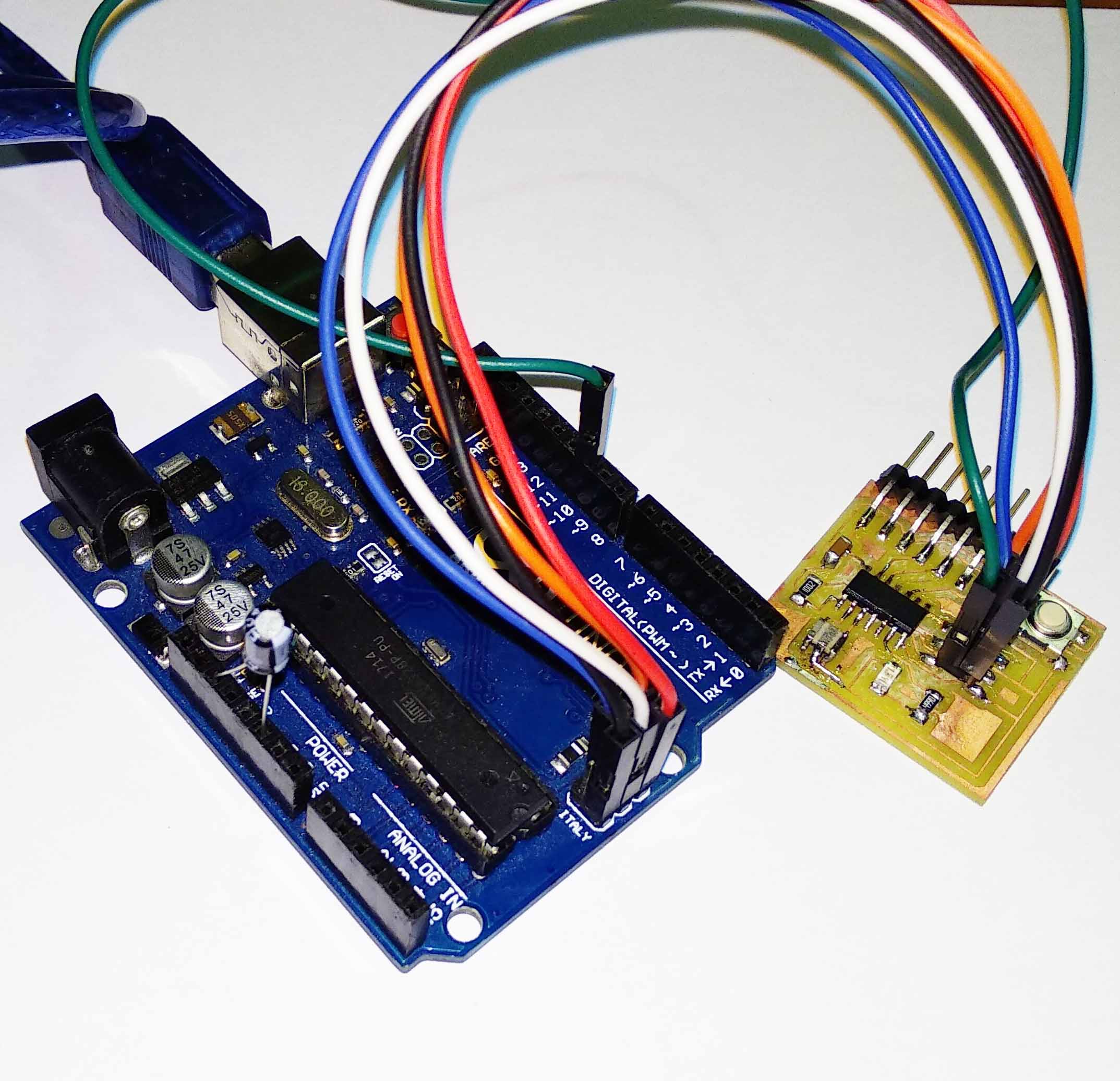
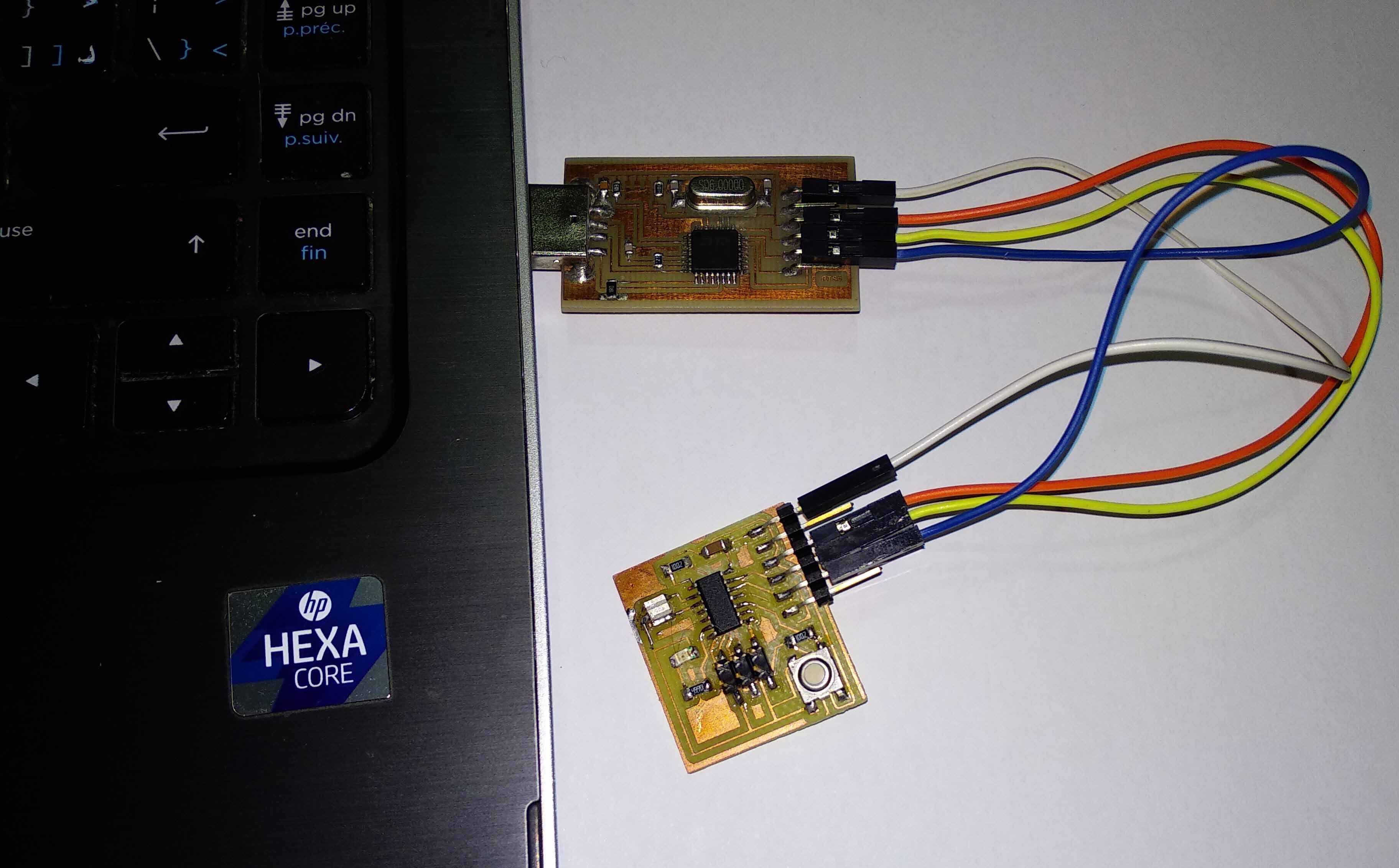
We will upload a test code to the hello echo through the FAB ISP programmer we made atweek 4.
I connected every pin on Fab ISP board to it's coressponding on Hello Echo board and then connected the Fab ISP to my computer
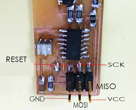
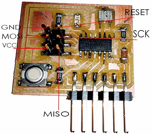
FAB ISP header pinout
Hello Echo header pinout
Hello echo board connected to Fab ISP connected to computer
When I connected the Fab Isp to the computer it should be recognized but when I opened the Device manager it wasnot recognized so I had to download AVR programmer and SPI interface driver for windows 7,8 and XP.
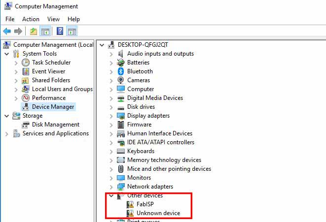
FAB ISP was not recognized on device manager
After downloading the drivers and reconnect FAB ISP it was recognized.
I downloaded the hello echo board firmware that enables the board to serial communicate with the computer.
Change the directory to the location of the firmware then type the command
make f hello.ftdi.44.echo.c.make
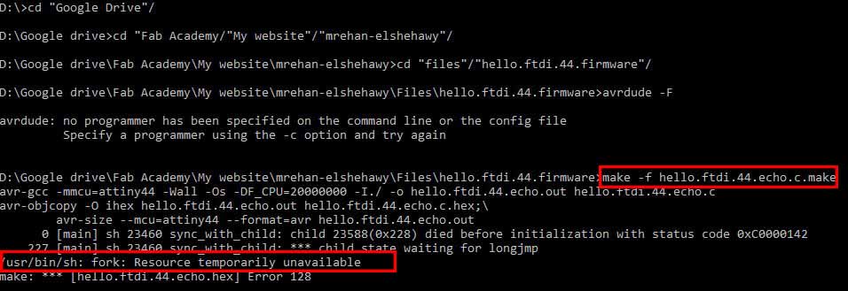
I got an error state that fork:Resources temporarliy unavailable.
After searching about the error I found a tutorial of Nathan and also this tutorial.
These tutorials stated that windows 8 has a compilation error with AVRdud and a new msys-1.0.dll file should be installed and should be put on C:\WinAVR\utils\bin
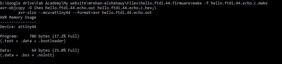
After installing the new .dll file and redo the previous step make command was successful
The next step was to write make -f hello.ftdi.44.echo.c.make program-usbtiny-fuses.
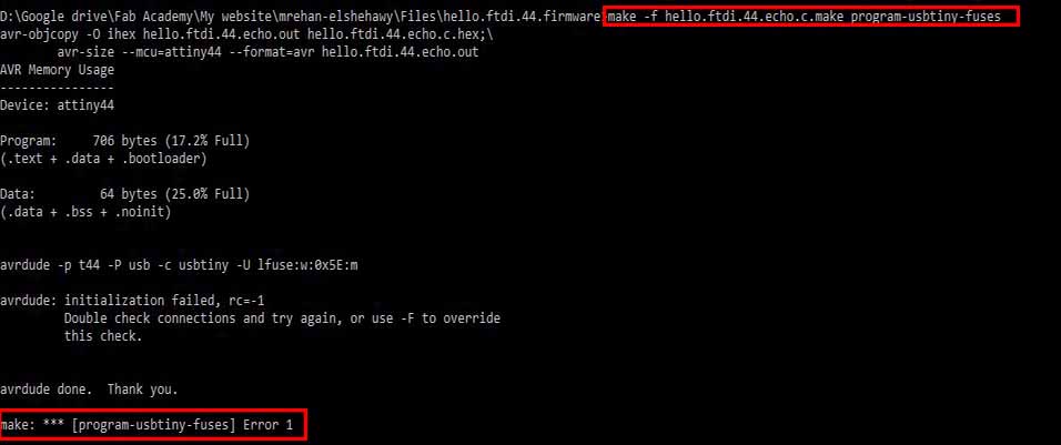
I got a new error states that [program-usbtiny-fuses]Error1
This is the check that I made
After that the error was still the same so I decided to try programming the hello echo with arduino board. If it was programmed then the error should be on my Fab ISP. If it was not programmed, Then the error should be in the board itself.
I found this Programming Attiny with Arduino tutorial that was actually really helpful and I followed the steps on it.
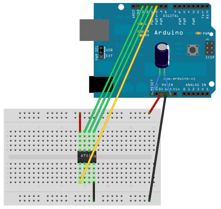
The Attiny should be connected to arduino on this way. Actually it's the same as the connection on week4
I connected the same but using the ISP header and female to female jumper wires.
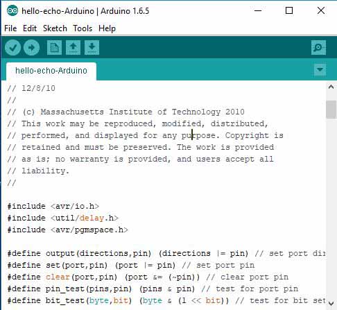
I opened the .c file with a text editor and copied the file then paste it on arduino IDE
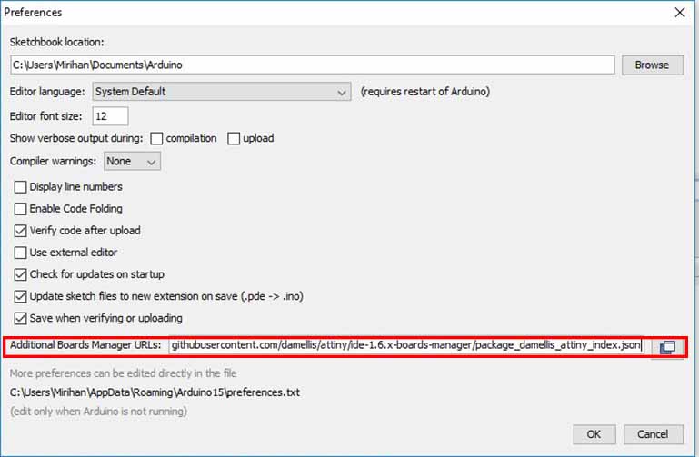
From file>prefrences add https://raw.githubusercontent.com/damellis/attiny/ide-1.6.x-boards-manager/package_damellis_attiny_index.json in the additional boards managers URLs
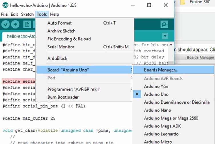
From tools>Board select board manager
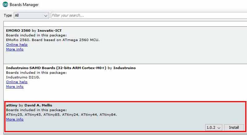
From board manager search about Attiny and install it.
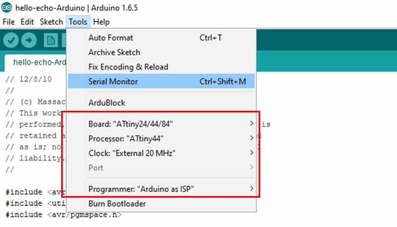
From tools select the Board Attiny24/44/84, Processor Attiny44, Clock External 20MHZ and programmer Arduino as ISP.
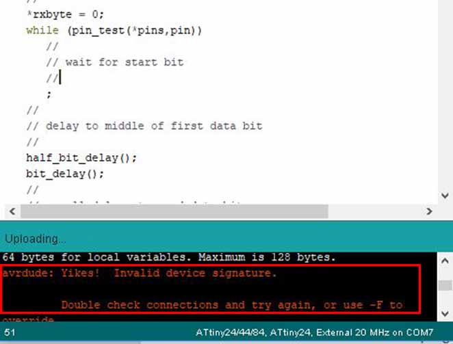
When I uploaded the code I got the same errorAvrdud: Yikes! Invalid device signature
I went to prefrences and checked on show verbos output during compilation and upload to show more details about the error. The error was device signature 0x000000. When I searched about the error I found that this happens if the programmer can't read the attiny due to clock error. So I changed the clock and rechecked the Attiny soldering.
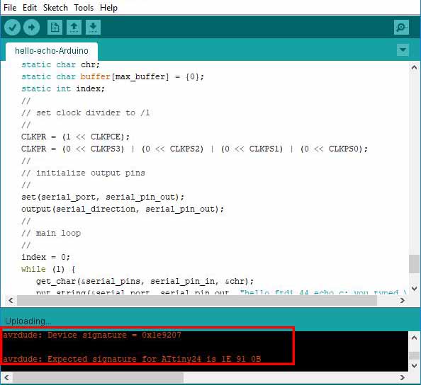
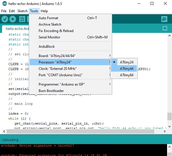
Afterthat I tried to upload the code again, It gave me a device signature finally but it was for Attiny 24. I must have changed the processor by mistake during the debugging.
I re selected Attiny 44 from the tools.
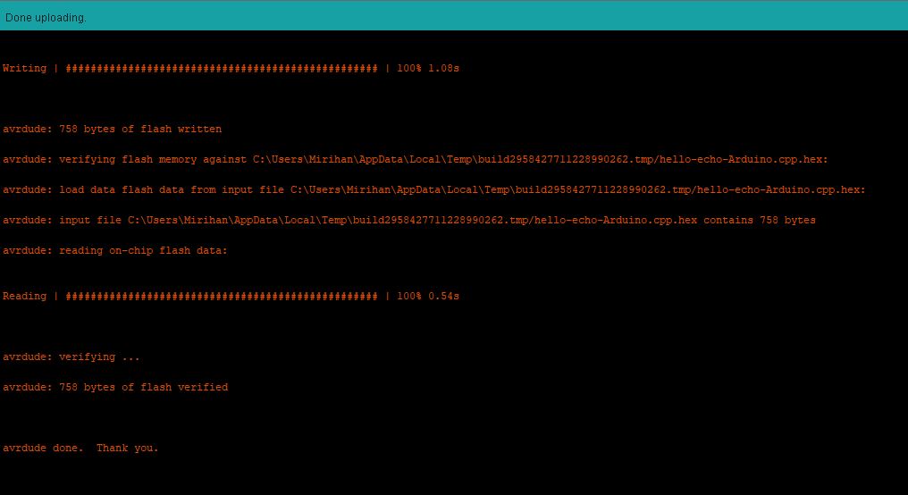
uploade successful . Haleloiaaaaa.
reconnect Fab ISP to hello echo then reprogram using the following commands
    make -f hello.ftdi.44.echo.c.make
    make -f hello.ftdi.44.echo.c.make program-usbtiny-fuses
    make -f hello.ftdi.44.echo.c.make program-usbtiny
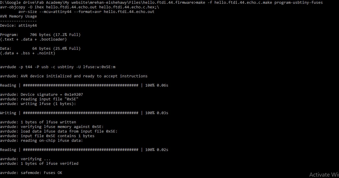
Fuse ok!
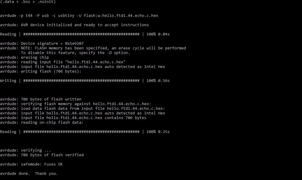
Programming is done!
The test code I uploaded use the serial communication to act as an echo of what we type on the serial monitor. If this worked will it means that the board is functional, has no errors and can be successfully programmed for any other function.
To connect the board to the computer a serial to USB interface is needed, which is known as FTDI (The name of the company that makes these interfaces).
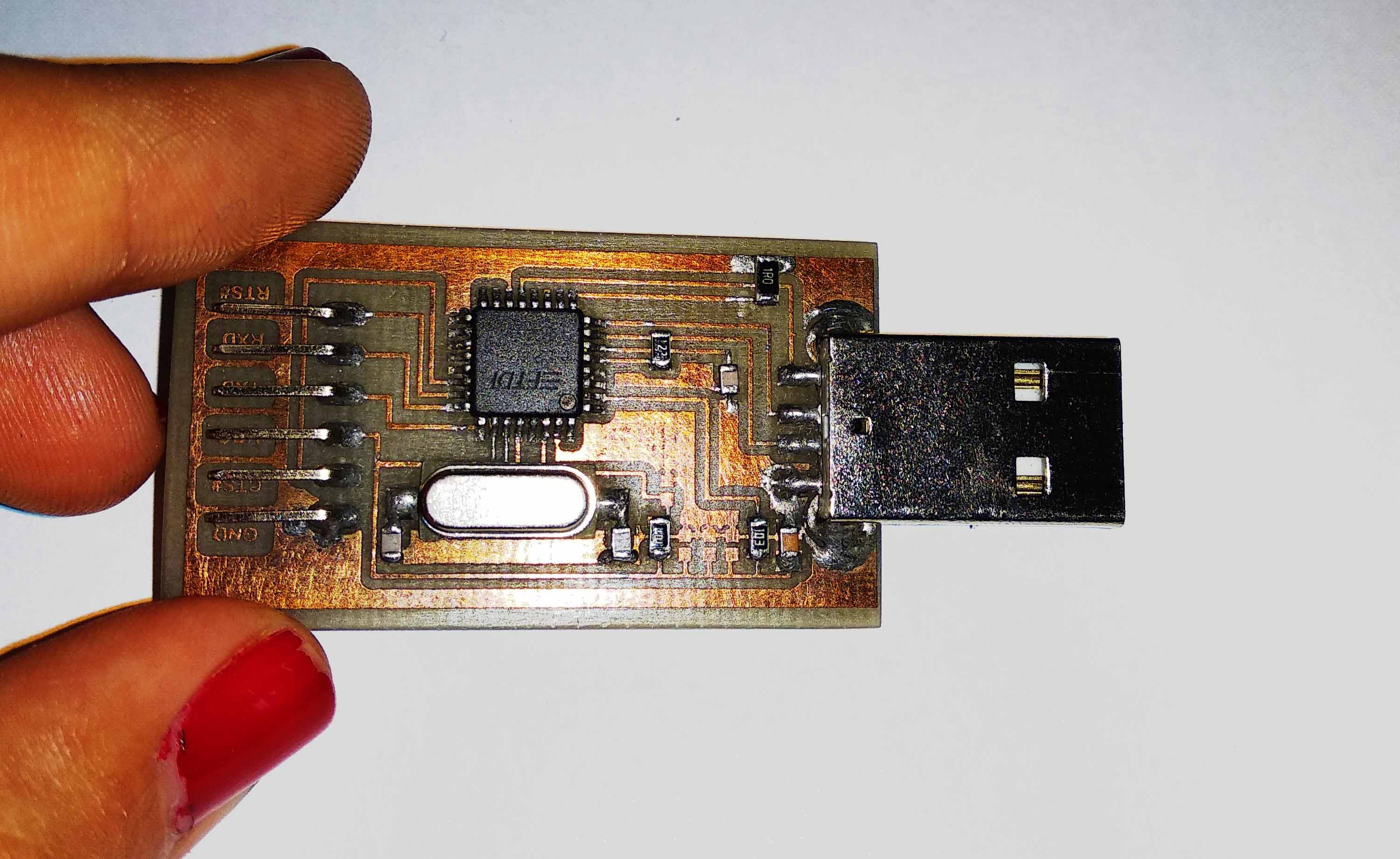
For me, I used FTDI clone board that was made by my husband
I connected the VCC, GND, RX, TX between the FTDI and hello echo board then connected the FTDI to my computer.
There are two notes that I came into while exploring the FTDI
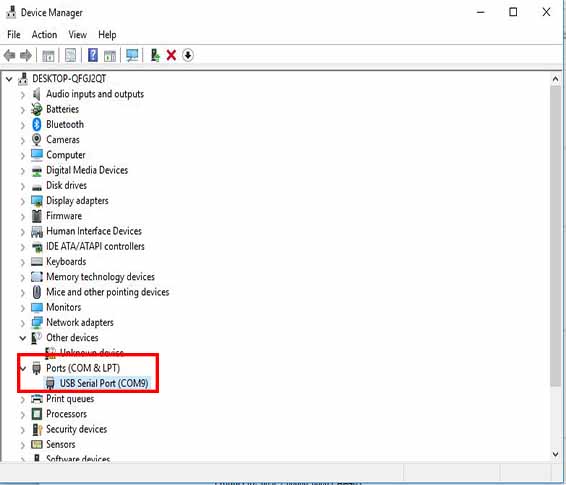
After connecting the FTDI, Check from device manager which com the FTDI is connected to.
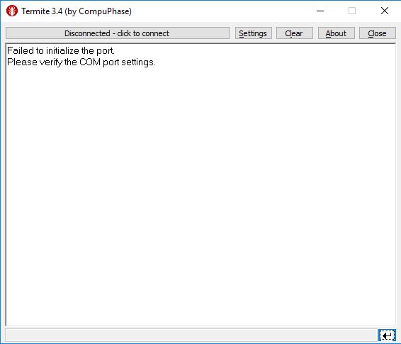
I downloaded Trime which is a serial communication terminal.
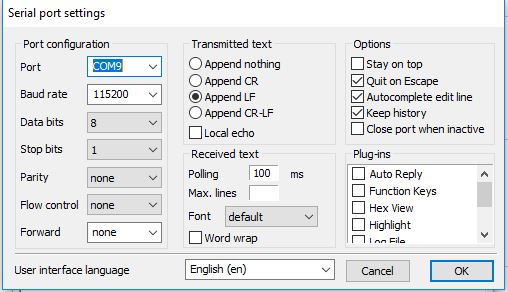
Open settings and select the right port and 115200 baud rate.
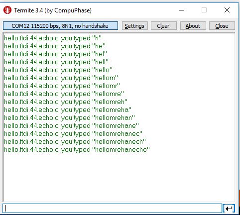
Start typing and the board will respond back with what you typed before followed by the first letter of what you typed now.
Board is working !!!
Files:
- Hello Echo with one led eagle file
- hello echo with one led traces file
- hello echo with one led outline file
Resources I used in this week:
- Fab Academy Introduction to eagle
- Sparkfun tutorial
- Testing the polarization of a SMD led.
- Jakob Nilson website
- How to link between eagle and fusion tutorial

