

Huber Girón Nieto
Electronic and Mechatronic Engineer
Contact
e-mail: huber.giron.nieto@iberopuebla.mx
phone: +52 (222) 372 3000 ext.12917
FABLAB Puebla Researcher
WEEK ASSIGNMENT:
Electronics Production
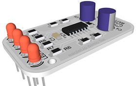
Make the FabISP in-circuit programmer
For this week activity , a printed circuit was made using FabISP programmer design , this in order to understand the manufacturing process of printed circuits, the circuit is will be used for programming AVR micro controllers.
Printed Circuit Board
In electronics, a circuit board, printed circuit board or PCB, is an area consisting of paths or tracks of conductive material laminated onto a non-conductive base.
The printed circuit is used to electrically connect through conductive paths, and mechanically hold of electronic components through the base.
The roads are usually copper while the base is made of resin reinforced fiberglass, ceramic, plastic, Teflon or polymers such as Bakelite.
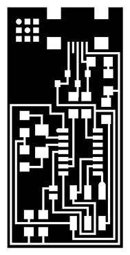
Design
The Electronics Production assignment is to mill the board, stuff it with components and program it. We will be using these programmers through the semester to program the other boards we create.
The FabISP is an in-system programmer for AVR microcontrollers, designed for production within a FabLab. It allows you to program the microcontrollers on other boards you make.
The genealogy of the FabISP design is interesting in its own right; Neil's FabISP is based on David Mellis's FabISP which is based on Limor's USBTinyISP which is based on Dick Streefland's USBTiny.
Components
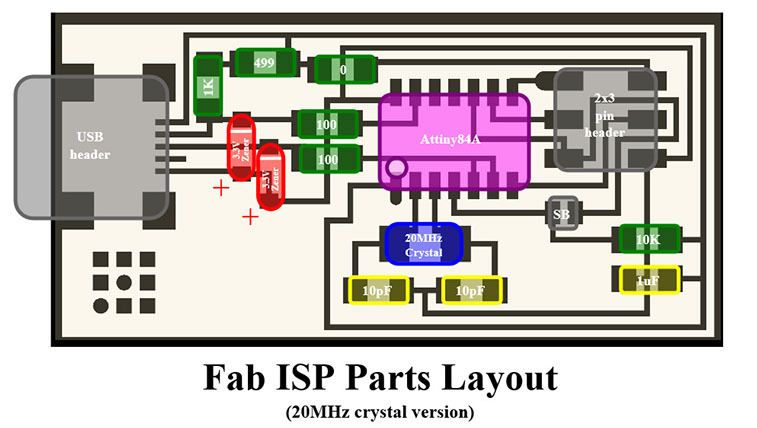
All necessary parts to build the circuit are:
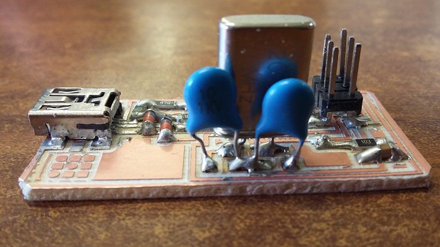
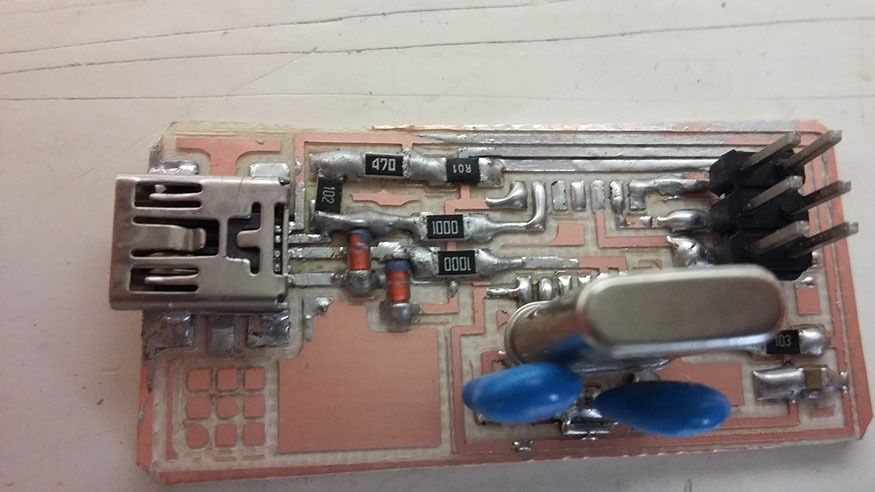
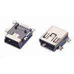
- Mini USB Header
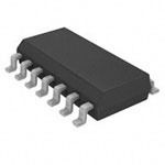
- Microcontroller : ATTiny 44
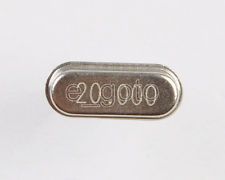
- Crystal 20MHz
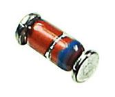
- Two Zener Diode 3.3 V
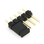
- Jumpers an 6 pin programming header
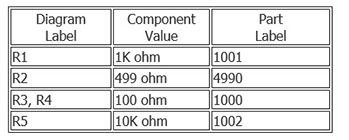
- Resistors
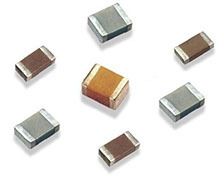
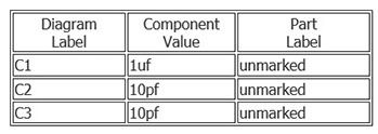
- Capacitors
To achieve the various components, we investigate and check the availability in electronics stores nearby to FabLab and the city of Puebla and even in various stores in Mexico using Internet.
However, we don't obtained all components according to the list, it was especially difficult to get SMD components, finally most of SMD components were buyed, except capacitors and crystals, because we only obtained those in through hole version.
We could not find the micro-controller available in Mexico, so it was necessary to apply a request in a delivery period of one week. Therefore, in this activity was not possible to complete the circuit as explained below.
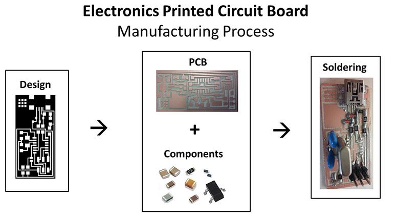
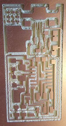
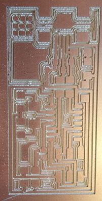
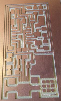
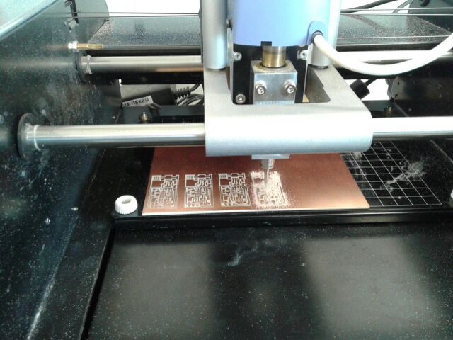
PCB Fabrication
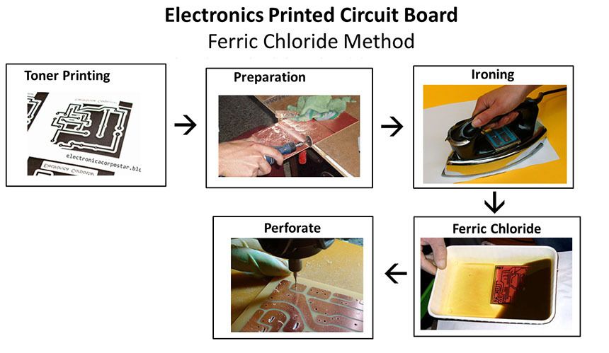
Make printed circuit boards is not something new for me, since I am Electronic Engineer, however always had done by the method of ferric chloride, which is a very slow and dirty method, make a circuit can take from one to two hours.
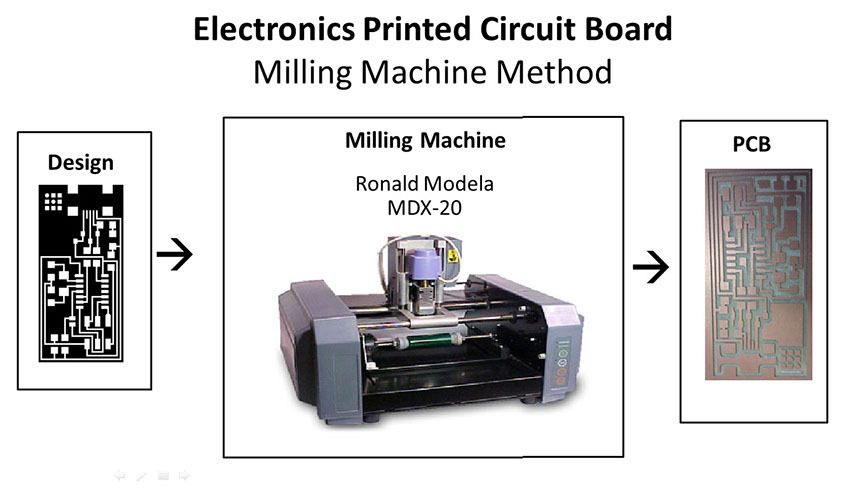
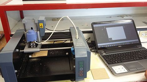
Now in this assignment, we used the tutorials to develop PCB with the help of a milling machine, so that the process becomes very fast and much cleaner.
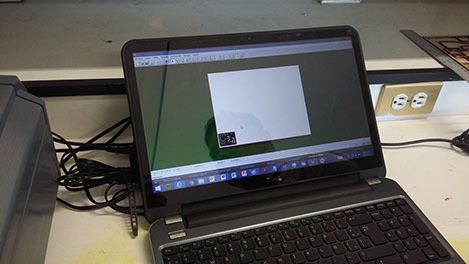
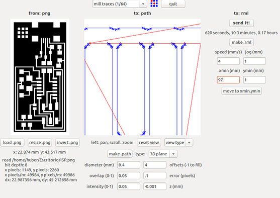
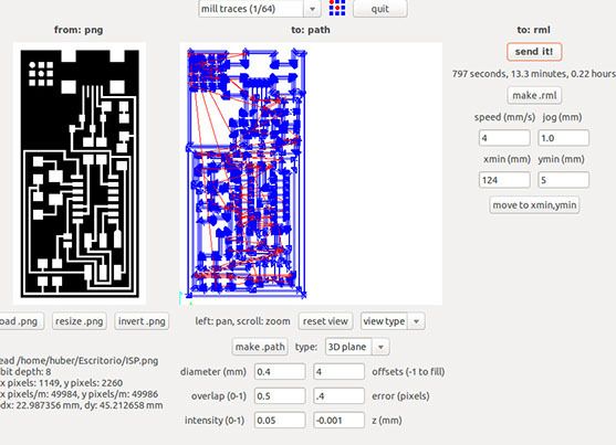
In the tutorials to use the Modela in PCB manufacturing, mentions that you need to install Fab Modules on a machine with Linux based OS, however, in Fablab Puebla everyone uses Windows operating system so the Fab Modules were ignored as a first option, we decided to use software brings the machine by default: Dr. Engrave.
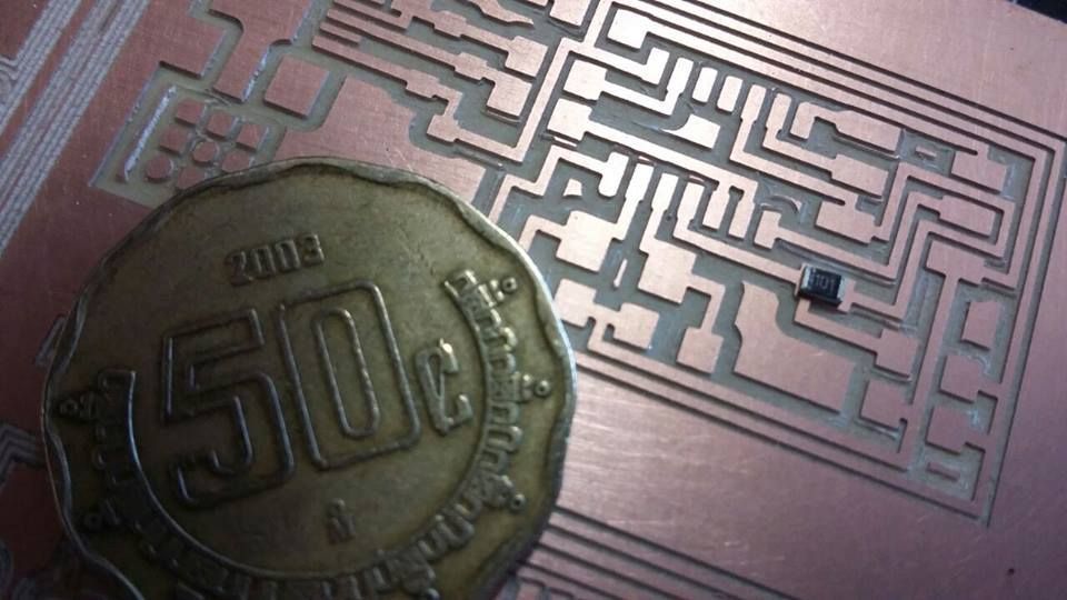
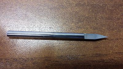
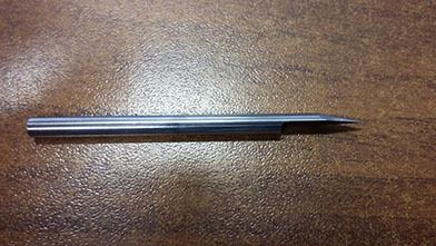
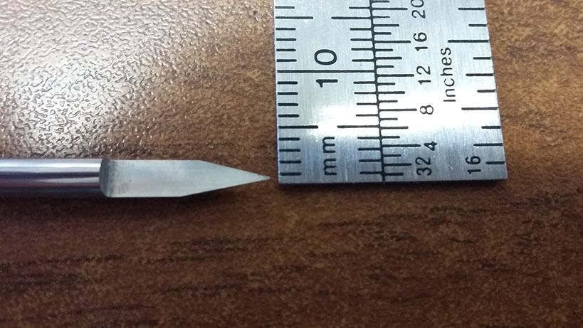
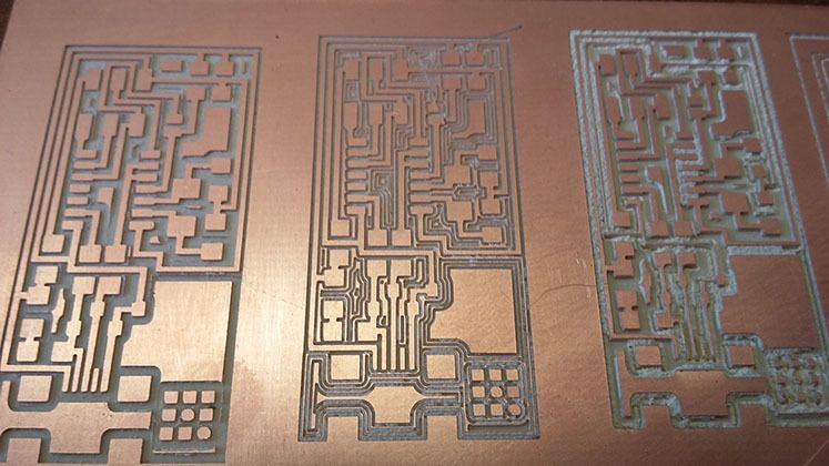
We use a cutting tip tool because it was available at the moment , however we realized it was the best option, because the tip allowed to have a higher quality engraved circuits.
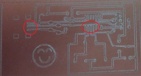
Several tests were performed by varying the parameters of engraving depth, however several of the circuits tracks were damaged . Then it was discovered that the program Dr, Engrave only vectorized circuits and then only follow the contours damaging the tracks.
A see these tests performed unsatisfactorily, We decide to have a computer with Ubuntu to install Fab modules
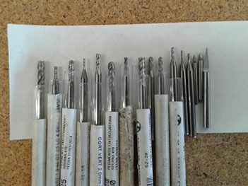
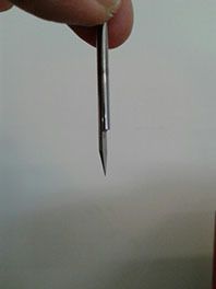
Carbide Steel 30 Degree 1/8" CNC Router Triangular Pyramid Engraving Bits
The installation of "Fab Modules" turned out really complicated, especially because as I mentioned earlier, we had not experience with Linux platforms and we were accustomed to windows executables.
It was important to know the Linux terminal since this was the main tool for installation an it was also subsequently necessary to installing the printer on Ubuntu.
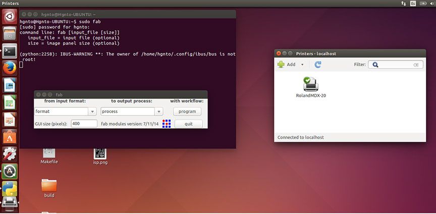
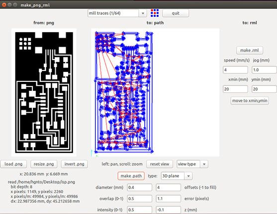
Once executed Fab Modules, the environment is very intuitive and perform various tests by varying the parameters of depth, speed, resolution and others. Finally we obtain certain end values for the parameters.
PARAMETERS RESULTS
Soldering
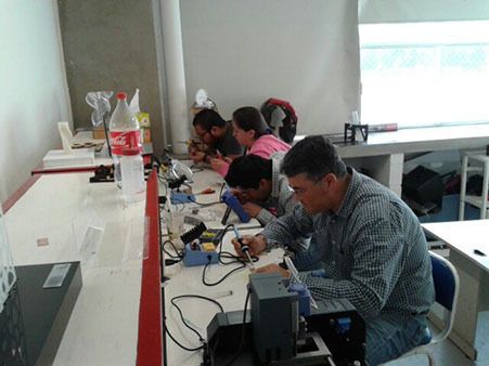
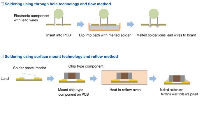
Finally, once made the PCB´s, we solder SMD components, in addition to making adjustments for Through-Hole components.
However it was not possible to complete the circuit because we don't have the ATtiny44A microcontrollers.