Helmut Uwe [OOVAE] Terton - Fab Academy |
||
Helmut Uwe [OOVAE] Terton - Fab Academy |
||

Assignment tasks for Week 6:
Group assignment
Contents
We have two devices for testing electronic devices: a Multimeter and a USB Oscilloscope.
Fluke 85 Multimeter
Specifications & Description:
DC Min (Volts)0.4
DC Max (Volts)1000
DC Voltage Accuracy±0.08% of reading + 1 digit
DC Min (amps)0.00039
DC Max (amps)10
DC Current Accuracy±0.2% of reading + 2 digits
AC Min (Volts)0.4
AC Max (Volts)1000
AC Min (amps)0.0004
AC Max (amps)10
AC Current Accuracy±1.0% of reading + 2 digits
Resistance Min (?)400
Resistance Max (M?)40
Capacitance Min (nF)5
Capacitance Max (mF)5
Frequency Min (Hz)199.99
Frequency Max (KHz)199.99
Safety RatingIEC 1010-1, 1000 V CAT III
Power9 V battery (included)
Width (in)3.5
Height (in)7.33
Depth (in)1.25
Description Industrial Multimeter 600V
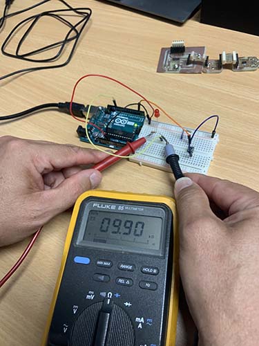
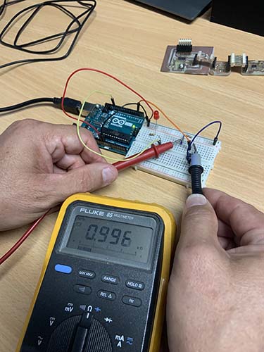
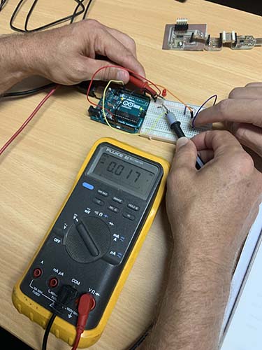
I used the Multimeter to measure the resistance of the resistors and to measure the milli Volts while in action as illustrated in the figures below.
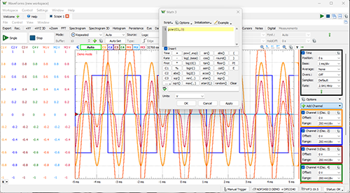
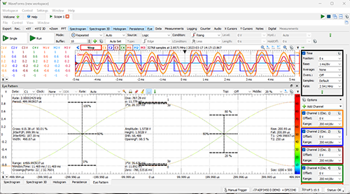
The second testing device in our lab here is Lismore is the Digilent Analog Discovery 2 PC Based Oscilloscope, 30MHz, 2 Analogue Channels.
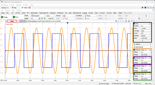
The oscilloscope was lent to me by the SCU engineering department, I played with it but it really doesn't make sense to me. It has a lot of settings and display modes as shown in the figures below. It needs a proper introduction to oscilloscope reading to fully understand the readings and the meaning behind the readings.
The readings are displayed in a software called WaveForm, which can be downlaoded for free here:
https://digilent.com/shop/software/digilent-waveforms/
Summary
I feel comfortable to use the multimeter but not using the oscilloscope. More time needs to be invested in learning the workings and usage of an oscilloscope.
Designing a PCB for the XIAO ESP32-C3
The plan is to use the XIAO ESP32-C3 for my final project.
During the tutorial we designed a board design for the Xiao ESP32-C3.
All the components needed for the board can be found at Seed Studio
https://wiki.seeedstudio.com/XIAO_ESP32C3_Getting_Started/#resources
The first step was to install the component library for the ESP32-C3 microcontroller to the KiCad library section.
The libraries for many boards can be downloaded from the Fabcloud
https://gitlab.fabcloud.org/pub/libraries/electronics/kicad
but for the ESP32-C3 I went to the Seet Studio website again.
https://wiki.seeedstudio.com/XIAO_ESP32C3_Getting_Started/#resources
In the tutorial we identified all the parts and connections needed for the board.
The ESP32-C3 was a great source of information for pin-out information.
https://files.seeedstudio.com/wiki/XIAO_WiFi/Resources/esp32-c3_datasheet.pdf
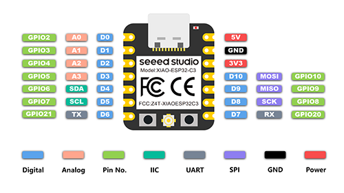
5V: Supply voltage 5V.
GND: Ground.
3V3: Supply voltage 3V3.
Digital pins (GPIO Pin number): 0, 1, 2, 3, 4, 6, 7, 26, 27, 28, 29
Analog pins (GPIO Pin number): 26, 27, 28, 29
LED Green (GPIO Pin number): 16
LED Red (GPIO Pin number): 17
LED Blue (GPIO Pin number): 25
SDA (GPIO Pin number): 6
SCL (GPIO Pin number): 7
RGB LED_POWER (GPIO Pin number): 11
RGB LED (GPIO Pin number): 12
And also watching a video on the PCB 32 design on Youtube by Phil's Lab was very insightful
https://www.youtube.com/watch?v=yxU_Kw2de08
During the tutorial Ahmed gave us a very good introduction into the workings of KiCad.
First step was designing the schematics of the board using KiCad's Schematic Editor.
The main tool we used was the Add a Symbol tool.
This tool lets you select all the components necessary to build the tool, such as resistors, capacitors, leds, micro processor and connectors.
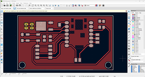
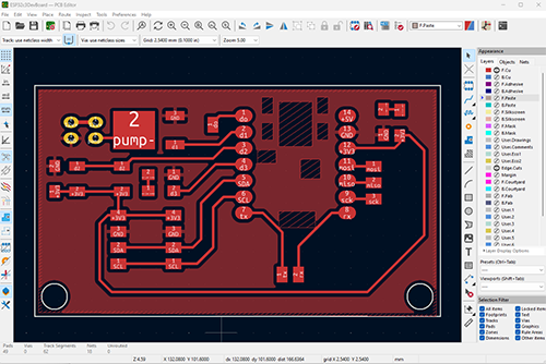
Below is the finished version of the ESP32-C3 schematic.
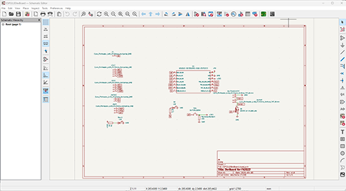
Applying the footprint assignment tool can tell the user if links are missing. In my case links to the switch button were missing and had to be added.
Summary
If it would not have been to Ahmed, I would not have been able to put a schematic or finished PCB layout together in KiCad. By no means am I an electronics expert, I never learned about electronics in school or elsewhere. It is a steep learning curve for me. I think I now grasp the basics of electronics and what the different components do, but not fully.
A lot more learning and research on the topic needs to happen.
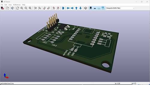
Under guidance I am now able to create a schematic and PCB layout in KiCad.
It will be interesting to see if it actually will work.
Files
ESP32c3DevBoard.kicad_pro
ESP32c3DevBoard.kicad_sch
ESP32c3DevBoard.kicad_pcb