Electronics design
This week is about learning how to design a PCB.
Contents
- Using test equipment
- Redraw a hello board
- References
- Design Files
1. Using test equipment
Using the test equipment in the lab to observe the operation of a microcontroller circuit board.
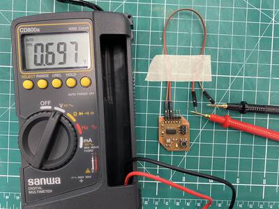
I used my hello board for this task. This tutorial on How to use a multimeter is a good resource.
A multimeter is a handy piece of equipment used for measuring voltage, current, resistance and continuity.
To measure Voltage:
Plug the black and the red probe into corresponding ports (depending on the model of multimeter).
Set the knob of multimeter to V.
Touch the black probe to the GND pin and the red probe to the VCC pin of the board.
The screen will display the voltage across GND and VCC.
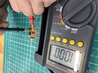
To measure Resistance:
Set the knob of multimeter to R or Ohm symbol. Use range button to select M ohm, Kilo Ohm or Ohm.
Touch the black and red probes to the two ends of any resistor on the board or the corresponding traces.
To measure Current:
Current measurement for electronic circuit board is not very common, especially for surface mount circuit boards. To measure current, the flow of current must be physically interrupted and the multimeter must be connected in-line. This can be done by adding a jumper bridge in the design of the board.
Then by connecting the two probes of the multimeter in-line to the two jumper pads on the mA setting.
To check Continuity:
Continuity testing measures the resistance between two points. If the resistance is very low, there is a beep which means the two points are in continuity. If resistance is high, the circuit is open, and the multimeter won’t beep.
This is the most useful to check connections and solder joints between microcontroller pins and header pins to connect inputs or outputs.
Set the multimeter to ‘Continuity’ - a diode symbol with propagation waves around it.
Touch the two probes on the two points to be checked and beep will give the feedback.
An oscilloscope, o-scope or scope is useful to measure amplitude, frequency or transient signals that a multimeter cannot catch. It samples a signal and displays the waveform on a screen. Both digital squarewaves and analog curved waves.
Parts of the oscilloscope interface:
1. The screen on the left displays the waveforms.
2. The channel ports. This one has 2.
3. The vertical sections controls the voltage scale on the display for each channel independently.
4. The horizontal section controls the timescale for both channels.
5. The third section is to trigger specific controls of the scope.
6. The menu section has various settings, like capturing an image for eg.
7. Buttons to start and stop measuring.
8. Passive voltage scope to measure voltage across the probe ends.
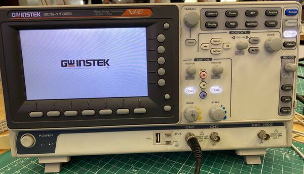
This tutorial on How to use a oscilloscope is very helpful.
As described I first make these adjustments to put the scope into a standard setup:
1. Turn channel 1 on and channel 2 off.
2. Set channel 1 to DC coupling.
3. Set the trigger source to channel 1 – no external source or alternate channel triggering.
4. Set the trigger type to rising edge, and the trigger mode to auto (as opposed to single).
5. Make sure the scope probe attenuation on the scope matches the setting on the probe (e.g. 1X, 10X).
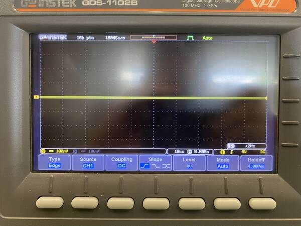
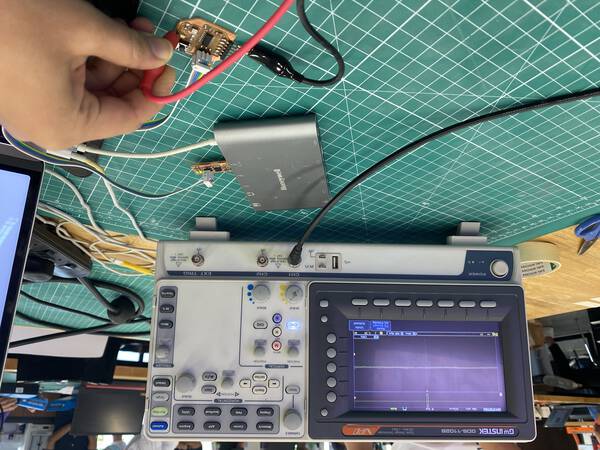
Next, I first tried to test the probe. The scopes has a built-in frequency generator that emits a reliable, set-frequency wave - there is a 1kHz square wave output at the bottom-centre of the interface. The frequency generator output has two separate conductors – one for the signal and one for ground. I connected the probe’s ground clip to the ground, and the probe tip to the signal output.
As soon as I connect both parts of the probe, I see a signal begin to dance around the screen. I fiddle with the horizontal and vertical system knobs to scale and position the waveform on the screen with a visible zoom level.
I adjusted the screw on the probe handle until I have a straight-edged square wave.
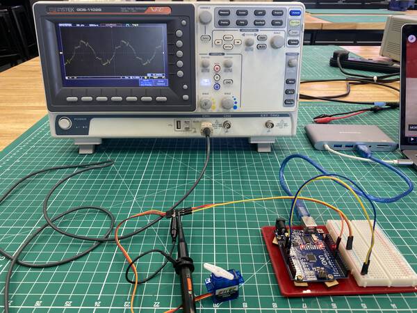
Finally, I used an Arduino Uno with a blink program on external LED to check output signals. By connecting the probe to GND and output pins, and adjusting the visible waveforms, horizontal and vertical scale and position, I found a dancing waveform like in the picture:
If this equipment is not available, another way to test microcontroller circuit boards is by making a simulation in web-apps like TinkerCAD or the open-source Arduino simulator, Wokwi.
2. Redraw a hello board
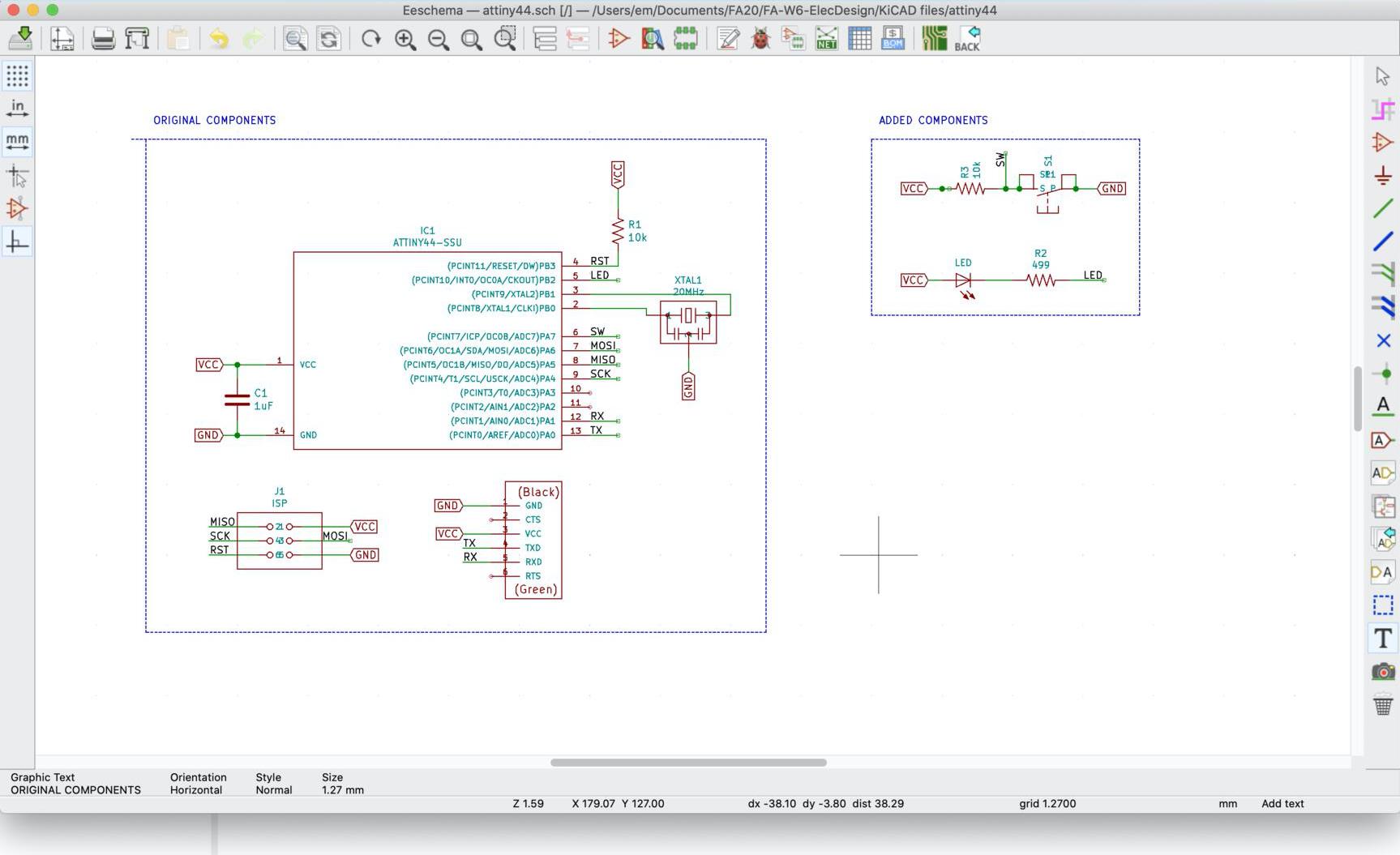
I chose a hello.echo board based on ATtiny44 as it has the most available documentation.
Here is what the actual board looks like

To add an LED and a switch, I started by making a list of the components required:
Components list:
1x ATtiny44 microcontroller
1x 1uF Capacitor
1x header 2x3
1x FTDI connector
1x 10k ohm resistor
1x 20MHz resonator
Added components:
1x LED
1x 1kΩ Resistor
1x switch
1x 1kΩ Resistor
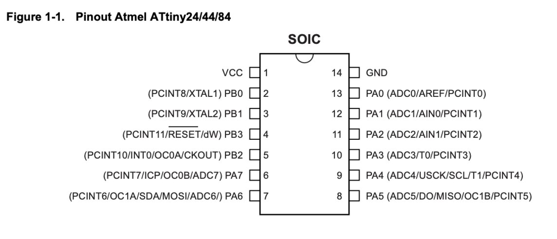
Data sheet for ATtiny44 - You can find an explanation in the Embedded Programming week.
Pinout for Attiny44:
Creating the schematic
I used KiCad 5.1.6 to design my PCB. KiCad is an open source software suite for Electronic Design Automation (EDA). The program helps create a Schematic in sub-application called Eeschema, and then design the PCB Layout with Gerber output (this is what you send to a manufacturer) in another sub-application called PCBnew.
Update libraries
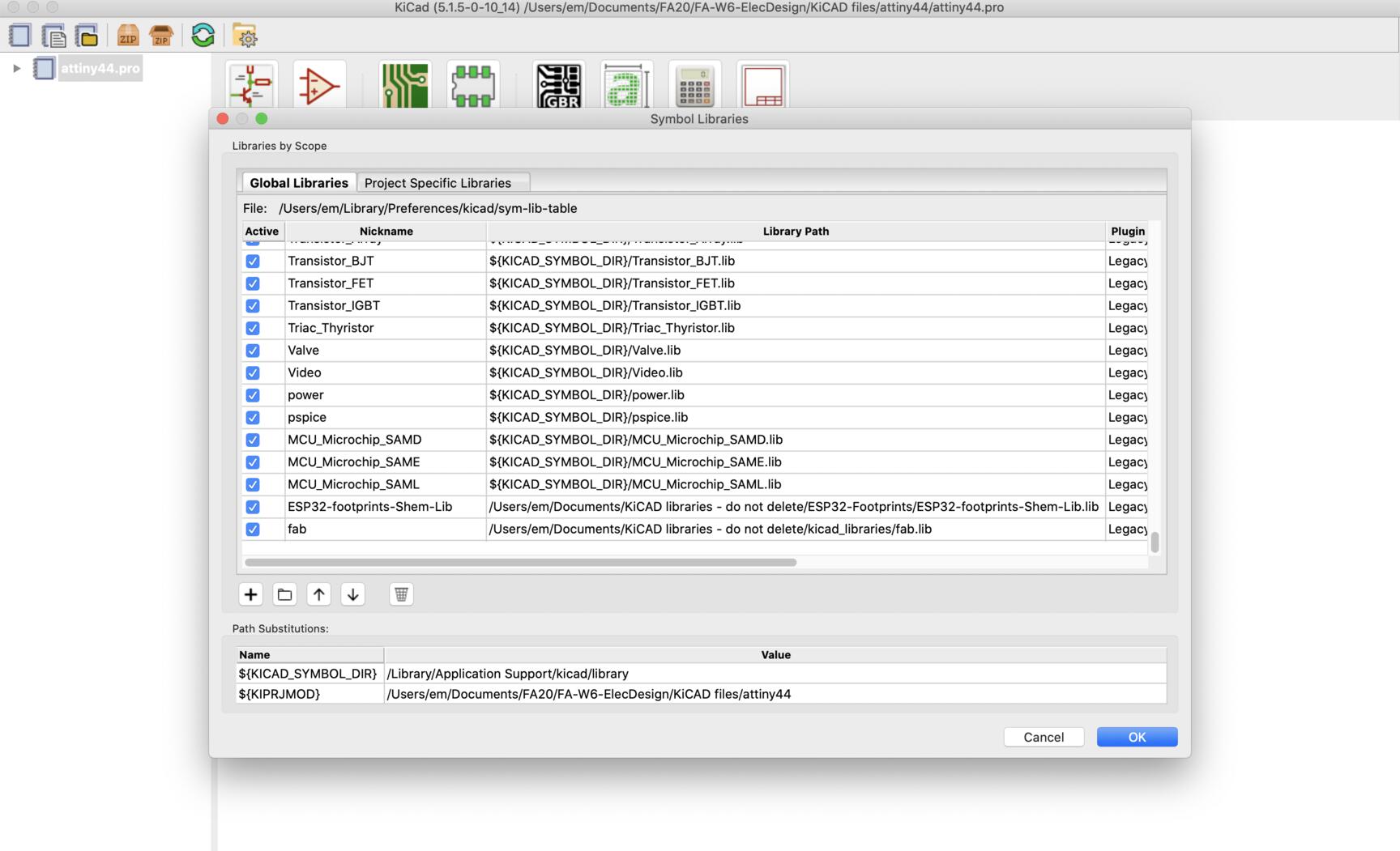
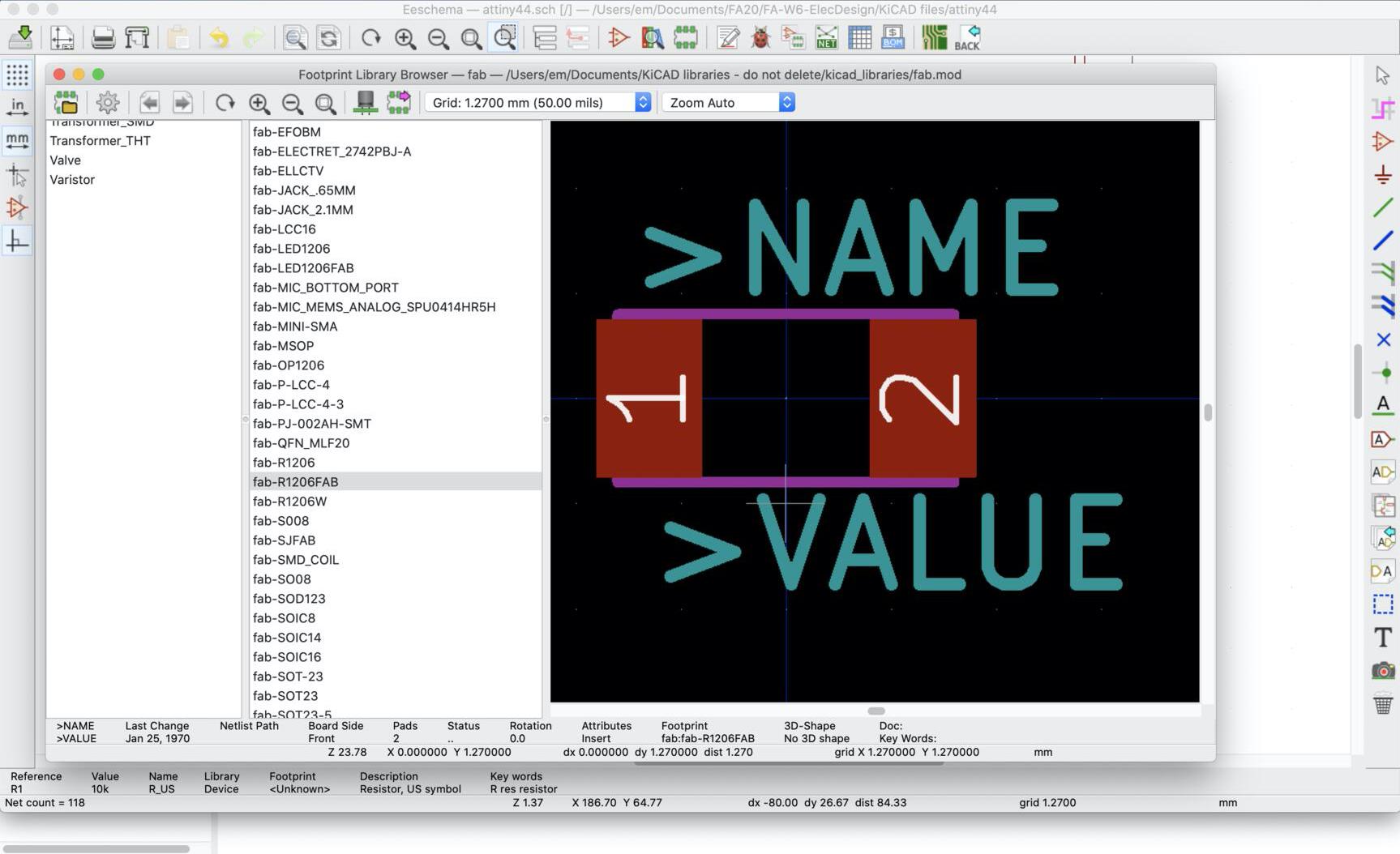
First step is to import all of the symbol and footprint libraries adapted for SMD components. These libraries can be found here.
Designing schematic
I placed the components listed above one by one, using the place component tool. Then changed properties like annotations and values, by hovering above the component and pressing E which opens the symbol properties window.
I also placed some tags using the tag tool - like GND and VCC, to make the schematic neat and clear.
Finally, I generated a Netlist by pressing the green netlist symbol on the toolbar.
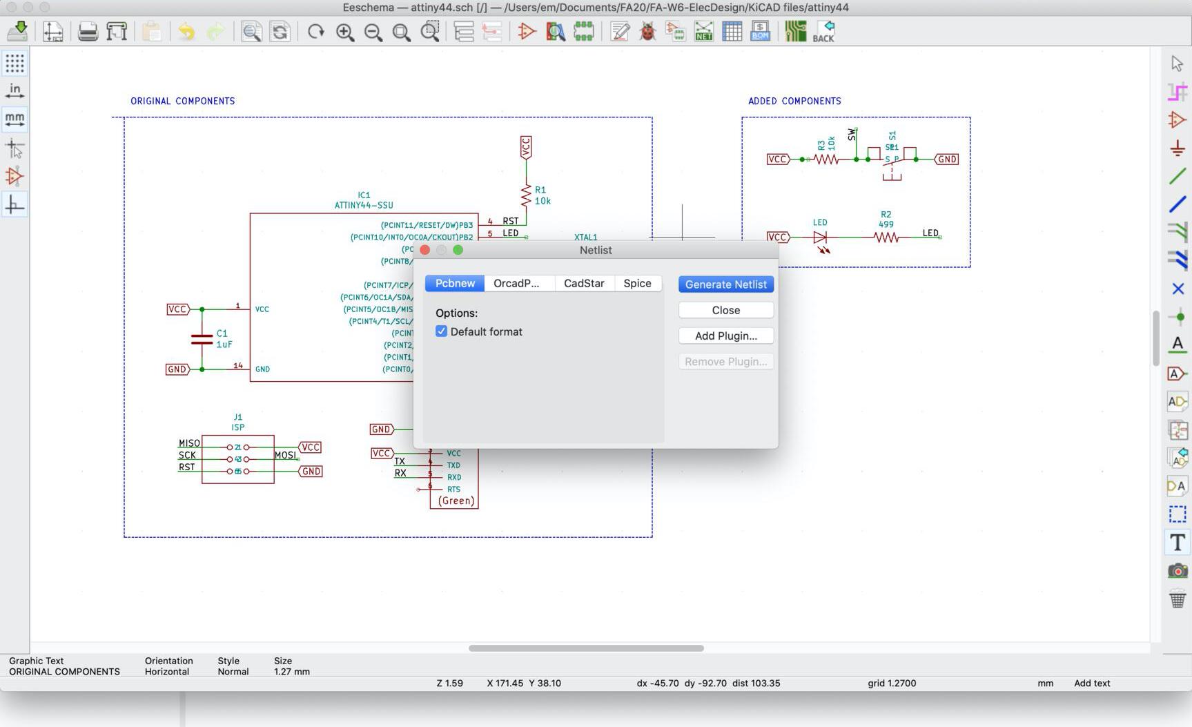
However I got an error saying that component R1 did not have footprints defined.
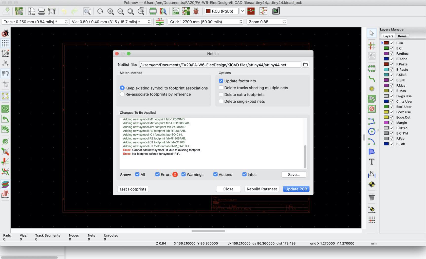
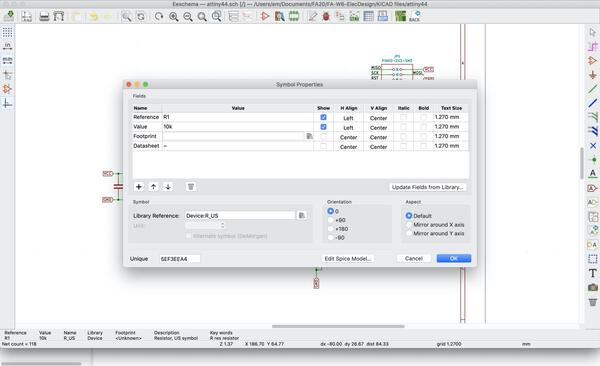
So I went back and assigned footprints to the missing part, by going to its properties again, and selecting the correct footprint from the newly installed libraries. And generated the netlist again.
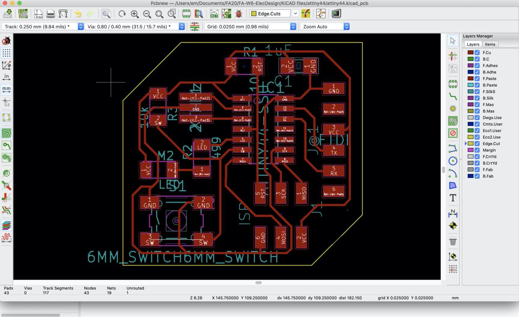
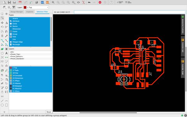
Drawing traces
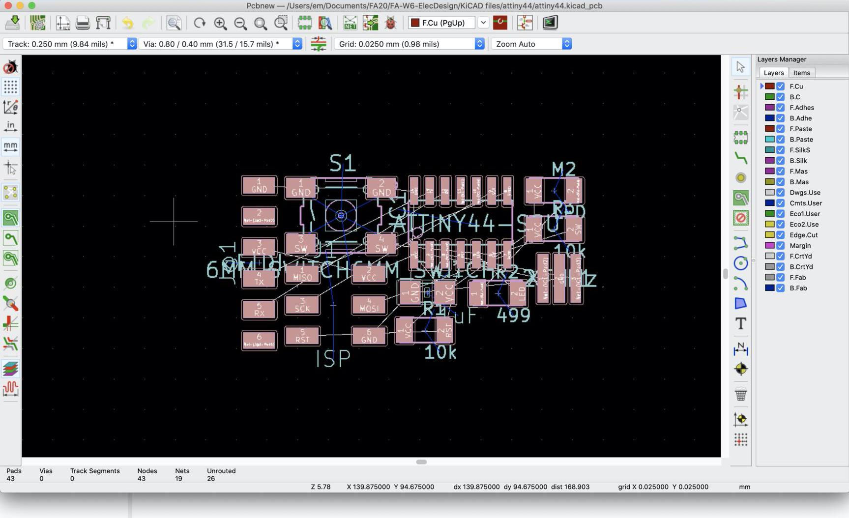
Then I opened the KiCad pcbnew part, and loaded the netlist and stacked of all components in the middle of the board.
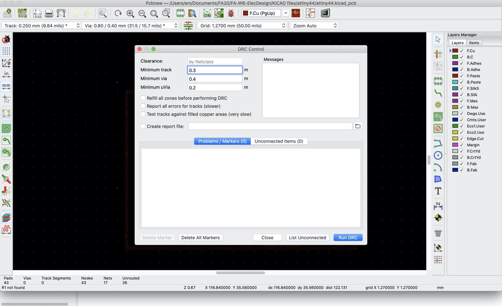
Design Rules in KiCAD: To mill the traces we use a 0.4 mm (1/64”) end-mill. Which rounds up to 0.016 inches (0.015625 inches) or 16 mil. In the Design Rules Control you can set up Net Classes and Global Design Rules. I change both the trace width and the clearance to 16 mil. I also set the grid size to 16 mil to make it easier.
The components all have an indicative line connection, so I used that to rearrange them and then added the traces, using the trace tool.
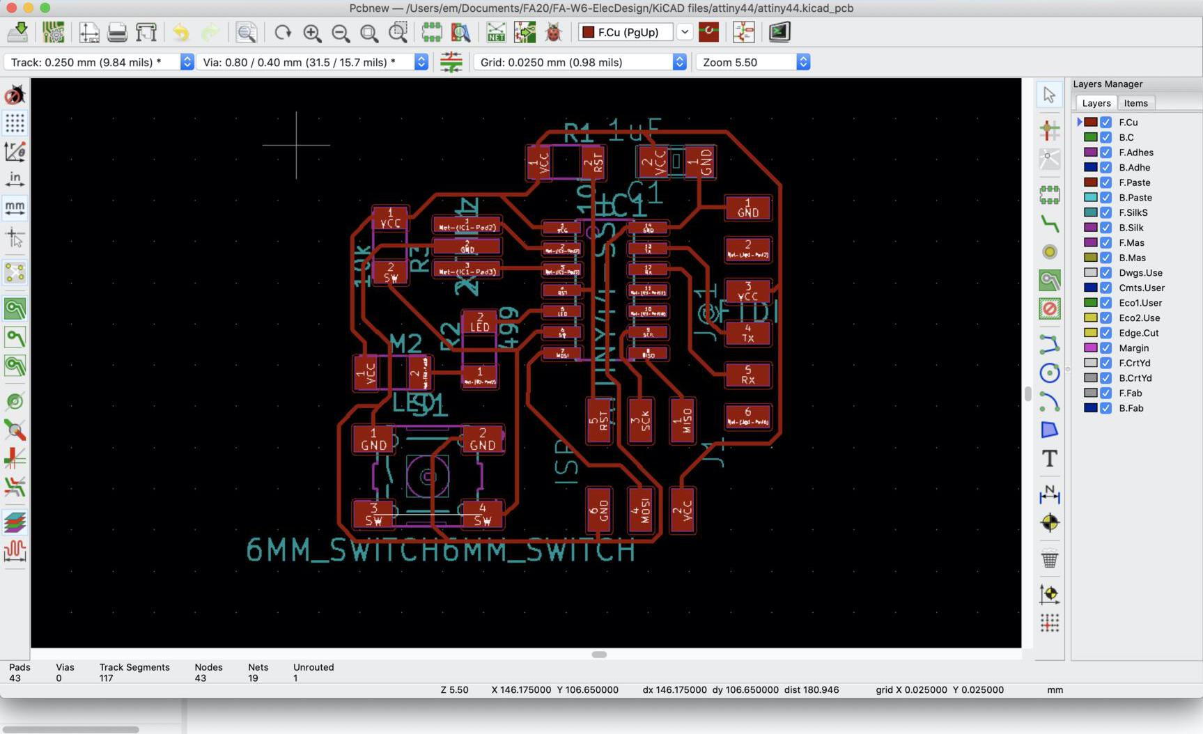
After connecting them all, I used the line tool to draw the outline like so.
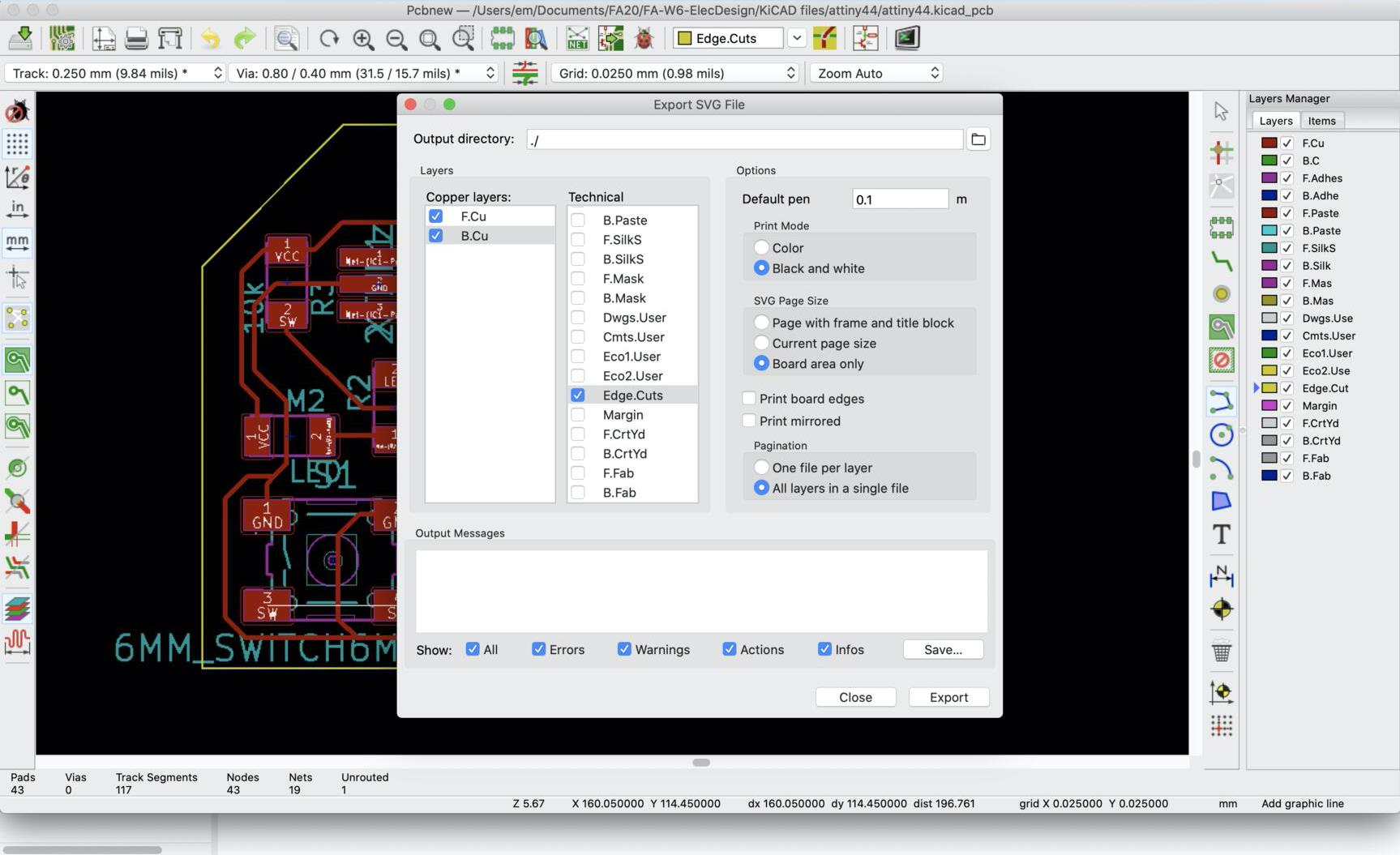
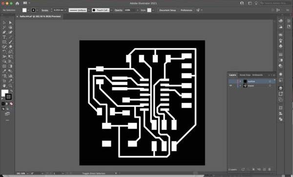
Next I exported this as svg with these settings:
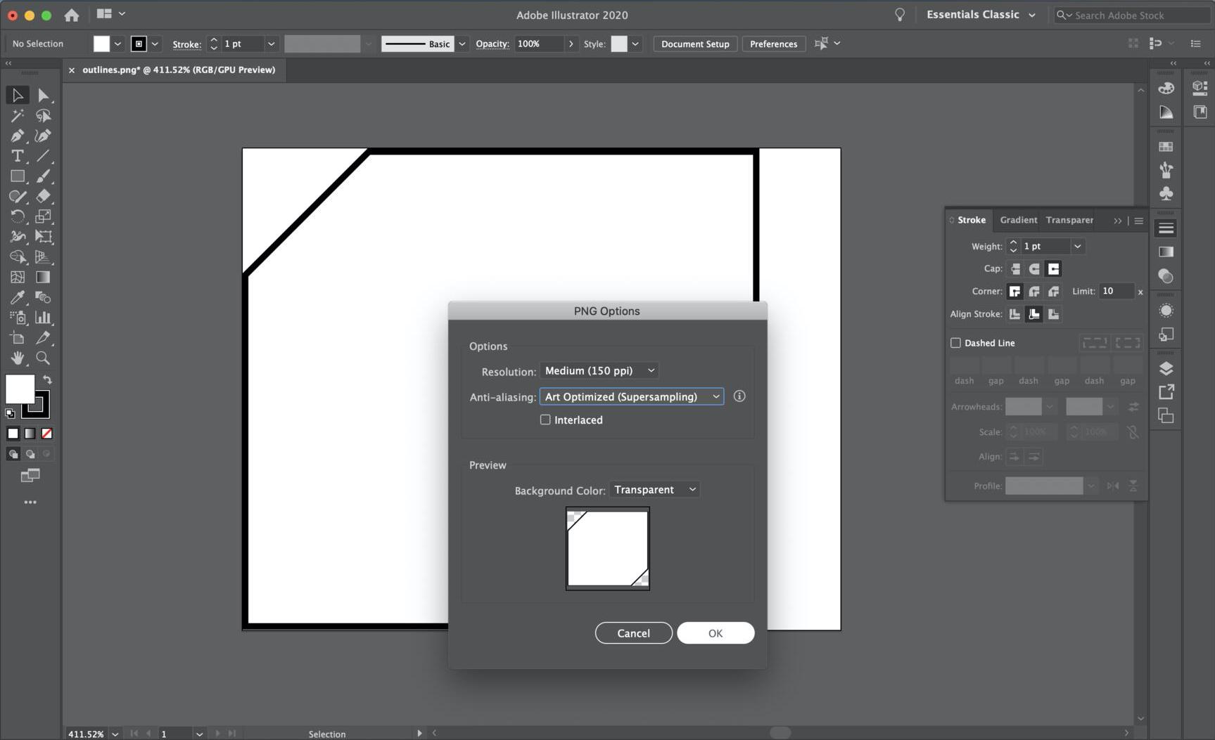
I opened the svg in Adobe Illustrator, made new layers for the traces and outline respectively.
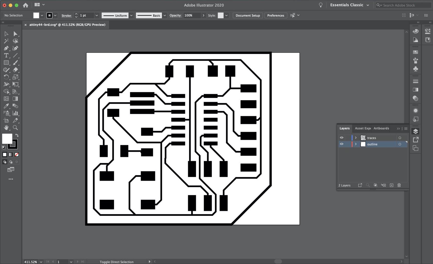
Then, after checking that the model is in mm, exported both layers separately at 150dpi in png.
Creating Toolpaths
I followed the same process as Electronics Production week to make toolpaths, mill the board, solder components and test the board.
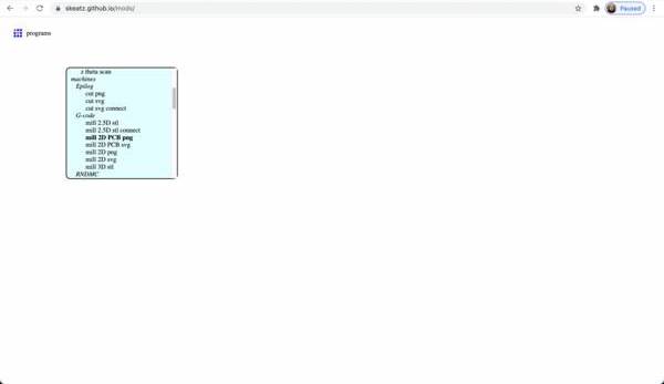
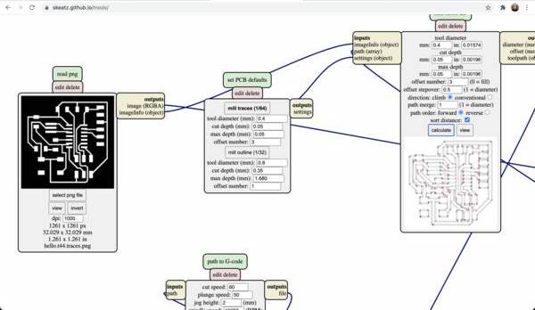
But this time I used Mods instead of Fabmodules. Here’s the process:
Designing in Eagle
I also tried to make the board in Eagle. The process was exactly similar:
-
Adding components in schematic:
-
Connecting and labelling:
-
In board, rearranging and making traces. Set trace width and grid size to 16:
-
Exporting is a little different from KiCAD. You need to keep all layers except traces and milling and then export dxf.
-
Open in adobe illustrator, set layers and export png in 1000dpi.
-
This time I used mods (local version created by Steven Chew) to generate nc files.
FabLab SP uses stepcraft machines that work with nc format.
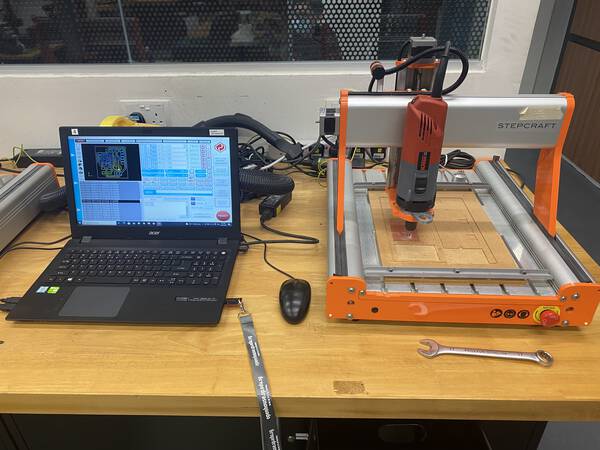
Milling and Stuffing
I started to mill the board, solder the components by following the workflow described in Electronics Production week.
On the first attempt, the I found that the edges of outline were too close to the traces, and they were fragile.
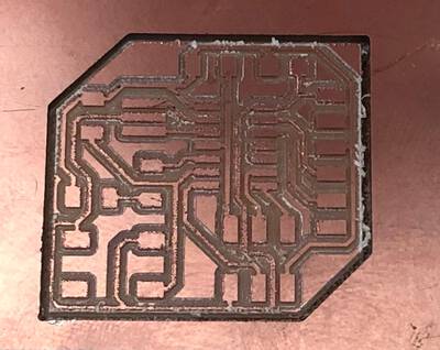
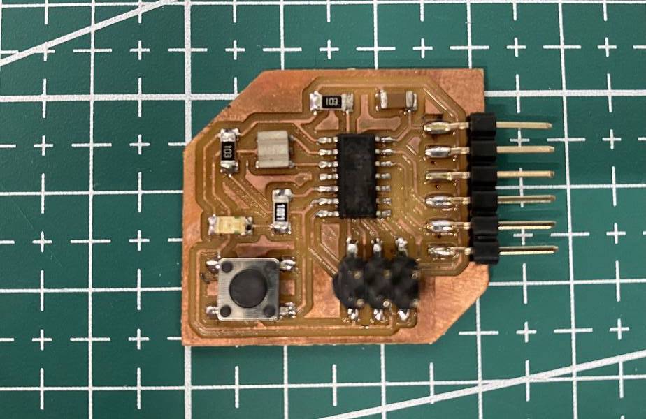
After offsetting the outline farther away, and milling the board again, I found that the pin headers were floating outside instead of resting on the board:
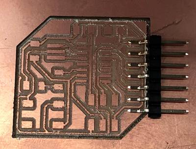
So chaning the outline accordingly, this is how the pins should rest:
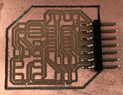
And after soldering all components, here is how the final board looks:
Programming and testing of the board is done during the Embedded Programming week.
3. References
Sparkfun KiCad beginners guide
Reference Documentation
4. Design Files
All design files in KiCad for SRM20 (rml)
All design files in Eagle for Stepcraft (nc)