7. Electronics Design
Group Assignment
To view the group assignment click here.
Individual Assignments
In this assignment I will redraw this hello-world board using “Eagle” software, , adding to it a button and LED and test it. After that, I will design the final project PCB using another software which is “EasyEDA”.

Redraw the PCB
To do this task I used “”EAGLE”, an electronic design automation (EDA) software, and I found it easy to use. Follow these steps to design the board after opening “Eagle”:
PCB components
- first, to add the library, Download the Component library. This is Fablab library, meaning that the components that are in the Fablab are present in it.
- Second , open “File” >> “new” >> “Schematic”, This window will appear. Click on “add part” icon to add a library or any component.
 To add library click “add part” >> “Open Library Manager” >> “Brows”.
 - Add these components that we will need to design the board:
- 10k ohm Resistor
- 1uF Capacitor
- ATtiny44 (UC_ATTINY44-SSU)
- J2 FTDI (CONN_06_FTDI-SMD-HEADER)
- ISP (CONN_03X2_AVRISPSMD)
- XTAL1 (XTAL_RESONATOR)
- button (SW_SWITCH_TACTILE_6MM)
- LED
Also add : - GND (Supply1 >> GND)
- VCC (Supply1 >> VCC)

- Link between the components using “Net” tool. Also use “Rotate”, “Move”, “Mirror” from the tool bar to help you in that.
- After you have finished linking, click “Generate/switch to board” at the left above the screen, to draw your PCB.

PCB connection
When you click “Generate/switch to board” this window will open.

- “Design Rule Check” are necessary, I knew their importance through my experiments in the fablab. For example when wanting to mill the PCB that we designed, and when the distance between the traces is less than the distance specified in the DRC, the milling machine may consider them as there is no distance between them and thus the milling is not done correctly. The three basic DRC checks is the width, spacing, and enclosure. So set your work through Design Rule Check (DRC) from “DRC” >> “Load” >> “open”.

- Connect between the components using “Route Airwire”, follow the fine yellow lines in connection because they are evidence of the connection between the components. ِِِAlso move the components in proportion to the connection.
NOTES:- When connecting XTAL1, there is no difference between connecting the two ends, but connecting the middle end correctly is the most important.
- Consider the direction of the LED.
- The board size can be controlled by pressing and moving the broad yellow line.

Problem1
To solve the problem of my inability to connect a path due to the conflict, I added a zero resistance, in order for this resistance to be the bridge on the opposing path.

Export the PCB
- Click on “Layee Settings” icon and “Hide Layers”.
- “Export” the file as an “Image”, choose “top” to export the traces and “dimension” to export the boarder.

- Choose “Monochrom” for the image to be black and white, so that the milling machine can recognize it. And choose “500” Resolution, the regular number for clarity of the image.

Result1


Problem2
Above the image appears an excess piece that increases the possibility of error, because it may not be milled properly, in addition to losing the material. To solve this problem download “GIMP” software and follow these steps:
- “Export” the board as an “Image” with both “top” layer and “dimension” layer.

- “open” the image in GIMP.
- Use “Crop to Content” to cut off the extra sides of the image.

- Use “Rectangle Select Tool” and “Paintbrush Tool”.
a. To get the border, cut the inside using “Rectangle Select Tool” and paint it black “Paintbrush Tool”.
b. For the traces, paint the white board in black using “Paintbrush Tool”.

Final Result


Milling the PCB
Using SRM-20; I refer to Electronics production week to recall the steps.
Problem
After completing the milling process, I found that the upper part of the left side is still connected and has not been milled at the appropriate depth as shown:

That is why I repeated the drilling process on the same piece but with more depth, but the result has not changed. I realize that the surface level is uneven, and the upper part was the lower level.

So I set the z-axis in relation to the depth of this upper left corner. The operation was successful!

Soldering
 NOTE: The direction of the LED must be observed, as the end of the green line is the end of the GND.
The Required Components

I soldered the components and I made sure that the connection is correct using the Multimeter. Everything was perfect!


Testing the PCB
Using Arduino
- I connected the FTDI cable into the my PCB to give it power. Then I connected it to a programmed PCB.

- Select your “Processor”, “Clock” and “Programmer”.

- To download the code that leads to the turn ON and OFF of the LED every second, go to “Files” >> “Examples” >> “Basics” >> “Blink”.
- “Upload Using Programmer” to upload the code.

- Here below shows that the PCB is functional.

Problem3
The first try testing my PCB, the light lasted for more than 10 seconds.
I “Burn Boatloader” and it’s work!

Files
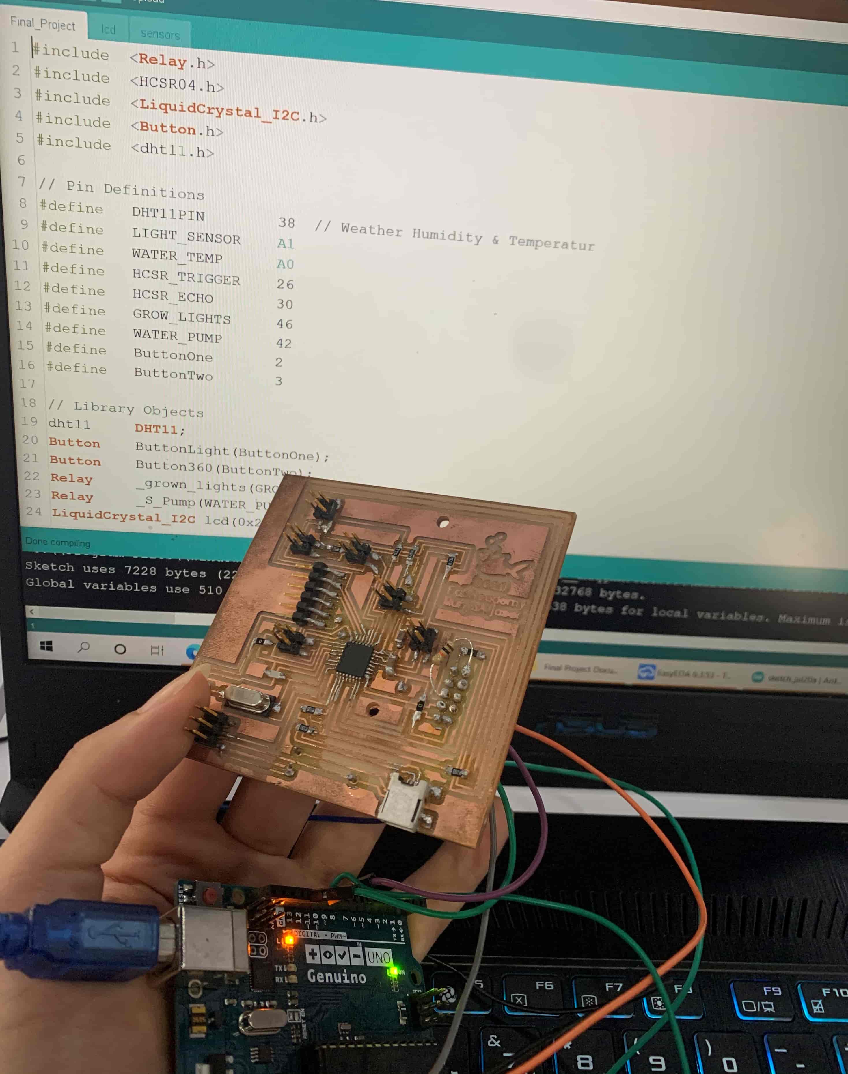
Designing PCB for my Final Project
The design of the Final Project circuit I used EasyEDA software, to download it click here. In the previous assignment, I used “Eagle”, in terms of designing there is no difference, but choosing the component, in this program EasyEDA has more options for choosing them.
I made three attempts to design the circuit, the first two were unsuccessful because of mistakes that I benefited from and I will avoid them happening next time.
The First Attempt
Problem 1
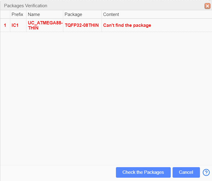
After I choose the components and I want to “Convert to PCB”; This window opens to me which says that “Can’t find the package” for my ATmega88.
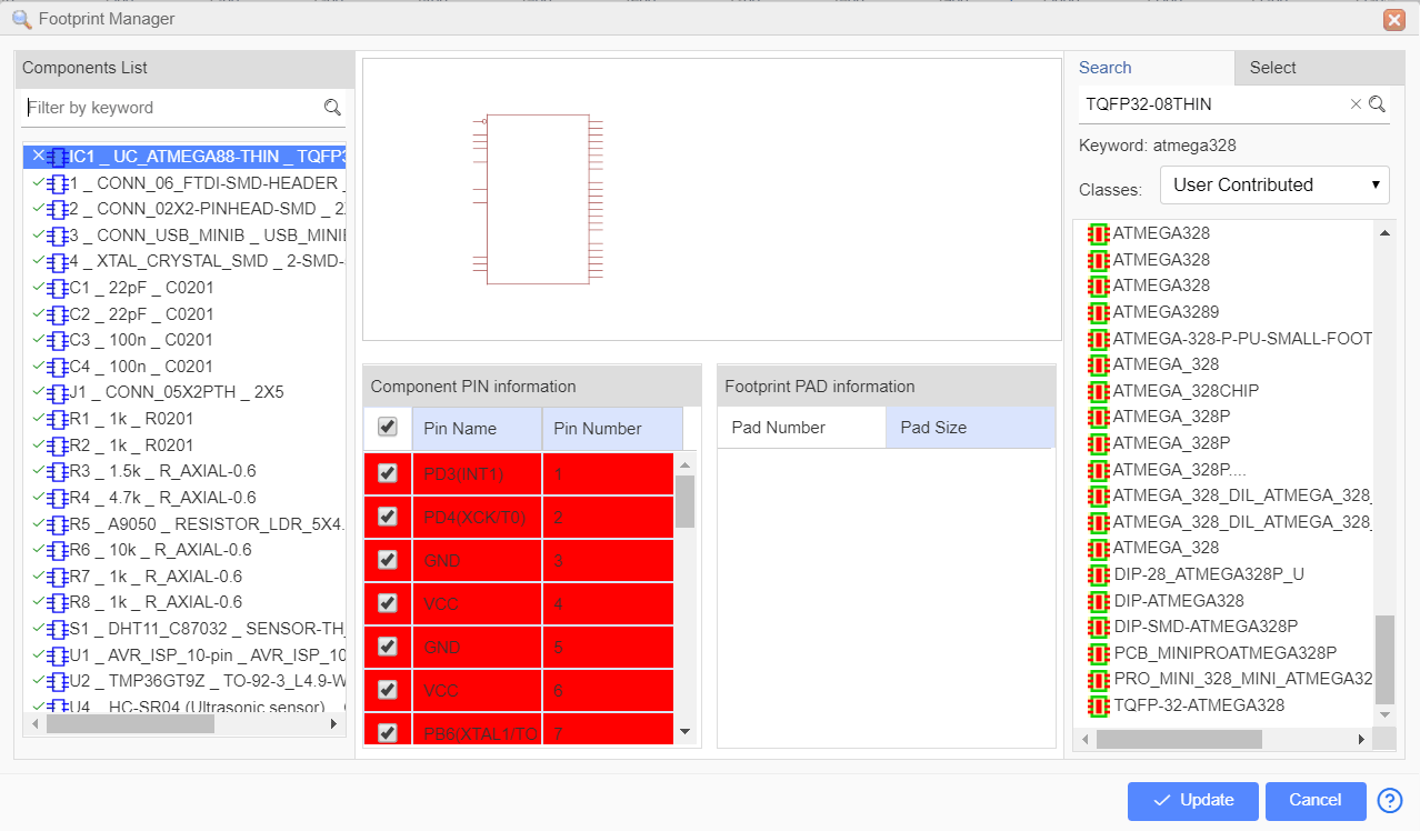
After I clicked on the “Check the Package” option in the previous window, this window appeared for me, which asked me to choose an alternative to my ATmega. I chose the first option, and then “Update”, but this didn’t solve the problem.
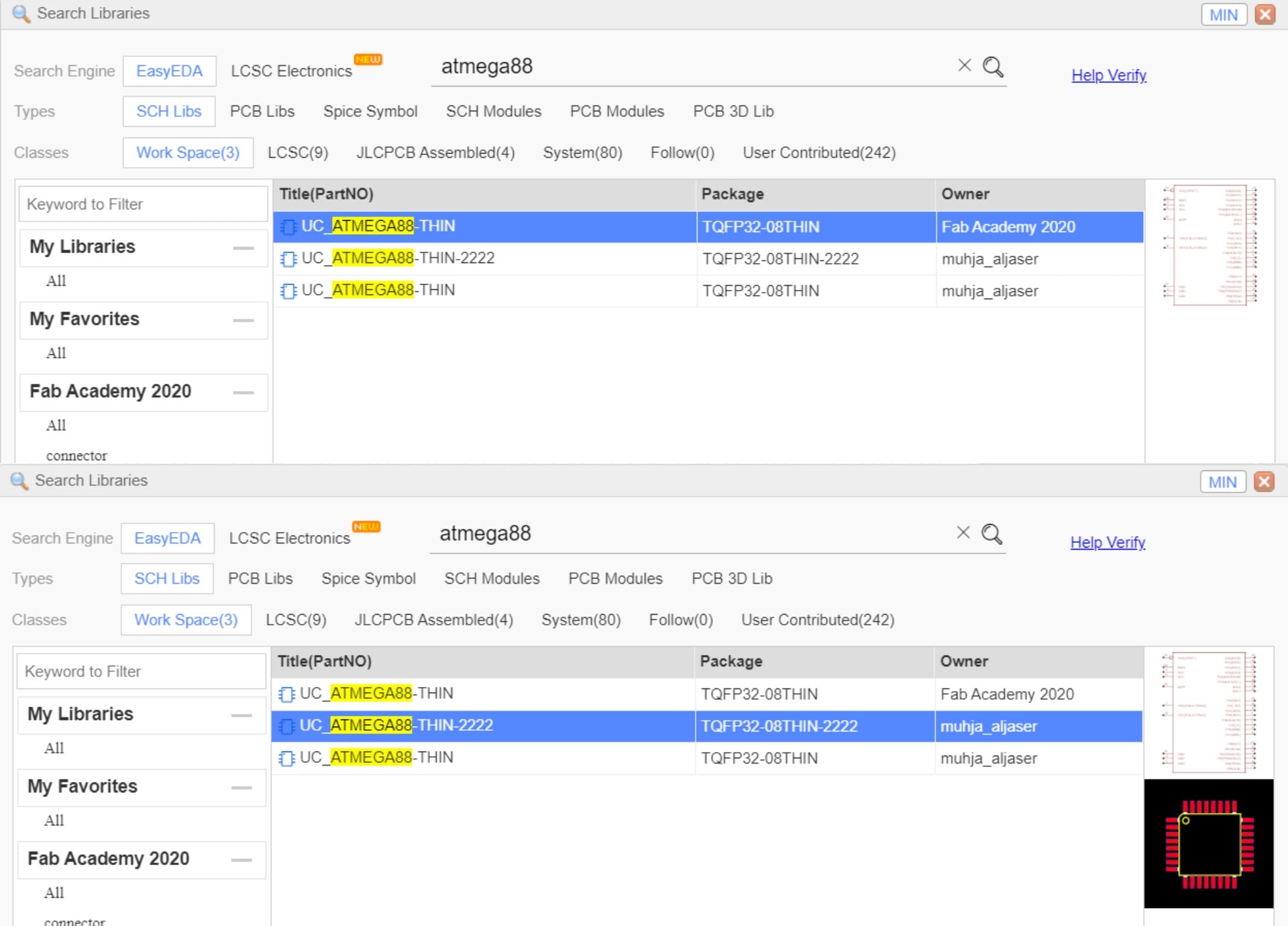
I added the same component from another library, with its image diagram, I exchange it from “UC_ARMEGA88 ThIN” to “UC_ARMEGA88 ThIN 2222” as I name it; The problem was solved. The problem was that the micro image did not exist.
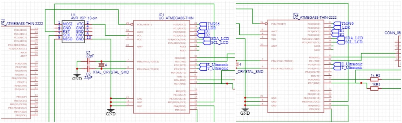
 I deleted the old micro and put the new micro in its place without changing the location of any part.
Problem 2
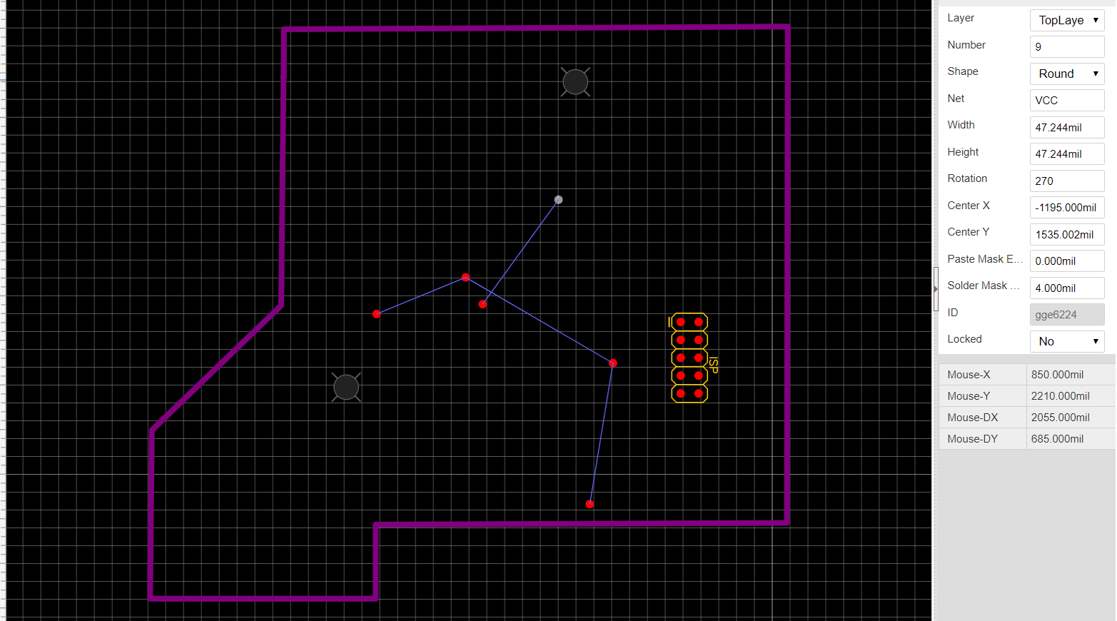
These are the “design rule” I used that I didn’t set it from the beginning of the design.
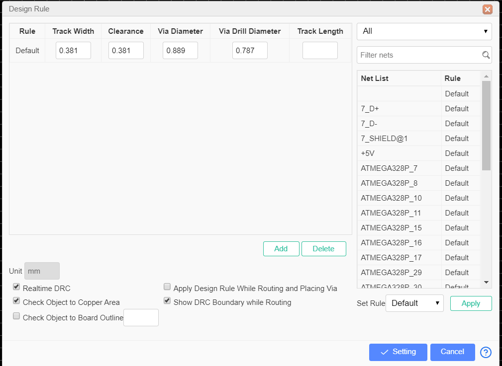
Resulting from design rule change, many ” DRC errors” can be checked by “Design Manager”. Appears in DCR errors “Track width” and “Clearance”. When you click on one of the errors it shows you the error location, which you have to adjust, after that click on the “Refresh arrow”, the number of the errors in the brackets decreases. You have to make this number zero. The “Track width” indicates that the width of the line is not equal to the width set in the design role.
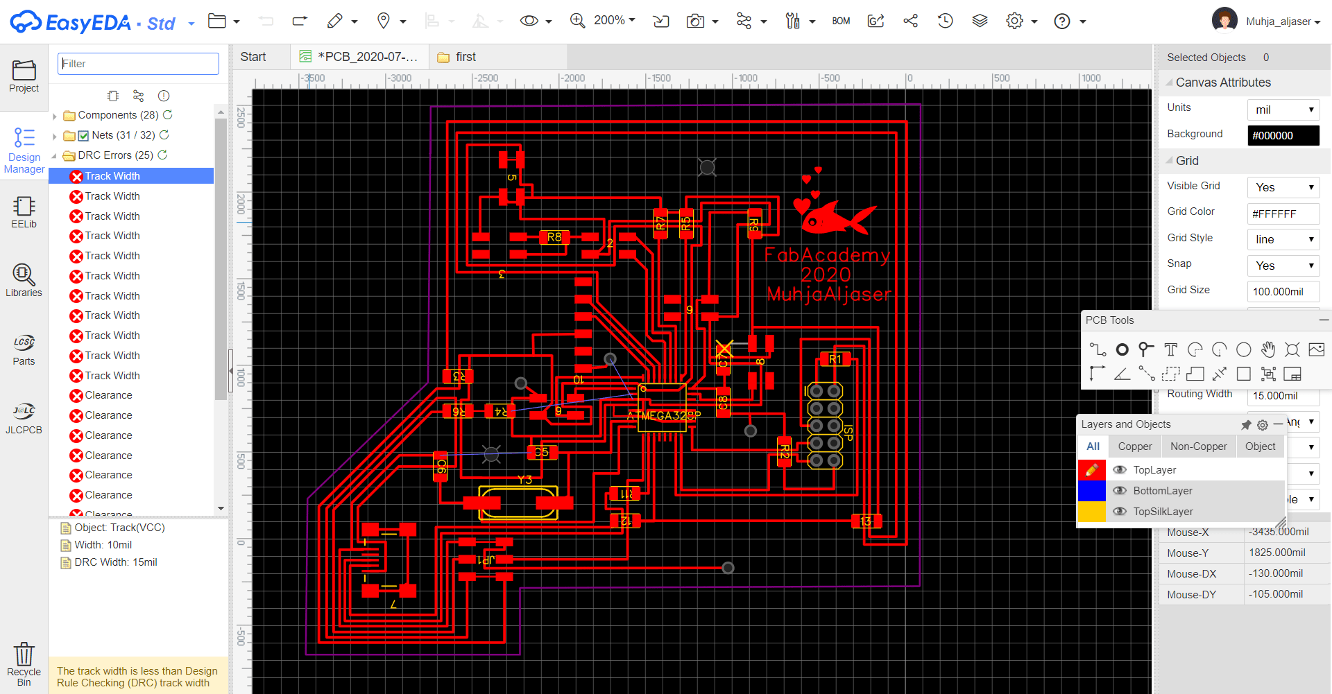 As for the Clarence, it indicates that there are traces that are close together; This can cause it not to be milled correctly.
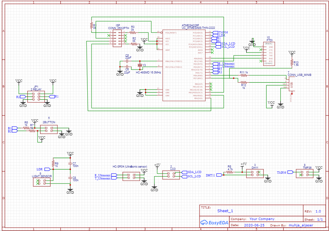
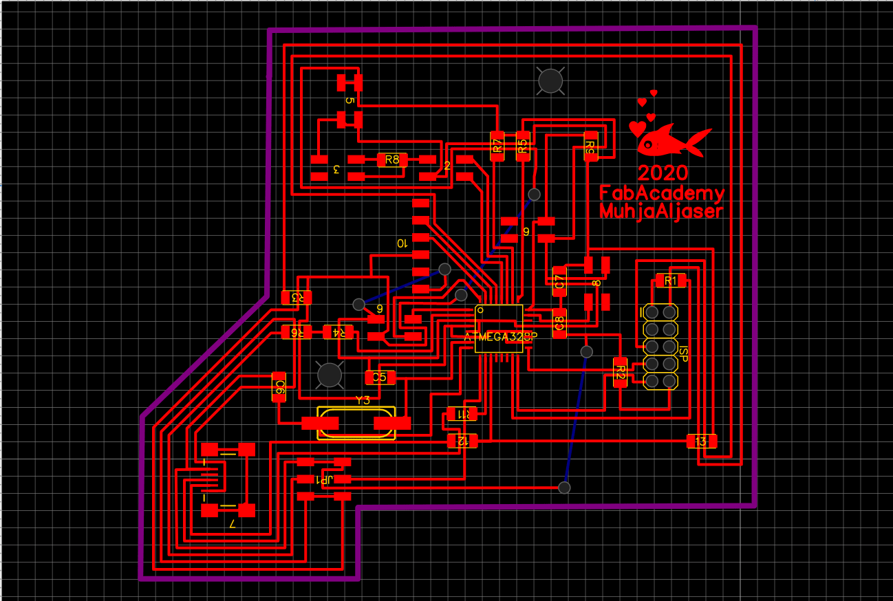
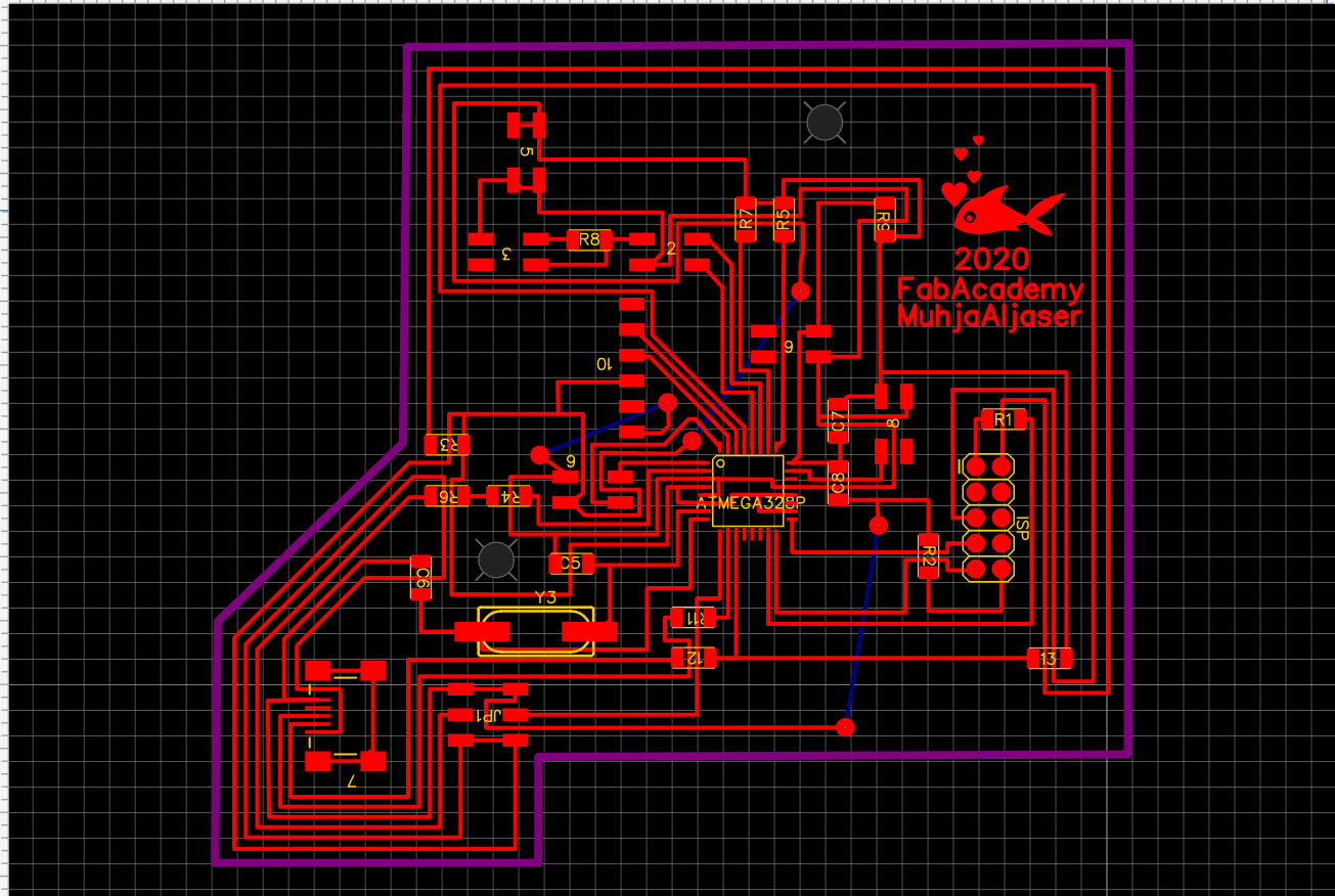
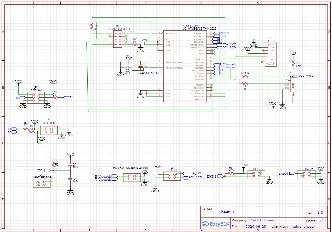
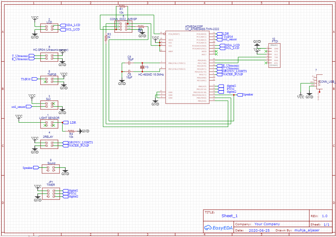
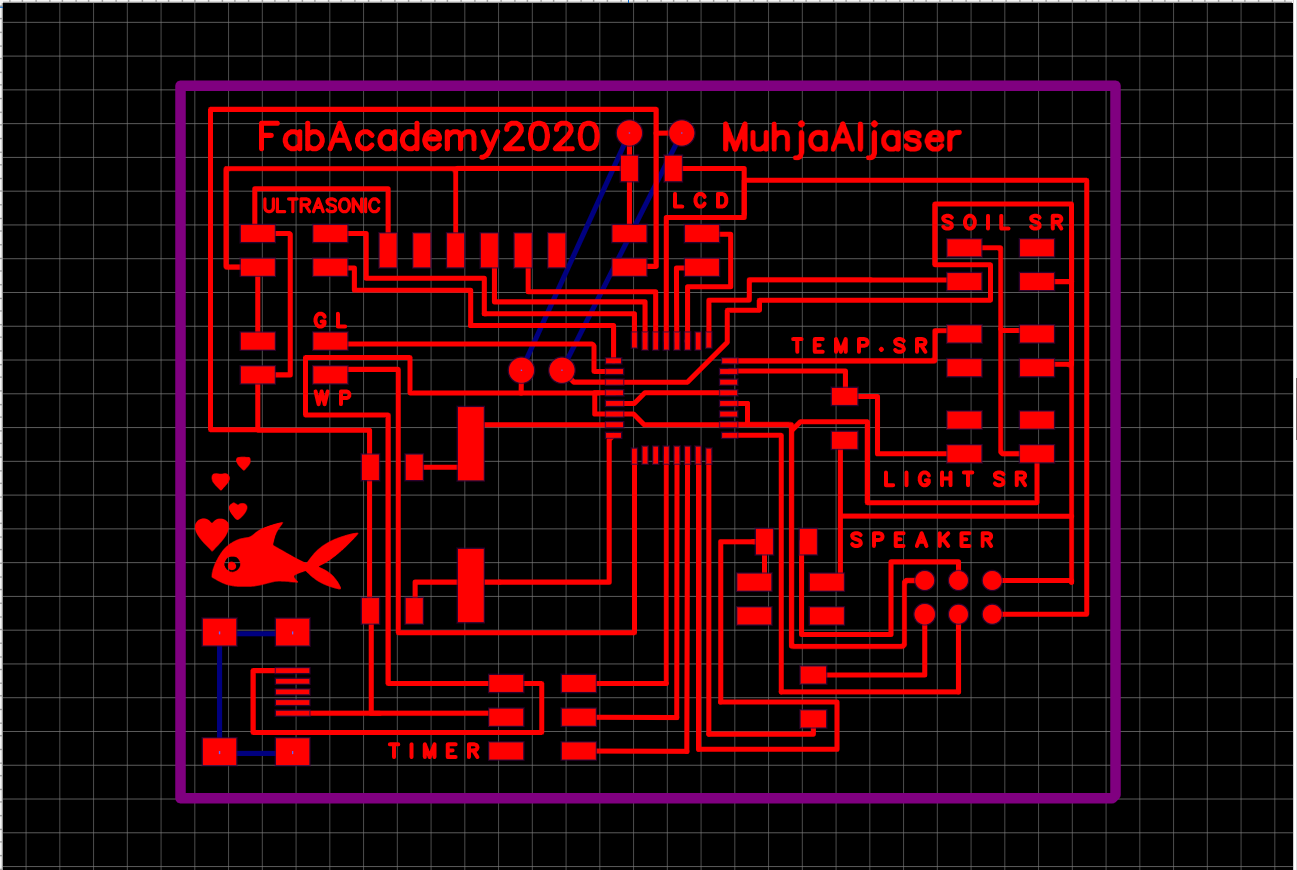
The Final PCB
These are two pictures of the PCB schematic and for the connection.
Exporting the PCB
The step before milling is to export the PCB.
- Top Layer > Convert the multi-layer holes to the top layer, and export it without Top silk layer)
 - Holes > Reduce the size of the holes, because this hole is the one that the machine will mill. I didn’t change the size of the holes in the previous step, in the “Top layer” just to facilitate soldering.
 - BoardOutLine > Do not mill the board outline before the milling the holes so that the PCB does not move when milling the holes.
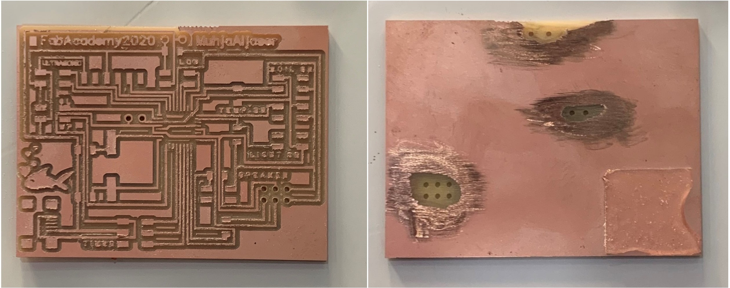
After Milling

Problem 4
After I used the multimeter to check the conductivity between the traces, I saw that the VCC is the same as the GND.
 The problem was that when I connected the wires behind the board I connected them to each other because the back layer is conductive as well. So I peeled off the position of the holes where the wire will be exposed. This was not the only problem causing.
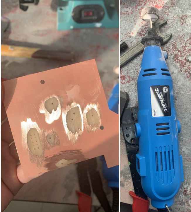 After being unable to find the problem in my soldering method, I followed the path of VCC and GND to see where they could meet, until I knew that the machine did not mill the board at a place where they were connected.
 I manually peeled this position to solve this problem.
Problem 5
This was the last problem I faced that I had to redesign the board, which is that when I wanted to solder the USB I realized that I had not positioned it correctly. Because when I want to plug the USB cable, I will not be able to do that, because the entrance will be on the inside of the board and not on the outside as I thought, where I will not be able due to the small space.
The Second Attempt
In my second attempt to design the board, I did not change anything except that I removed the jumper wires that I do not need and added what I need after putting the USB in its correct position.
This is how the board looked after the design was completed.
This is how after milling, I checked that no wires were not milled by the machine.
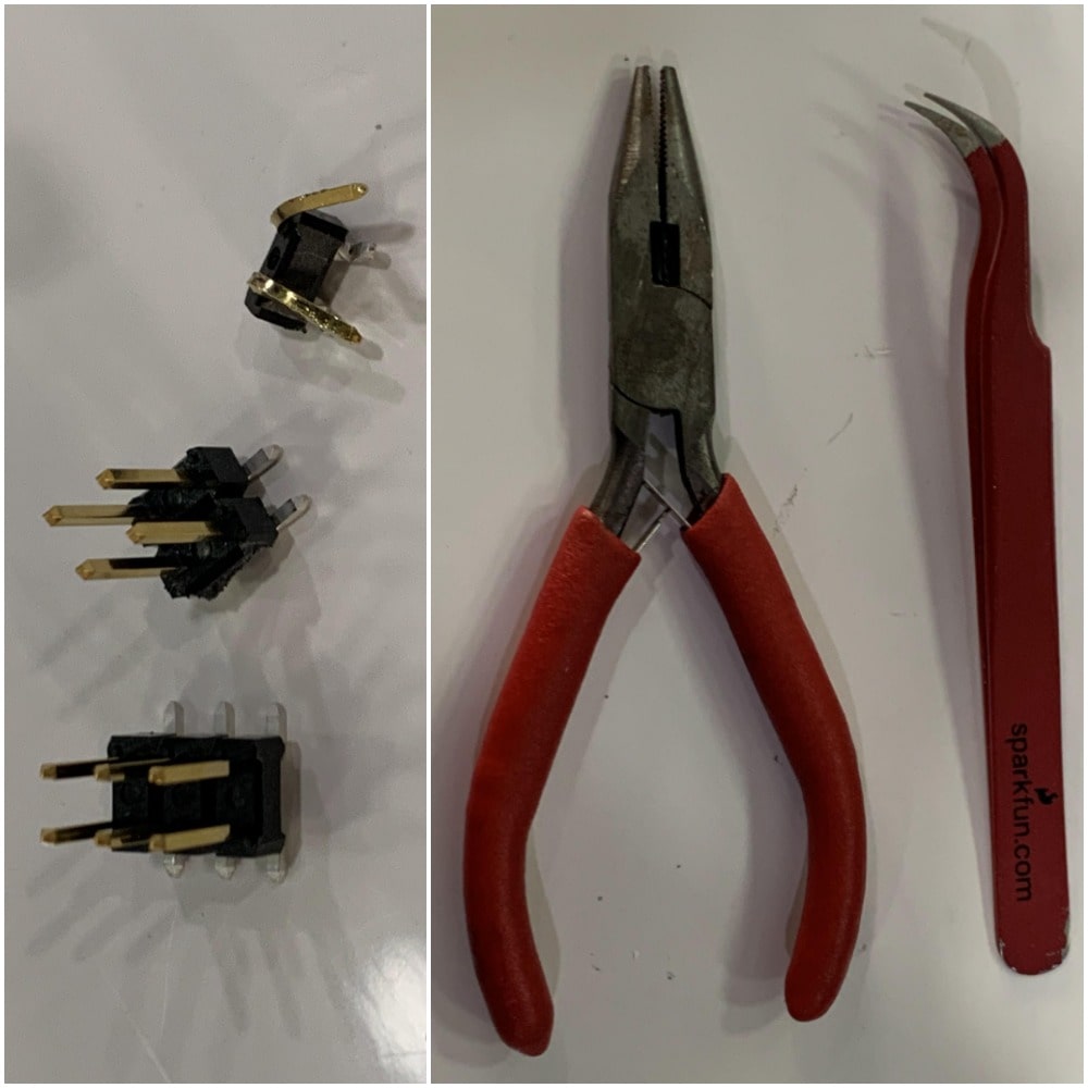
I did not have four headers, and the six headers could have been cut off.
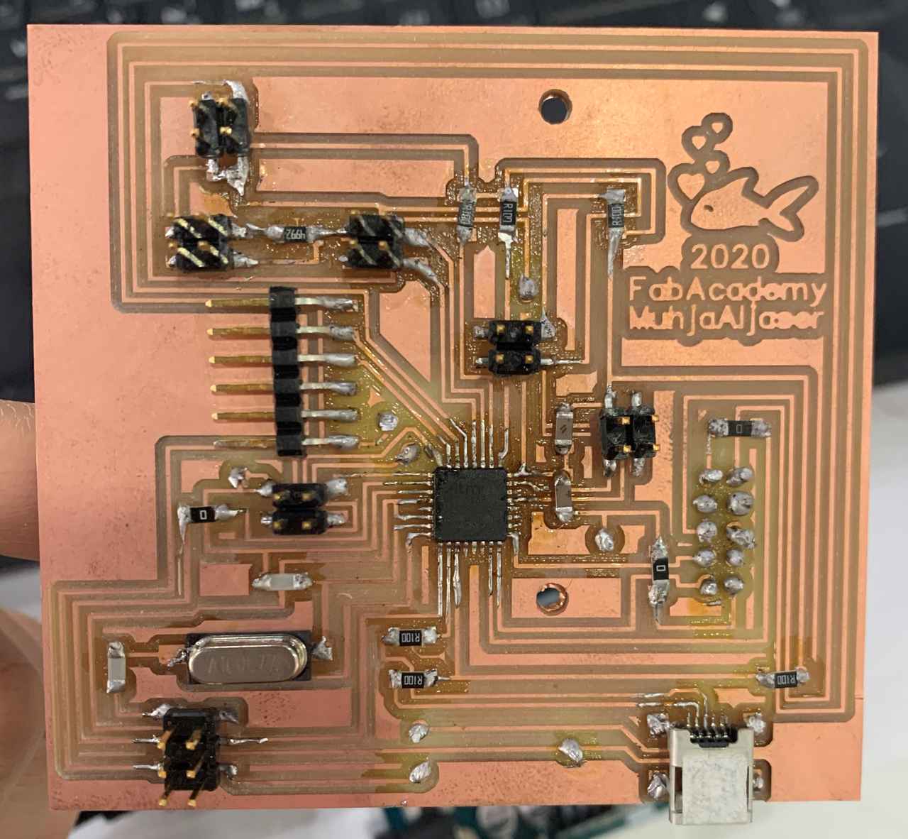
 This is how the board after I finished soldering.
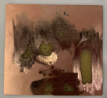
 The first thing I did after the milling was to peel the position of the holes from the back.
Programing
To set Arduino UNO in ISP mode, connect the Arduino UNO to the PC. Open Arduino IDE and open the ArduinoISP example file (File -> Examples -> ArduinoISP) and upload it.
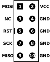
This is the ISP 10 headers top view.
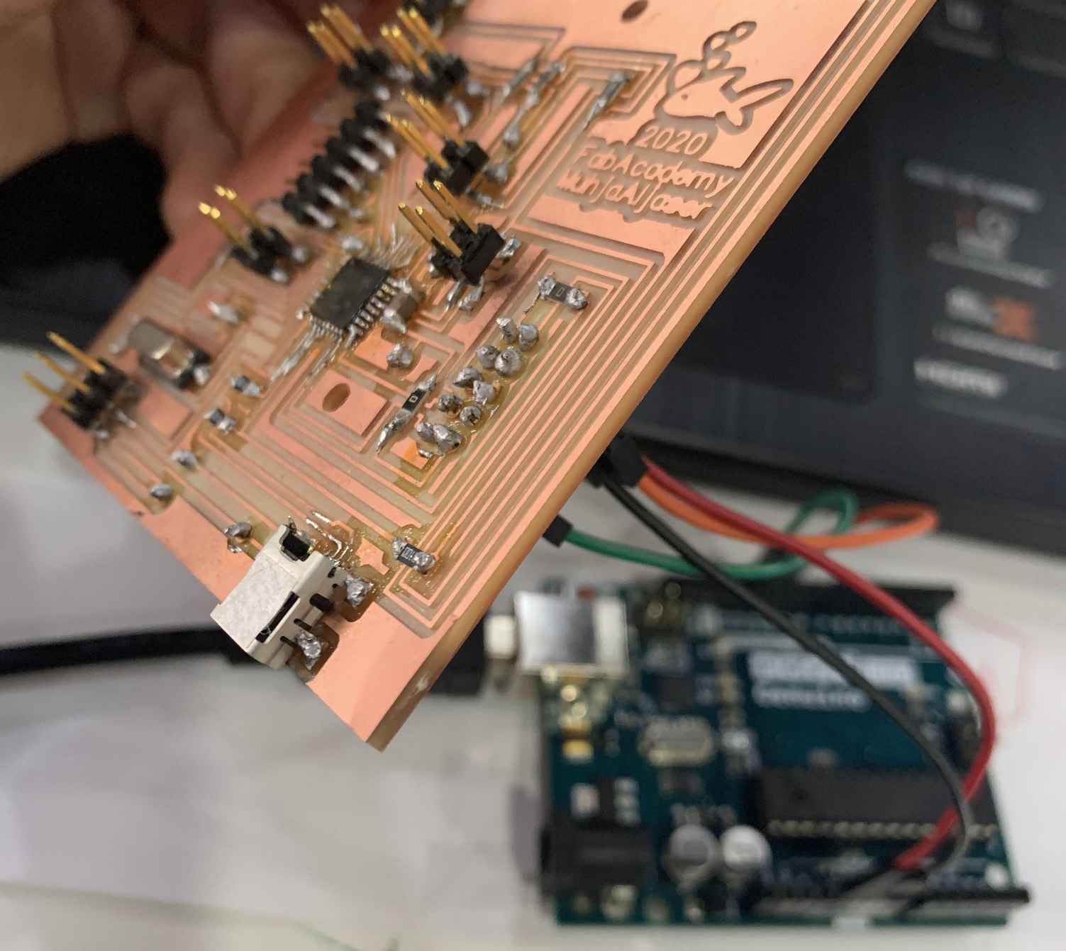
I connected the board ISP with Arduino UNO
UNO 5V –> VCC
UNO GND –> GND
UNO Pin 13 –> SCK
UNO Pin 12 –> MISO
UNO Pin 11 –> MOSI
UNO Pin 10 –> RESET
There is no result of this connection, no code can be uploaded on it.
Ptoblem 1
I realized that I have to put a resistor between VCC and the RESET in the ISP, so that not all the pins be RESET.
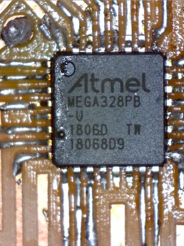
Problem 2
The main problem seemed to be that I soldered “ATmega328PB” instead of “ATmega328P”. Here I learned that the single letter makes a big difference in electronics.
This is the pinout for each of them, it seems that the difference is not great.
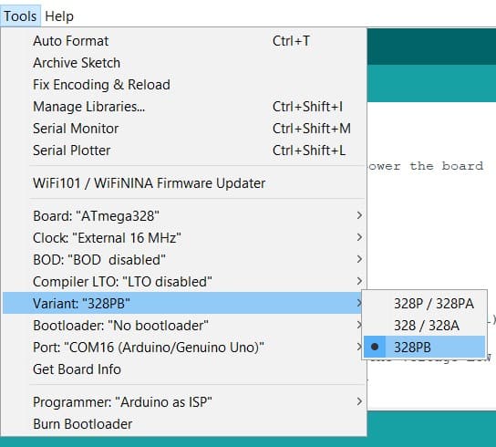
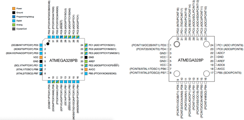 To start programming “ATmega328PB”, I followed the steps on MiniCore site, “How to install” >> “Boards Manager Installation”.
- Using Arduino IDE Open the “File” >> “Preferences” and enter the following URL in Additional Boards Manager URLs:
https://mcudude.github.io/MiniCore/package_MCUdude_MiniCore_index.json
- Open “Tools” >> “Board” >> “Boards Manager”. Search for “MiniCore” and install it.
- Make sure the latest version is installed for “Arduino AVR boards” from the “Boards Manager”.
Here I could compile the code on the board.
 To write the code correctly, I must know the Arduino pins for the microcontroller.
 I was putting every component and upload the code on it separately. Here it shows that the sound is interrupted when the distance measured by the ultrasonic is less than 7cm.
After that, I tried, again and again, to upload the code to the board but there was no result.

The Third and the Final Attempt
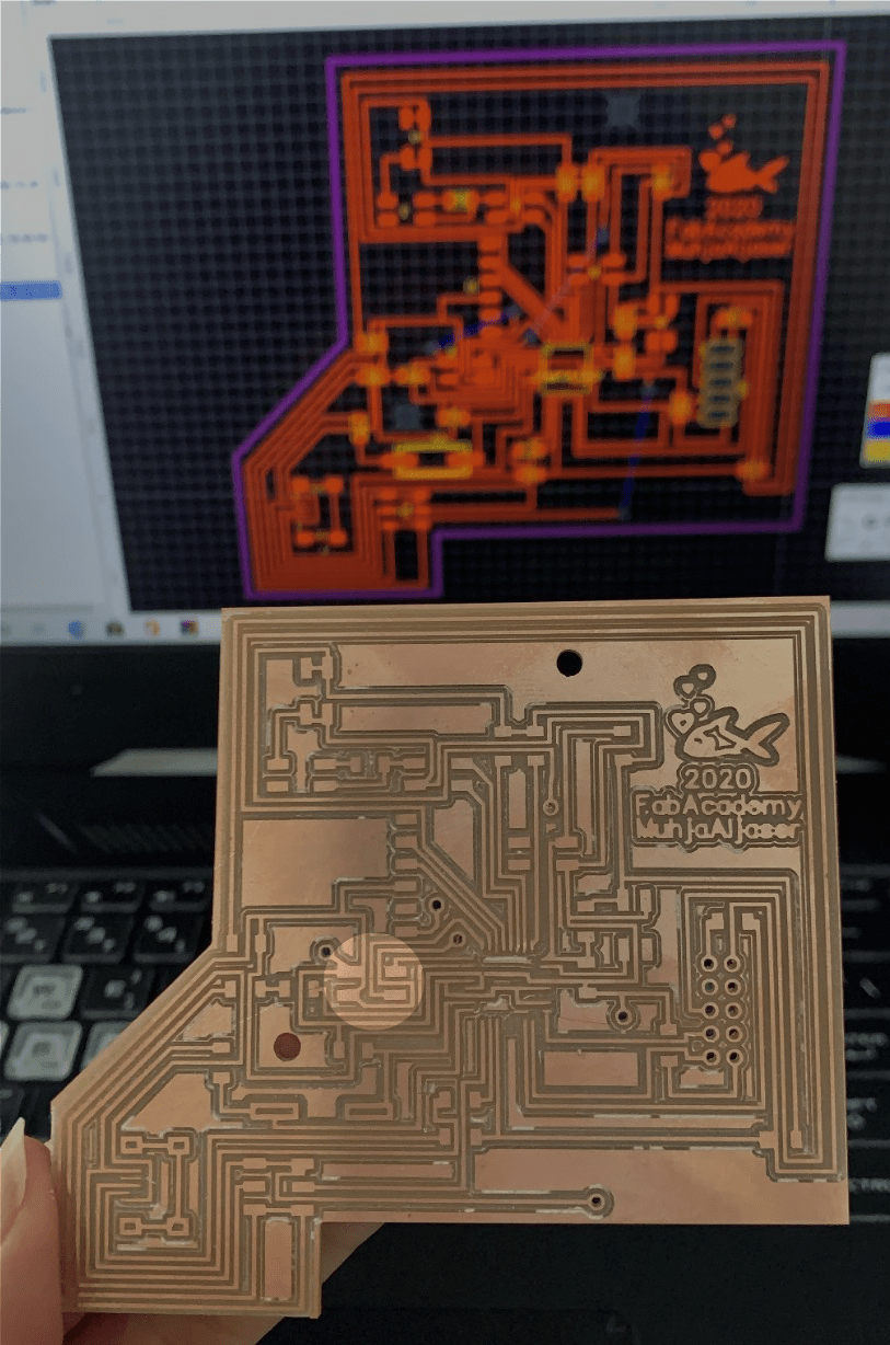
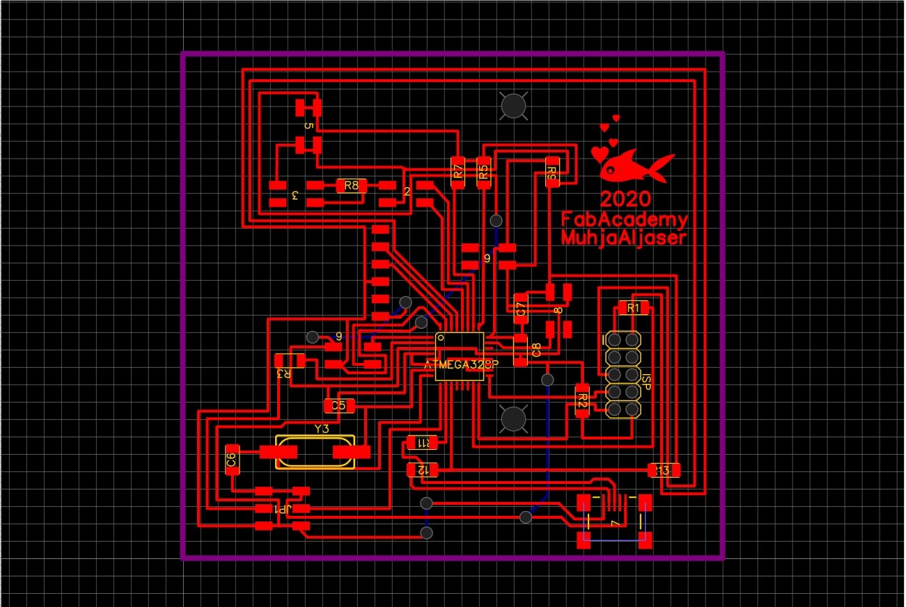
This is schematic and I made some adjustments to it by removing and adding some inputs and outputs headers.
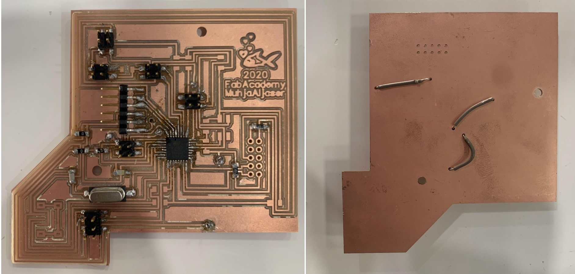
 This is how the PCB looks.
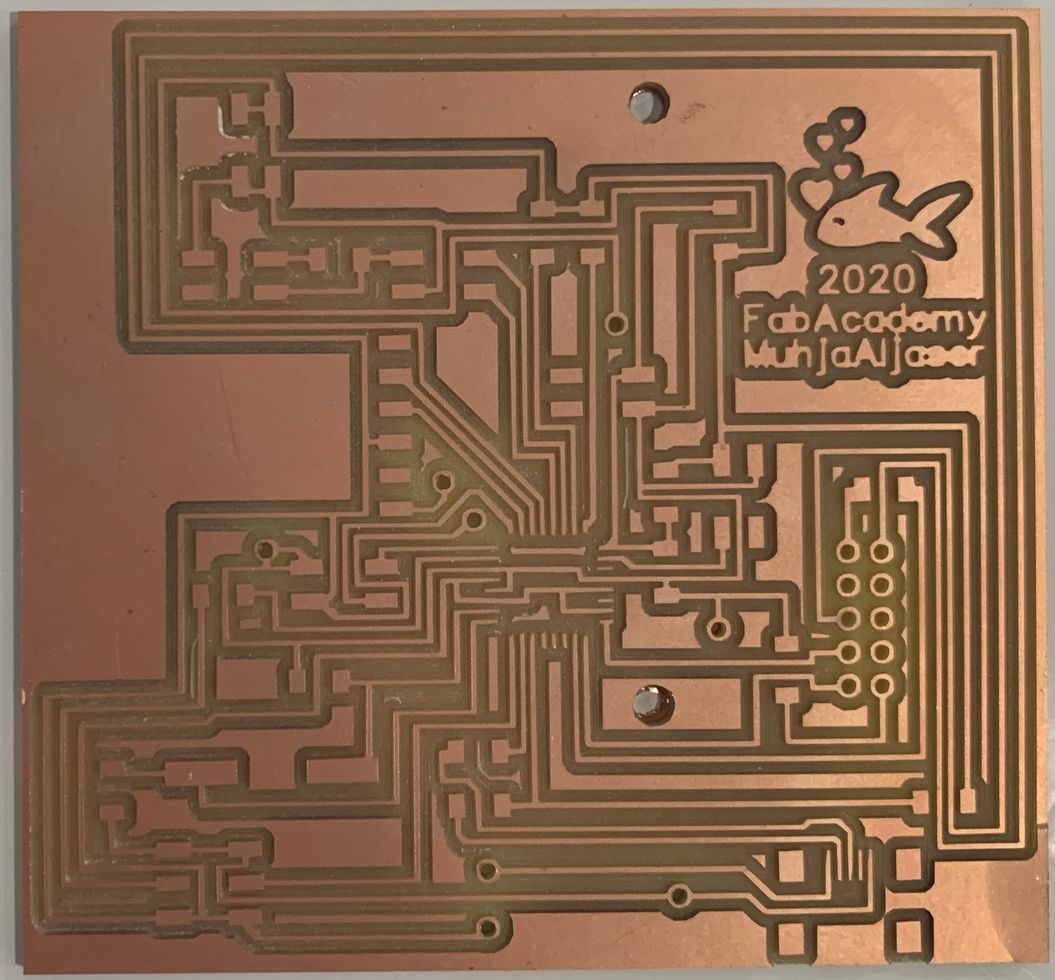
 This is how the PCB looks after milling. And of course, I don’t forget to peel off the back layer.
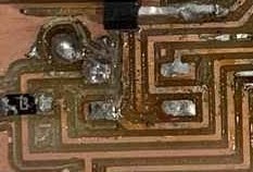
 Before I mill the holes on the board, I look at it to make sure if it needs to be milled again. There are two tracks the machine didn’t mill it, but no problem I will peel them manually. It became clear to me after that that I didn’t check the “Clearance” for them.
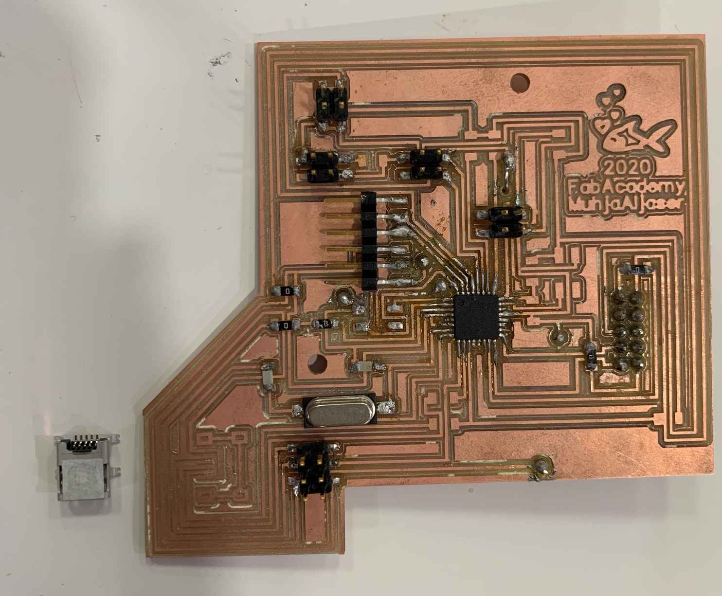
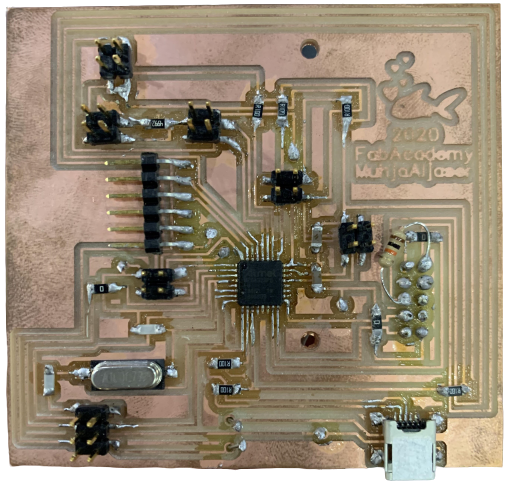
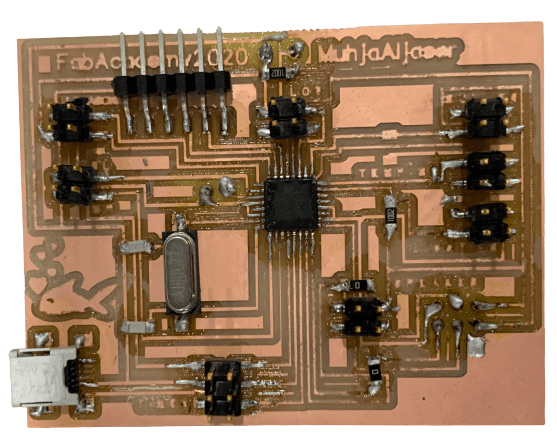
![]() This is how the PCB looks after solderig.
This is how the PCB looks after solderig.