Week 11
Input Devices
Link to the class content- Group assignment
Measure the analog levels and digital signals in an input device.
- Individual assignments
Measure something: add a sensor to a microcontroller board that you have designed and read it.
- Learning outcomes:
Demonstrate workflows used in circuit board design and fabrication. Implement and interpret programming protocols - Have you:
Described your design and fabrication process using words/images/screenshots or linked to previous examples. Explained the programming process/es you used and how the microcontroller datasheet helped you. Explained problems and how you fixed them. Included original design files and code.
Group assignment
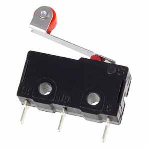
Limit switch Input device:
- Digital Signals:
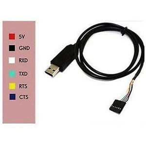
- Connect FTDI cable between the circuit board with the respective pins. (VCC-VCC)(GND-GND)(TX-RX)(RX-TX)
- Connect the limit switch. (COM-GND),(NO-VCC)
- To enable my PC read my board I did this tutorial.
- Open Arduino: tools - Port COM12 (in my case) - serial plotter.
- Analog levels:
- To know how to use the oscillator I watch this tutorial.
- Connect (VCC-VCC), (GND-GND).
Design
Final project
Sketch Plan
We made a sketch plan with the help of our instructor about the in-put and out-put devices that our final projects will need. We discus about what is the most important characteristic of our projects, in my case the principal characteristic is that the shelter open and close. For the input devices I gonna need the next items:
- Solar panel: give energy to the circuit board.
- Limit switch: determine the position of the shelter.
- Bluetooth: communicate between the circuit board located in one side and the second one at the other side.
- Charge module: is about to charge the battery.
- Battery: save the energy collected by the solar panel.
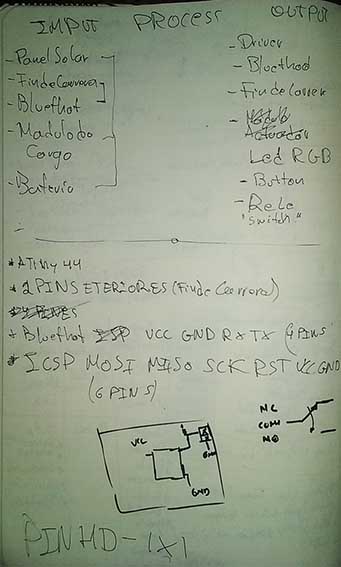
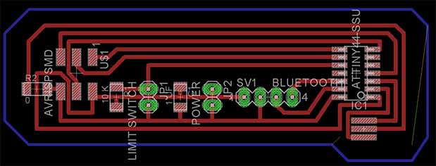
Components:
- 1 X ATTINy 44
- 1 X PIN HEADER-1X2 (Limit switch)
- 1 X PIN HEADER-1X2 (Power supply)
- 1 X 10K RESISTOR
- 1 X PIN HEADER MA04-1 (Bluetooth)
- 1 X AVRISPSMD 2X03SMD
- 1 X 1UF Capacitor
- 1 X Resonator
- 1 X 0 Ohm resistor
Eagle
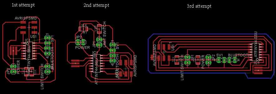
I started creating a new project and opening the schematic window after that I added the components and organize them. It was a little difficult at the bigging to think how the connections gonna be but after some attempts and fixing some errors I managed to create the connections of all components.
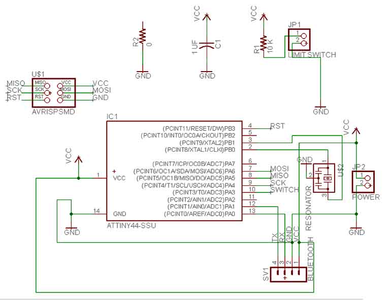
With the schematic ready I change to the board view and started to organize my components. This part was more difficult than the last one, I did it tree times until I complete the objective at the 3rd attempt.
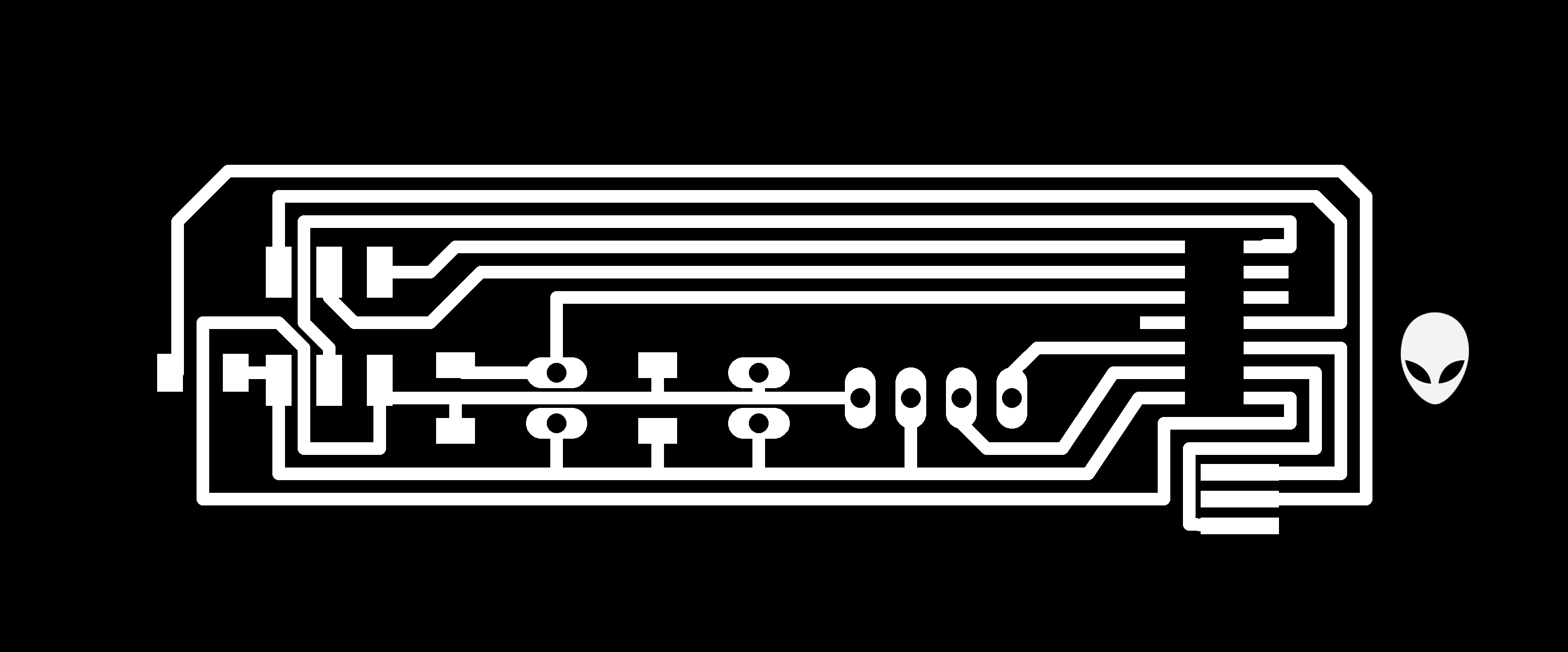
PNG Error
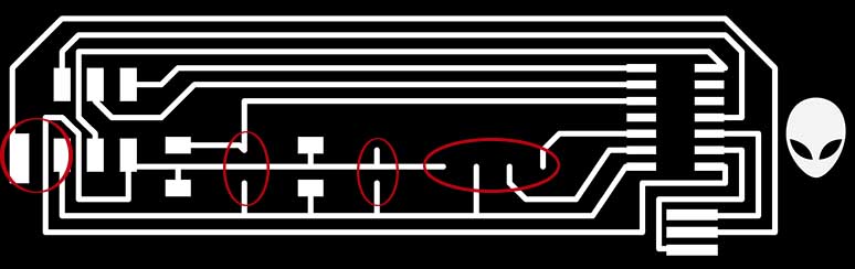
Finally export the file to png following the same work flow I did the for the week07, at that moment I didn't realized that I turn off the "pads" layer and because of that I had some troubles. Additional to that error I realized that my VCC connection for the Capacitor wasn't connected for that I create a bridge between the VCC Pin of the AVRISP, that don't look to good but I debug that after.
After that I use Photoshop to edit my PNG file adding an alien face.
Mods Error
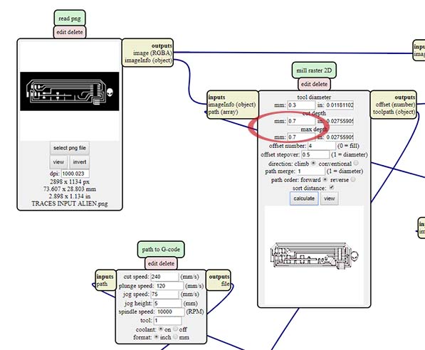
I didn't listen well the recommendation from Alex about the parameters and I put in the tool depth 0.7 instead of 0.07 that causes me some problems.
Machining error
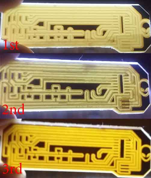
With my G-code ready I open it in LinuxCNC software to mill my PCB. I machine tree times the PCB:
- 1st attempt: The tool that I used for the milling of the traces was a 30 degrees mulling cutter and for the cut 60 degrees. Because of I set up the cut depth to 0.7 instead of 0.07 the milling cutter low too much and ate all the traces.
- 2nd attempt: I didn't realized yet about what happed and I started to suspect that maybe something with the cut dept was wrong or maybe I was wrong and put the tools one instead of the other. So I just change the the milling cutter 60 degrees for the milling of the traces and the 30 degrees tool for the cut and the result was bad again the traces were to small.
- 3rd attempt: This time I change the configurations in mods for the cut depth to 0.4 and the result was acceptable but not the best.
Soldering Error
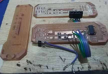
At this moment I realized that my circuit board was wrong because the traces were to small and the pads of the pins wasn't there because I forgot to turn on the pads layer in eagle when I create the PNG file.
Despite of the errors I try to solder the pins using cables but the traces were too small and I burn them in the attempt. And that was the moment that I decided to create a new circuit board taking into account all the errors that I had.
Debugging
Eagle
For the design of the board this time I add a resistor of 0 ohms
- In the schematic file I add a 0 Ohm resistor.
- In the board file I increase the size of the rout from 0.016 to 0.024.
- In the board file I join the VCC connection between the Resonator and the AVRISPSMD using the 0 Ohms resistor as a bridge.
- And this time I didn't forget to turn on the pads layer when I export the file to PNG.
You can download the files:
I use Photoshop one more time to edit my PNG file adding an alien face.
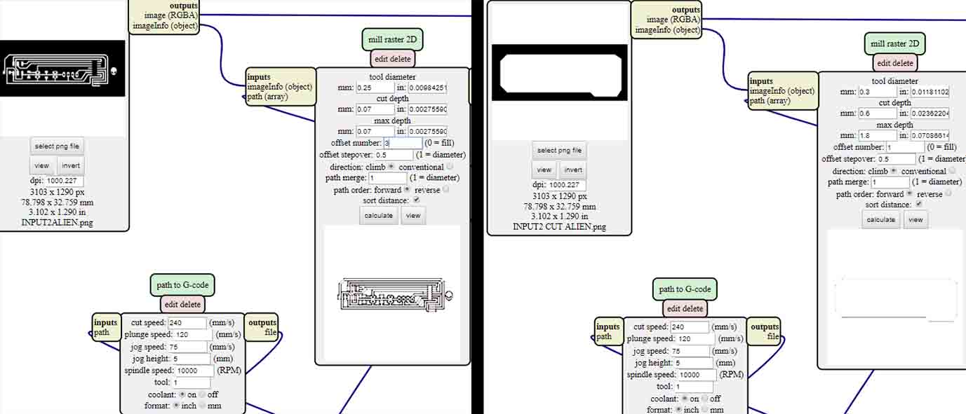
Mods
Traces:
- Diameter tool: 0.25
- Cut depth: 0.07
- Max cut depth: 0.07
- Offset number: 3
Cut:
- Diameter tool: 0.3
- Cut depth: 0.6
- Max cut depth: 1.8
You can download the files:
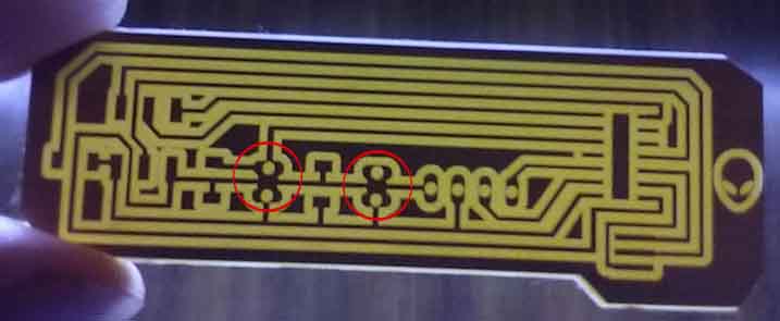
Machining
This time the PCB result very well just with a little error in the pads of the pins for the limit switch and the pins for power supply. In Mods I didn't realized that in those parts the space between the pads and the traces was too close and because of that the settings of the tool diameter of 0.25 didn't allow the milling cutter to pass in those parts.
Milling cutter: 30 degrees for the traces and 60 degrees for the cut.
To debug that I use a scalpel to separate the pads from the traces.
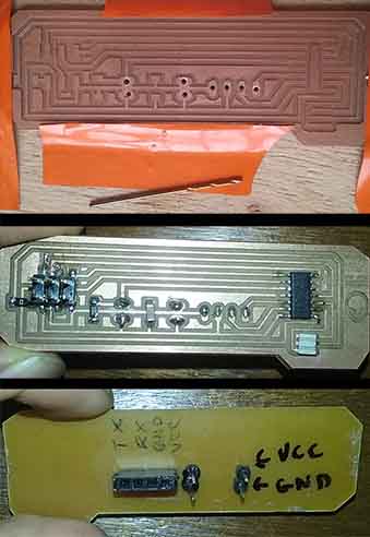
Holes
To make the holes in the PCB I use a tiny drill bit. Because this was the first time I do this and at the bigging I think to make the holes was a little difficult but it was really easy even though I broke the tiny drill bit because I put to much strength.
Soldering
This time soldering the components was easier than before but very laborious specially the micro controller.
Programing
Arduino Software
Open the digital serial and Software serial examples:
Copy the software serial to digital serial and specify "mySerial" to the correspondent baud "9600" and the delay "100".
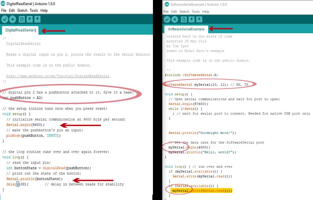
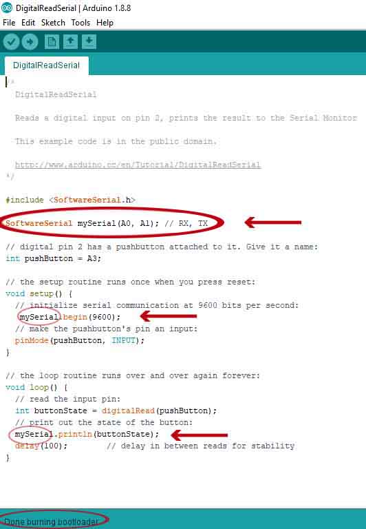
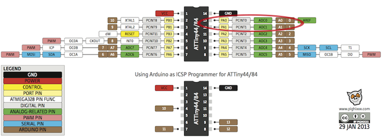
Specify the RX and TX pins attached to the board also the pin attached to the switch, for that I had to review the schematic of my board and compare with the ATtiny 44 arduino pin-out.
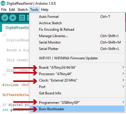
The next step is Burn Bootloader:
- Board: ATtiny44
- Processor: ATtiny44
- Clock: External 20 MHz
- Programer: USBtinyISP
- Burn Bootloader
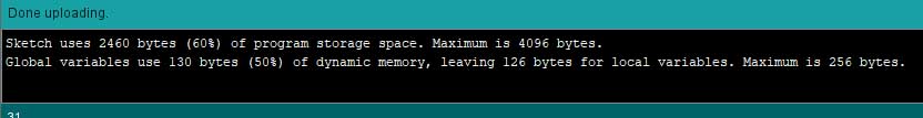
And finally Upload!
You can download the file:
Hello world
I programed my Input board with the "hello-wold C-code" For that I followed the step described in the week 09 and this time I have to set up my C-code to fit my Attiny 44 micro controller.
hello.ftdi.44.echo.c:
- F_CPU 20000000UL
- serial_port PORTA
- serial_direction DDRA
- serial_pins PINA
- serial_pin_in (1 << PA0)
- serial_pin_out (1 << PA1)
make:
- F_CPU = 20000000
- MMCU = attiny44
- t44
You can download the file: