11 - Input Devices
Sensing The World
Tools & Assignment
 Updated for 2019 evaluation standards!
Group assignment
Updated for 2019 evaluation standards!
Group assignment
- Probe an input device’s analog levels and digital signals
Individual assignment
- Measure something: add a sensor to a microcontroller board that you have designed and read it.
Learning outcomes
- Demonstrate workflows used in circuit board design and fabrication
- Implement and interpret programming protocols
Have you?
- Described your design and fabrication process using words/images/screenshots or linked to previous examples.
- Explained the programming process/es you used and how the microcontroller datasheet helped you.
- Explained problems and how you fixed them
- Included original design files and code
FAQ
Q: Is the satsha kit/fabduino I fabricated considered a valid board for this assignment?
A: Fabricating an unmodified board is considered as electronics production. It doesn’t count towards any design skill. You must make some significant changes to the original satsha kit/fabduino, for the board to be considered your own design.
(Copy of my 2016 website, with spelling corrections :)
Preamble
From the start of the Fab Academy I was interested in using FPGA / PSoC in my project.
So I decided I was going to use it for this project; I had never used it before.
Sensor of Choice
I decided to use a PSoC as a microcontroller, and I used the possibility of creating a Step Response sensor as a witty way around designing a really simple board (while sticking to the rules)
Step Response as Proximity Sensor
A step response sensor is essentially a copper plate that, in combination with the users hand, becomes a “capacitor”.
This functionality allows for different types of responses by altering the basic functionalities of capacitors by, for example, distancing your hand. In my case I will use step response to make a proximity sensor.
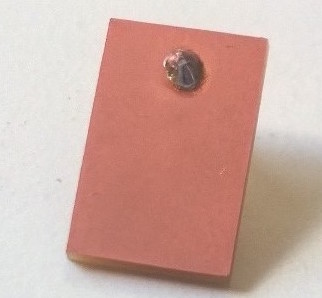
The board
The PSoC allows for an internal reconfiguration of components. This meant I could design 99% of the board internally.
However, since we had to make a board, the board I made was probability the simplest board possible (this compensates for how complicated it is to use a PSoC). Practically just a copper board.
Step Response board
Due to the small surface area of this small board it’s capabilities as a proximity sensor aren’t really that great, it’s more like a touch sensor really. Using a ruler, as seen in the image gallery actually works much better.
The PSoC
PSoC is a board with a programmable architecture.
Cypress has for sale a very cheap kit, which in combination with the Cypress IDE PSoC Creator (3.3) makes programming the PSoC “Easy” (and when I say easy I mean a little less close to Hell™ then the other methods).
Okay, it wasn’t THAT bad… I actually didn’t have many problems or issues, the biggest issue was how daunting the IDE, and the programming, was.
Even if it was basic C language, the API is generated automatically, this means that a whole lot of commands and projects which needed to be included are generated only after you build the project, which is confusing.
PSoC’s aren’t common, so there isn’t a lot of community support.
This means a very small amount of external documentation, which often is outdated.
Fortunately the guys at Cypress do an amazing job at documentation, but the huge amount of pages makes it hard to go through in one week.
Installing
Steps
1. Ordering the part (which Emma did from Farnell).
2. Subscribing to the Cypress website.
3. Installing a software which is required to download from the Cypress site.
After which
I could finally download Cypress PSoC creator 3.3, this only works on Windows (The install process is also very long).
Installing is quite tedious there are three different .exe programs to download, and the choice is amongst at least 9 downloads specific for the PSoC 4 CY8CKIT-049 4xxx of which I am using the PSoC 4 CY8CKIT-049 42xx PSoC.
Amongst the PSoC 4 M-series about 30 possible downloads (which I had to scavenge through to find example projects)…
Also, I had to Update to 3.3 from 3.1…
This was crucial and solved a lot of problems that I couldn’t figure out…
Programming
The first thing I did was look at the tutorials on the Cypress site. Programming was not necessarily difficult but very complicated, using the right commands depended a lot on what configuration used, since the API is generated rather then being a downloaded standard.
This meant that without reading the documentation, it was impossible to do anything, it also makes it prone to errors.
I started by using the SCB_BootableBlinking example which changed the speed at which the intermittent LED’s on the PSoC blink.
Bootloading
There is a very specific procedure to upload a program to the PSoC.
First you need to hold down the button on the board to make sure that it’s in bootable mode when you plug it in.
The second thing that needs to be done is that after building, it’s necessary that its programmed to the board using the bootable.
The third thing was finding the file and building a file with a bootable module, without it the Cortex0 folder which should contain the bootable file needed to control the PSoC.
This means that the bulk of the example projects CAN’T be used because this is the cheap kit (4€ versus 10€) we can’t program it directly but instead we need to…
Never Finished This Page
This is as far as the original documentation takes me, I added a Downloads header but added no link, & I can’t recall my way around the files I have locally.
Meaning we can see the results of my work but have no explanation of how they work or how to use them, meaning this work is practically worthless.
Meaning week will need re-doing, it’s a real shame because I had worked quite hard on programming the PSoC as I recall.
Additionally it could have been an interesting addition to the FAB Academy documentation, since not many people use PSoC’s.
Some images of the results are below.
Gallery
No Contact
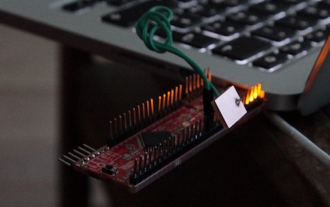
Finger not close to pad -> Proximity sensor off
Contact
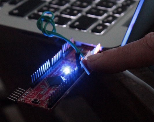
Finger close to pad -> Proximity sensor on
More Range
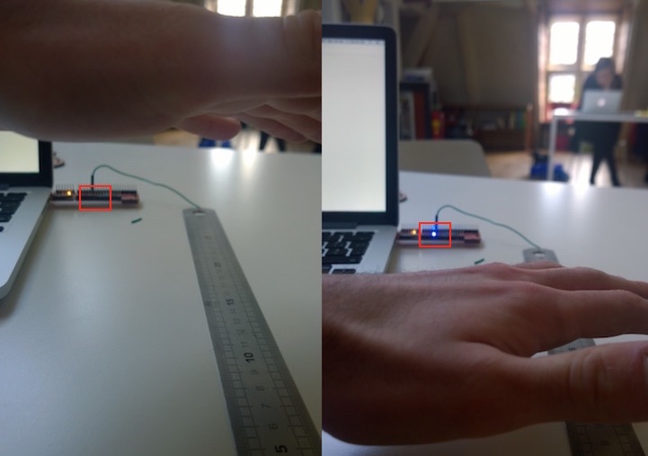
Step Response using cutting edge sensor technology [ie. a ruler]
2019
HexaPawn has a basic user interface, similar to a chess board or tic-tac-toe.
On a 3 by 3 board the player (white) has to make a move with one of his pawns, this can either be one square forwards or one square diagonally, to capture an opponent.
Our interactive board will need a way to record the moves which have been made.
This is obviously proximity / touch input, and we have a few ways to go about it.
We could use an infrared proximity sensor, which would suffice for detecting which of the board squares a pawn had moved too.
At that point, if we need a touch sensor, we might as well skimp on money by avoiding the *insert sarcastic tone* hugely expensive IR sensors and instead using step/capacitive sensors.
This will also add continuity from my work in 2016.
We can guarantee that a movement is unique in each case by ‘lift to placement’ combos.
What I mean by that is, every time we move a pawn from A to B, we get a lifting response at A and a placing one at B, if we record both, we can ensure uniqueness of moves, as well as finding illegal moves.
To note, with this method, pawns don’t have unique identifiers, so it can be played with anything that triggers the sensors.
In contrast to, for example, if I created “smart pawns” which used RFID, which should be possible according to this blog post, but is too much of a hassle.
Now the question is, how do we go about creating a step-response sensor.
Background Research
First things first lets find who has done something like this in the past.
I start my search from the obvious place, the ‘step response’ section of the Input Devices week.
Here we find two interesting links:
-> Matt Blackshaw - Week 8: Input Devices -Touchpad
->Matt Keeter - Capacitive Multitouch
Both these guys have an array of capacitive sensors.
Two things to note:
- These guys cover a small, but detailed, surface area
- They want stand alone, I want something that I can use for the networking week :)
They both seem highly inspired by Neil’s step-response board, fair enough.
I stumbled across this as well when I searched ‘step response sensor attiny’ on google:
-> Adam Harris - 2014: Input Devices
He has this redesigned version of Neil’s board connected to a cool looking antenna
My approach
As I pointed out in the notes I made above, the surface areas of the above examples are somewhat small.
Additionally they aren’t very serviceable, if a single pad is damaged the whole lot is to throw.
When the surface area is tiny that’s fine, but in my case it be best to have interchangeable plates.
This may seem like a dumb problem to address, but having witnessed what skin oil from handling and 3 years can do to a fabISP (aka break it) it’s actually a concern for me.
Protecting Bare PCBs
Copper will naturally oxidise and erode over time, particularly if there are traces of oils from your hands when handling the board.
There are a few ways we can protect the boards from this:
The first obvious choice is using a PCB mask, but it’s too much of a bother to deal with it.
The second is to coating the PCB with plain old nail polish, like seen here, which can also make the PCB waterproof-ish (all 3 methods shown in the video would work too, but the last two are overkill).
It’s not clear, however, how nail polish will react with bare copper, I’ve done my trails and nothing broke so far, but I remain skeptical.
I need 9 points of resolution (3x3), we could connect each pad up to an IO pin, that would take 9 digital IO pins.
Alternatively using multiplexing to address the pads in (row, column) combinations.
That would take up 6 digital IO pins, I’m not sure if 3 extra pins are vital, but there is no need to waste pins.
In either case, the attiny45 is too small, so it’s going to have to be the attiny44.
Originally I thought a single AVR with multiplexing would be the best way forwards.
However, with further inspection, it’s fairly hard to get this right.
Blackshaw does it by overlapping copper cut-outs made with the vinyl cutter, and his pads are cut diagonally.
Keeter does it with through whole connections and 0 Ohms resistors, and uses diodes to prevent leaking of capacitance.
Keeter’s solution is great, but afraid it will require some dark magic to get it work (aka it’s beyond my knowledge).
What I will do instead, is that each pad will share a send pin, and each pad will have it’s own output pin.
This consume a total of 10 IO pins which leaves us with a 2 free IO pins!
Fortunately we only need 1 pin for FTDI communication (sending), and for programing the board we can share the programming pins.
Sensor Pad - Design
The copper pad/plates which will act as sensors are more aesthetics then electronics.
Not sure if there is an easy way to design this kind of design in KiCad, but I will do in in Inkscape, since that will be faster then me learning how to do so.
Pad Design
I’m well aware that because we’re dealing with copper, we can’t really have the ‘black/white’ as we do with a normal chess board.
However we can etch some interesting pattern to make a distinction.
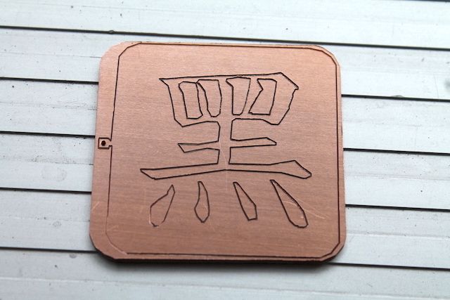
My choice for is 黒 - kuro, the Japanese character for ‘black’.
Here is how it will look.
Color - Inkscape
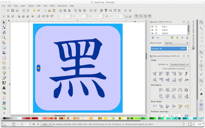
Traces - Black

Traces - White

Cutout

The size of the pad is 1.75 inches, about 4.5 cm which is the standard size for chess squares.
I know these design dimensions through Inkscape, and they are 1:1 with fabmodules.
The holes in the design are 1/32 inches which I round up to 0.035 in because thats the size of the cut-out bit plus as small offset.
Let’s cut one out and see how it will look.
Design Mistake
In my original design, the solder pad has a glaring fault, it’s detached from the main copper body!
By the time I realized I had milled out most copper pads and re-cutting everything would have been a waste, since it can be fixed with some solder.
The inkscape file corrects this mistake, the images above show what I used.
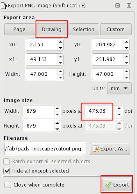
Inkscape Export Settings
A very import note to make, after several failed attempts at trying to drill small holes, I discovered that hte DPI of image you give to the fab modules actually matters.
From testing 475 dpi is a good number.
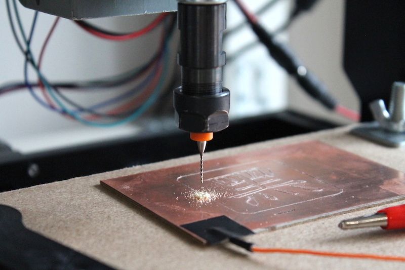
Sensor Pad - Cutting
First thing do do is get the .gcode files using the fab modules, in this case we can just load the .png files we just exported from Inkscape.
Using Mods Mantra
Positive is to keep. Negative is to remove.
The settings used for the mods follow from week 5.
Traces
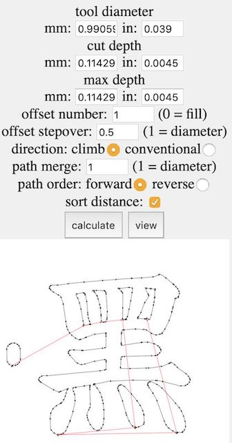
Cutout
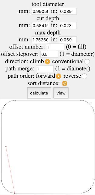
Yes here I’m using the 1mm milling bit for both jobs.
This doesn’t match the 0.8mm hole, or the typical trace dimensions.
I don’t really care for detail on these, just fast production.
Then we can go to our trusted 3018 &bCNC combo to get the pads cut out.
This isn’t actually the final design of the pads, but a prototype, as can be seen by the connected, and squared, pad.
The photo below was my favourite though, you’ll see me use this sensor in this tutorial (didn’t want to ruin the nice ones for testing), while the above design and milling settings are for the final versions of the pads, which will go in the final project.
In the image it might appear that the lower left side of the edge of the board, and the character, are not fully milled out, in fact, the light coloration is caused by some left over pcb material, which I wasn’t able to remove with the use of soap, if you zoom into the picture you will clearly see the step near the edge of the cut.
This material was later removed using a precision knife very easily, but a second photo was not taken.
Un-milled traces on my particular PCB look dark and shiny.
Use An AVR & Make It Sense Capacitance
To make things nice and easy our first step is get our knowledge up to speed.
Q1 What AVR to use?
A1 We established in my approach that I will use theattiny44
Q2 Can the input pins be digital, or must they be analog?
The fastest way to answer the last question is to look at example code.
Q3 This begs the question, how will we do the programming?
A3 Neil offers a c code for this task, but I think I’ll go down the easy path this time around.
A simple google search “Capacitive sensor Arduino” will yield 1,830,000 results, the first of which, for me, is: Capacitive Sensing Library
This is our starting point, we got to read through that before we can go ahead.
Important notes made during read:
100 kilohm - 50 megohmresistor between the send pin and the sensor pin.- For many applications, a more useful range of values is obtained if the sensor is covered with paper, plastic, or another insulating material, so that users do not actually touch the metal foil.
- A small capacitor (
100 pF) or so from sensor pin to ground improves stability and repeatability. - A small capacitor (
20-400 pF) in parallel with the body capacitance, is highly desirable too, as it stabilizes the sensed readings. - Grounding: run a foil ground plane under the sensor foil (insulated by plastic, paper, etc.), and connected by a wire to ground. This worked really well to stabilize sensor values and also seemed to dramatically increase sensor sensitivity.
Guidelines:
- 1 megohm resistor (or less maybe) for absolute touch to activate.
- If the sensor is exposed metal, it is possible that the send pin will never be able to force a change in the receive (sensor) pin, and the sensor will timeout.
- Also experiment with small capacitors (
100 pF-.01 uF) to ground, on the sense pin. They improve stability of the sensor.
A2 There is nothing in the documentation or the example programs suggest digital pins are a problem.
Cool Demo Video : CapacitiveSensor Arduino Library, Demo on Teensy 2.0
This board should be fairly straight forward.
PCB Design in KiCad
I’ve never tried KiCad at this point, but Eagle is distant enough in my past to justify trying a different tool.
Using the rough sketch found on the arduino documentation, we create the following board design:

Here we can see the set of required 1M resistors between the sender pin and sensor pins, as well as the suggested100pF capacitors between the sensor pin and GND.
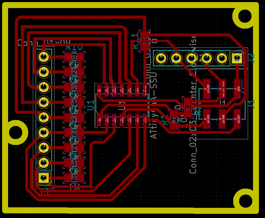
When it came to routing, I had to give up on the capacitors because routing had become impossible.
Did I try for many hours? Yes.
Could I have done it had I been a better PCB designer? Maybe.
In practice this will mean “less stable sensors”, not sure what that exactly entails, I guess we will find out (or hopefully not!).
One aspect to note about my PCB design is the use of 0805 components (capacitors and resistors),
which aren’t part of the FabAcademy inventory, but where the only one I could get an assortment of.
The inventory standard is 1206, which is a little larger.
The only difference between the two is difficulty in soldering and thermals, neither of these should prove to be an issue though.
When we export the design files for millings, usually it picks up things like holes in the THT components.
Since the output files are .svg, I normally open them in Inkscape to see if there are any unwanted artifacts, such as these.
Milling
We can load the svg file into the mods, and connect the svg component (detaching the png one).
Setting as follows:
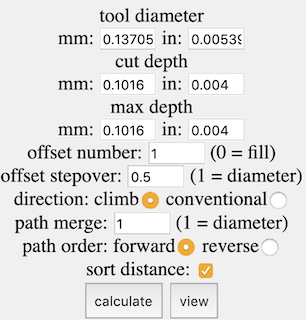
Then we can run the job on bCNC
For the cutouts the settings are the same as for the pads, except the tool diameter is 0.8.
Stuffing
Stuffing was quite challenging, it was my first time using 0805 parts, and that proved smaller then expected.
All in all I regret not having done more passes (say 2), making the tracks larger.
However, with some effort, it worked out.
Programming
For the programming, the first thing we do is import the right capacitive sensor library.
#include <CapacitiveSensor.h>
Set up the sender and sensor pin (correctly! see pins & anti-pins)
CapacitiveSensor capOne(8,9); // 8 is sender, 9 is sensor
Setup serial communication (in my case done through the arduino)
void setup()
{
  Serial.begin(9600);
}
The following could have been condensed into only void loop but this will make it easier for read & write using more sensors.
What it does is write to serial the value of the readings performed by cap.capacitiveSensor(30).
void check_state(CapacitiveSensor &cap)
{
  float read_val = cap.capacitiveSensor(30);
  Serial.print(read_val);
}

void loop()
{
  check_state(capOne);
  mySerial.print("\n");
  delay (50);
}
Arduino As A Programmer Can’t Read Serial
IF you try to connect the serial pins to an Arduino with a ArduinoISP program loaded on it,
the Tx & Rx pins won’t plot to serial monitor as they normally would.
To solve this issue, either connect to an alternative serial reader (like an FTDI cable) or load onto the Arduino something like BareMinimum under:
File->Examples->01.Basics->BareMinimum
This will free the Rx & Tx pins (don’t forget to detach the capacitor you inserted between RST & GND when you were programming the board)
The numbers should now plot onto the serial monitor as expected.
.... It sure is a headache, I get now why we use the FabISP.
Pins & Anti-pins
Initially, and somewhat foolishly, I thought I could upload this code “as is” to the board and have ZeroProblems™. This wasn’t the case. The basic code was correct, but the pin numbers were totally wrong!
It took me a while to figure this out by the way, the damn thing was uploading without a problem, yet the capacitative sensor was, well, not sensing.
As, I sat there crying for my incompetence in creating circuits, I was playing with the pin headers, moving them around in desperation and BOOM numbers appear.
The Arduino Pinout
We are all told from a young age “Arduino IDE pins match to the Arduino header labels, not the AVR on it”
Okay, cool, so if I have a LED connected to the Arduino pin header (not the ATTiny) 4, and I edit the Blink program from:
void setup() {
  // initialize digital pin LED_BUILTIN as an output.
  pinMode(LED_BUILTIN, OUTPUT);
}
to
led = 4
void setup() {
  pinMode(led, OUTPUT);
}
I expect the led to turn on. Now, I assumed this would be the case, I didn’t actually take out a LED to check if this is the case, but it worked with the hello echo.
We can confirm and backtrack this assumption by look at the DIP-28 package ATmega8/48/88/168/328 pinout -> Minicore to tell me that.
We can notice that Arduino pins 13, 12, 11, 10 match our programming wiring with SCK MISO MOSI SS and are mapped to IC pins 19 18 17 16,
so we can assume this mapping is correct, since we have been able to program the board.
So, in the above example code, pin 4 is actually IC pin 6.
The ATTiny44 Pinout
Using the reverse process, and a similar pinout diagram:
External link because image is too large, but compressing looses too much detail. Source, ATTinyCore
I can deduce that IC pin 2, which is my sender pin, is actually Arduino IDE pin 0 (or 10), which is the value I should set in the program.
However, looking at the actual pins that turn on, it turns out I had to look at PCINT not Arduino pin, which means the programming value should be 8 instead of 0 !

This was never an issue with the hello echo board because Arduino pins and PCINT match!
I’m not gonna lie, I’ve no idea why this is the case, but I just accepted as fact by now.
Conclusion
We can fix the pin-numbers in the otherwise correct code, and with that we close another chapter and my input device intakes.
(Code in porgramming section is correct)
Hero
Download The Files
-> Download The Inkscape Pads Design File
-> KiCad Design Files (Also Contains Design Files For TFT Board - week12)
-> Cap Over Serial .ino Code