9. Embedded programming
Assignment-1 Read Microcontroller datasheet
Introduction
The aim of this week was to understand the working of a microcontroller and learn to programme it to do our desired functions.
What is a Microcontroller ?
It all started here.A microcontroller is a single chip containing at least a CPU, non-volatile memory, volatile memory, a timer and an I/O control unit.The difference between a microcontroller and a regular PC is that the PC is a general purpose computer while a microcontroller is a computer dedicated to one or just a few tasks. It also has serial communication capabilities, interrupt controls and analog I/O capabilities.
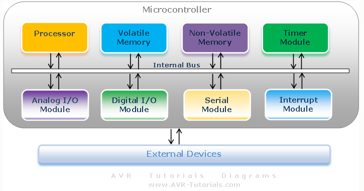
1) Processor - The processor refers to the Central Processing Unit (CPU) of the microcontroller. It contains the Arithmetic Logic Unit (ALU), Control Unit, Instruction Decoder and some Special Registers (Stack Pointer, Status Register, Program Counter, etc.).
2) Volatile Memory - This is memory used by the microcontroller for temporary data storage, system setup and peripherals configurations. Memory in this category includes SRAM and DRAM. AVR microcontrollers utilize SRAM.
3) Non-Volatile Memory - This is memory used by the microcontroller to store programs. Data can also be stored in this memory but the access time is much slower than that of RAM. Memory in this category includes ROM, PROM, EPROM, EEPROM and FLASH. The AVR microcontrollers utilize Flash for program storage, some AVR controllers contains a bit of EEPROM as well.
4) Timer Module - Most microcontrollers have at least one timer/counter peripheral. Timer/Counter modules are used to perform timing or counting operations in the controller. These include time stamping, measuring intervals, counting events, etc.
5) Interrupt Module - Interrupts enable the microcontroller to monitor certain events in the background while executing and application program and react to the event if necessary pausing the original program. This is all coordinated by the interrupt module.
6) Digital I/O Module - This module allows digital/logic communication with the microcontroller and the external world. Communication signals are that of TTL or CMOS logic.
7) Analog I/O Modules - These modules are use to input/output analog information from/to the external world. Analog modules include Analog Comparators and Analog-to-Digital Converters.
8) Serial Modules - These modules are used for serial communication with the external world.
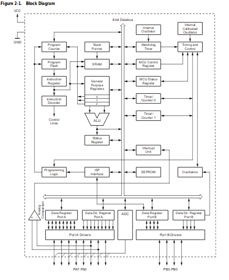
ATtiny44
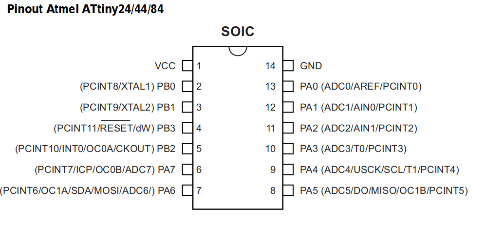
The picture above shows the schematic of ATtiny 44 microcontroller, an 8 bit Atmel microcontroller working on AVR enhanced RISC(Reduced Instruction Set Computing) modified Harvard architecture. Reading from the datasheet revealed following things. It means that microcontroller can simultaneously recieve and send 8 bits of data at a time.The resultingarchitecture is more code efficient while achieving throughputs up to ten times faster than conventional CISC microcontrollers.
The Memories and memory map
The memory map of a microcontroller is a diagram which gives the size, type and layout of the memories that are available in the microcontroller. The information use to construct the memory map is extracted from the datasheet of the microcontroller.
Types of memories
- In-System Re-programmable Flash Program Memory:
The Atmel ATtiny24/44/84 contains 2/4/8K bytes of on-chip, in-system, reprogrammable flash memory for program storage. Since all AVR instructions are 16 or 32 bits wide, the flash memory is organized as 1024/2048/4096 x 16.The flash memory has an endurance of at least 10,000 write/erase cycles. The Atmel ATtiny24/44/84 program counter (PC) is 10/11/12 bits wide, thus addressing the 1024/2048/4096 program memory locations.

-
SRAM Data Memory:
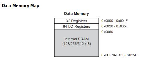 The lower 160 data memory locations address the register file, the I/O memory, and the internal data SRAM. The first 32 locations address the register file, the next 64 locations the standard I/O memory, and the last 128/256/512 locations address the internal data SRAM
 -
EEPROM Data Memory
The Atmel® ATtiny24/44/84 contains 128/256/512 bytes of EEPROM data memory. It is organized as a separate data space in which single bytes can be read and written. The EEPROM has an endurance of at least 100,000 write/erase cycles.
Source : http://www.avr-tutorials.com
AVR Stack & Stack Pointer
What is a stack?
A stack is a consecutive block of data memory allocated by the programmer. This block of memory can be use both by the microcontroller internal control as well as the programmer to store data temporarily. The stack operates with a Last In First Out (LIFO) mechanism, i.e the last thing store on the stack is the first thing to be retrieved from the stack.
What is the Stack Pointer?
The stack pointer is basically a register or registers that holds either “the memory address of the last location on that stack where data was stored” or “the memory address of the next available location on the stack to store data.” The definition of the stack pointer depends on the design of the microcontroller.
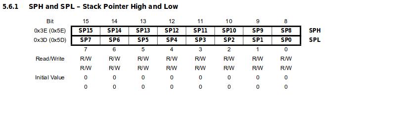
The AVR Stack Pointer
The AVR 8-bits microcontroller stack pointer can either consist of a single I/O register SPL (Stack Pointer Low) or two (2) I/O registers SPL and SPH (Stack Pointer High). In ATtiny 44 the latter is used. The size of the stack pointer depends on the amount of data memory a microntroller contains. If the entire data memory can be addressed using 8-bits then the stack pointer is 8-bits wide i.e. SPL only, otherwise the stack pointer is consist of SPL and SPH.
ALU – Arithmetic Logic Unit
The high-performance Atmel AVR ALU operates in direct connection with all 32 general purpose working registers. Within a single clock cycle, arithmetic operations between general purpose registers or between a register and an immediate are executed. The ALU operations are divided into three main categories - arithmetic, logical, and bit functions. Some implementations of the architecture also provide a powerful multiplier supporting both signed/unsigned multiplication and fractional format.
Status Register
The status register contains information about the result of the most recently executed arithmetic instruction. This information can be used for altering program flow in order to perform conditional operations. Note that the status register is updated after all ALU operations, as specified in the instruction set summary. This will in many cases remove the need for using the dedicated compare instructions, resulting in faster and more compact code.
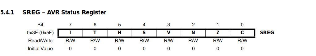
 Description of various bits in SREG register
AVR Digital I/O
Associated I/O registers
AVR Register ?
All information in the microcontroller, from the program memory, the timer information, to the state on any of input or output pins, is stored in registers. Registers are like shelves in the bookshelf of processor memory. In an 8-bit processor, like the AVR ATMega 16 we are using, the shelf can hold 8 books, where each book is a one bit binary number, a 0 or 1. Each shelf has an address in memory, so that the controller knows where to find it.
Source:https://ccrma.stanford.edu/workshops/pid2004/lectures/programming/programming/AVR_Registers.html
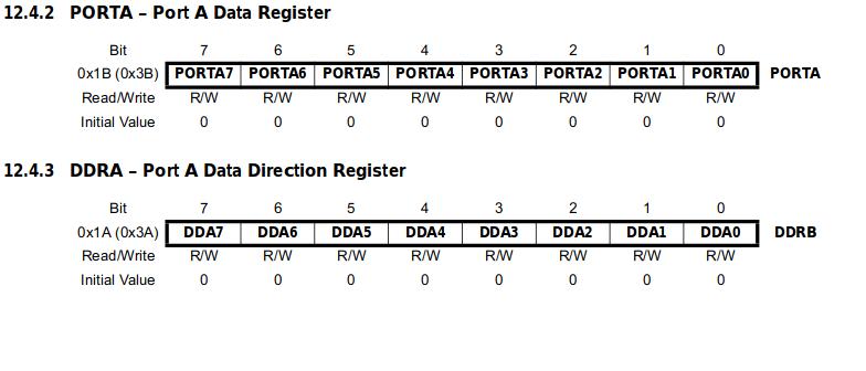
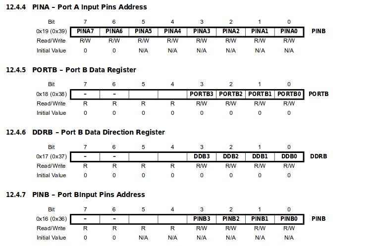
Each of the AVR Digital I/O ports is associated with three (3) I/O register. A Data Direction Register (DDRx), A Pin Register (PINx) and a Port Register (PORTx). Where x is the port A, B, C, etc.
- DDRx - Port X Data Direction Register

DDRx is an 8-bit register which stores configuration information for the pins of Portx. Writing a 1 in the pin location in the DDRx makes the physical pin of that port an output pin and writing a 0 makes that pin an input pin.
Note: Each physical pin of a port is configured independently and thus a port can have some of its pins configured as input an the others as output pins.
- PINx - Port X Input Pins Register

PINx is an 8-bit register that stores the logic value, the current state, of the physical pins on Portx. So to read the values on the pins of Portx, you read the values that are in its PIN register.
- PORTx - Port X Data Register

PORTx is an 8-bit register which stores the logic values that currently being outputted on the physical pins of Portx if the pins are configured as output pins. So to write values to a port, you write the values to the PORT register of that port.
 Registers in AT tiny 44
The DDRx register is use to configure the pins on portx as input or output pins. Each pin on a port is independent and thus the entire port does not have to be configured totally as an input or output port. Writing a 1 in the pin position in the DDRx will configure that pin as an output pin and writing a 0 will configure the pin as an input pin.
Logic values written to the PORTx register is outputted to the pins on Portx that are configured as output pins.
Logic values read from the PINx register is equivalent to the values presently on the pins of Portx which are configured as input pins.
AVR Microcontroller Interrupts
What are interrupts?
Interrupts are basically events that require immediate attention by the microcontroller. When an interrupt event occurs the microcontroller pause its current task and attend to the interrupt by executing an Interrupt Service Routine (ISR) at the end of the ISR the microcontroller returns to the task it had pause and continue its normal operations.An Interrupt Service Routine (ISR) or Interrupt Handler is a piece of code that should be execute when an interrupt is triggered. Usually each enabled interrupt has its own ISR.
In order for the microcontroller to respond to an interrupt event the interrupt feature of the microcontroller must be enabled along with the specific interrupt. This is done by setting the Global Interrupt Enabled bit and the Interrupt Enable bit of the specific interrupt.
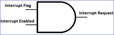
Interrupt Flags and Enabled bits
Each interrupt is associated with two (2) bits, an Interrupt Flag Bit and an Interrupt Enabled Bit. These bits are located in the I/O registers associated with the specific interrupt:
-
The interrupt flag bit is set whenever the interrupt event occur, whether or not the interrupt is enabled.
-
The interrupt enabled bit is used to enable or disable a specific interrupt. Basically is tells the microcontroller whether or not it should respond to the interrupt if it is triggered.
In summary basically both the Interrupt Flag and the Interrupt Enabled are required for an interrupt request to be generated as shown in the figure below.
Global Interrupt Enabled Bit
Apart from the enabled bits for the specific interrupts the global interrupt enabled bit MUST be enabled for interrupts to be activated in the microcontoller.
For the AVR 8-bits microcontroller this bit is located in the Status I/O Register (SREG). The Global Interrupt Enabled is bit 7, the I bit, in the SREG.
7th bit I
Interrupt sources provided with the AVR microcontroller
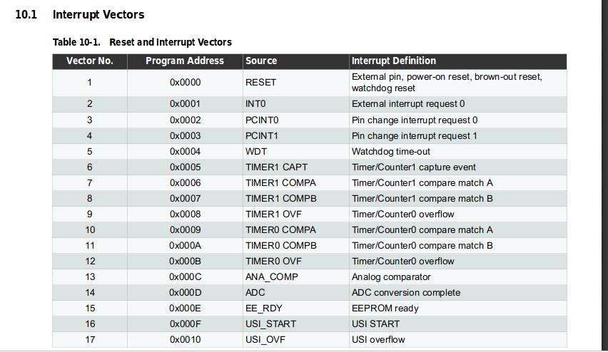
The AVR 8-bits microcontroller provide both internal and external interrupt sources. The internal interrupts are associated with the microcontroller’s peripherals. That is the Timer/Counter, Analog Comparator, etc. The external interrupts are triggered via external pins. The figure below shows the pins, on which the external interrupts can be triggered, for an AVR 8-bit ATtiny 44 microcontroller. On this microcontroller there are 12 external interrupts PA0…11.
An interrupt vector is the memory address of an interrupt handler. The interrupt vector for each interrupt provided by the AVR microcontrollers can be found in its datasheet.
AVR Microcontroller Analog Input/Output
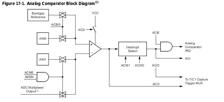
A number of the Atmel AVR 8-bits microcontroller provide analog input/output (I/O) capabilities through their “Analog Comparator” and “Analog to Digital Converter (ADC).”
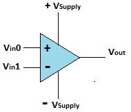
What is an analog comparator?
An analog comparator is a device that compares two (2) analog values and indicate which is greater. In electronics it is basically an amplifier without feedback and thus very high gain, as shown below. When the positive input (+) is greater the output voltage is saturated to its positive supply (logic 1), otherwise the output is saturated to is negative supply ( logic 0).
That is: “Vout = logic 1” when “Vin0 > Vin1” and “Vout = logic 0” when “Vin0 < Vin1”.
The ATtiny24A/44A/84A provides the following features: 2K/4K/8K byte of In-System Program-mable Flash, 128/256/512 bytes EEPROM, 128/256/512 bytes SRAM, 12 general purpose I/Olines, 32 general purpose working registers, an 8-bit Timer/Counter with two PWM channels, a16-bit timer/counter with two PWM channels, Internal and External Interrupts, a 8-channel 10-bitADC, programmable gain stage (1x, 20x) for 12 differential ADC channel pairs, a programmableWatchdog Timer with internal oscillator, internal calibrated oscillator, and four software select-able power saving modes. Idle mode stops the CPU while allowing the SRAM, Timer/Counter,ADC, Analog Comparator, and Interrupt system to continue functioning. ADC Noise Reductionmode minimizes switching noise during ADC conversions by stopping the CPU and all I/O mod-ules except the ADC. In Power-down mode registers keep their contents and all chip functionsare disbaled until the next interrupt or hardware reset. In Standby mode, the crystal/resonatoroscillator is running while the rest of the device is sleeping, allowing very fast start-up combinedwith low power consumption.
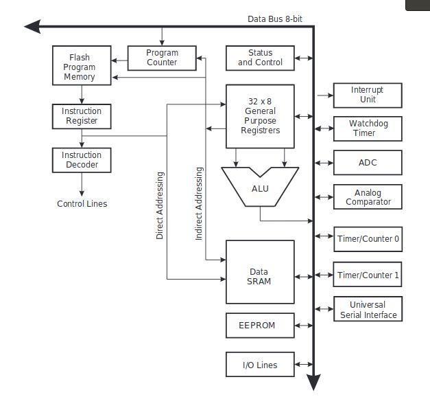 Harvard Architecture
Program counter
The Program Counter (PC) is a register that is apart of all central processing unit (CPU) or microprocessor. All microcontrollers contains a microprocessor and thus has a program counter. The purpose of the program counter is to hold/store the address of the next instruction to be executed by the microcontroller’s microprocessor.The size (width) of the program counter of a microcontroller is measured in bits and is directly related to the size of the microcontroller’s program memory.
The width(size) of the program counter (PC) is basically the smallest possibly number of bits necessary to address the microcontroller program memory based on its organisation. Lets say n is the width of the PC then n would be related to the size of the program memory by the following equation:
2^n = size of program memory n = log(size of program memory)/(log2)
Programming the MCU
Using C
The basics of C programming was learnt from http://www.avr-tutorials.com/digital/digital-input-output-c-programming-atmel-avr-8-bits-microcontrollers
A simple programme was used to keep the LED blinking
First part was to install GCC compiler to use the C language by typing the following command in the terminal
sudo apt install gcc
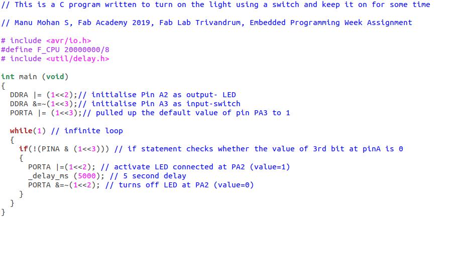
1) Wrote a programme in C to keep the LED blinking. It was noted that my LED is connected to PB2.
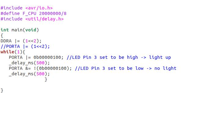
Being a beginner in C, it was my first attempt. Our lab instructor Yedu did really help mostly all with this program. I am gonna try myself in improvising this and build a new one !.
2) Made a Makefile which necessarily involved following commands
        `file_name = main

        device  = attiny44

        object:
             avr-gcc -g -Os -mmcu=$(device) -c $(file_name).c

        link:
             avr-gcc -g -mmcu=$(device) -o $(file_name).elf $(file_name).o

        hexfile:
             avr-objcopy -j .text -j .data -O ihex $(file_name).elf $(file_name).hex


        hex: object link hexfile`
I understood that the make file is something like of a shortcut to execute so many commands. At the end we can see that command hex will run all the commands sequentially referred by object, link and hexfile. The aim is to make a hex file that instructs the MCU to perform our desired operation mentioned in the program.
3) First thing is to make the hex file. Typed make hex. A hex file was made.
4) Flashing the MCU with the hex file made by using the command avrdude -p t44 -c usbtiny -U flash:w:main.hex in the terminal where the folder containing the hex file.
It didn’t work, sadly it kept on returning connection rc-1 error !. I was so preoccupied that I forgot to screen shot it. Connections was checked with a multimeter, it’s all working.
It took me a while with the help of our Instructor that the fault was that my pin is connected to the same port as to the one pin of the external oscillator.
Solution was that the free pin PA2 was used to connect the LED port! Let’s see if it works
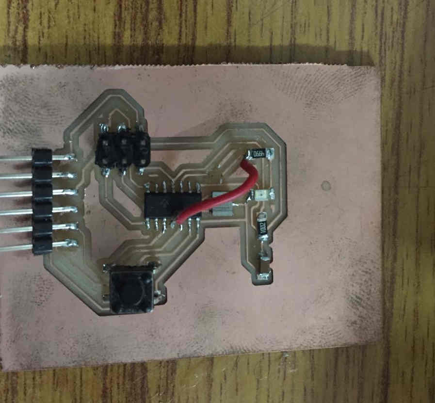 See the red wire used to by pass the conenction. Thankyou Suhail P for your timely help. I think I spent some 2 hours on this !
Video here
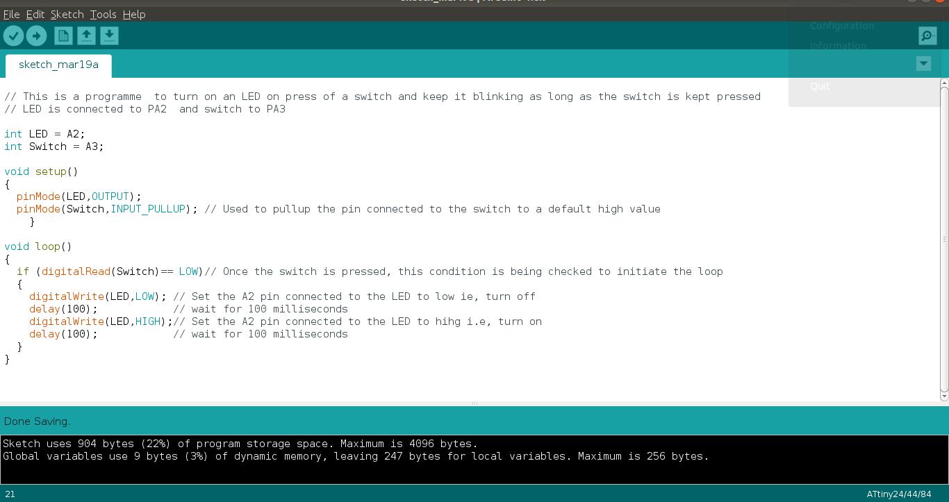
Attempt -2 using with switch
Opened Atom, the best text editor
Did programming to make a switch so that when we push, it will blink for some time and turnoff at the next push.
It worked !
Using Aurdino IDE
The Arduino integrated development environment (IDE) is a cross-platform application (for Windows, macOS, Linux) that is written in the programming language Java. It is used to write and upload programs to Arduino board.
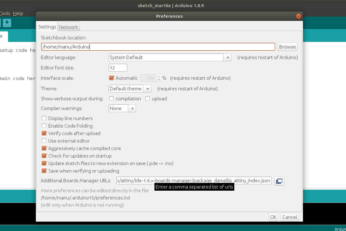
Configuring Aurduino 1) Install Aurduino IDE for Linux 64 bit.
2) Go to File, Preferences and add additional board manager url as https://raw.githubusercontent.com/damellis/attiny/ide-1.6.x-boards-manager/package_damellis_attiny_index.json
3)In the Tools select the following
1) Select the parameters to the follwoing
Board to ATtiny44
Processor to ATtiny44
Clock to External 20Mhz
Programmer to USB tiny ISP
2) After writing the code the use Verify/Compile tab in Sketch menu and if successful use Upload to flash the program onto the microcontroller.
Compared to C language Aurduino IDE was found to be more easier to learn and use. But I understood that the C is the basic one. For doing complex programs we will have to rely on C programming.
Further
-
How can I use it to program my board for final project was the next point. I would be using atleast two sensors to simultaneously along with a possible lcd display outside.
-
Learnt that Aurdino libraries are costly when we burn the MCU that they take more flash memory in the MCU.
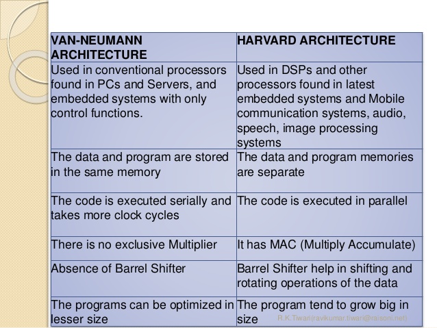
Assignment-2 Comparision of Different architecture
Above part we have seen MCU based on modified Harvard Architecture. We were given a comparison tour through another different architecture which was Von Neumann Architecture.
Below you will find key performance and functional variations with the new Harvard Architecture.
The picture below shows the Performance difference between the two architectures
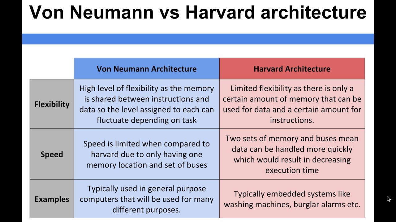 Image Source :Youtube.com
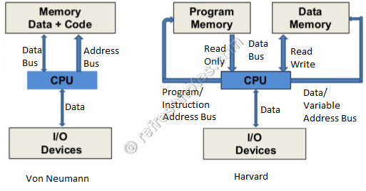
 Comparison based on the working
Comparison based on development workflow
Source:https://www.refreshnotes.com/2016/02/von-neumann-vs-harvard-architecture.html
Microbit and Rasperrypie
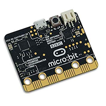
Source https://www.amazon.co.uk/BBC-MB80-micro-bit/dp/B01G8WUGWU)
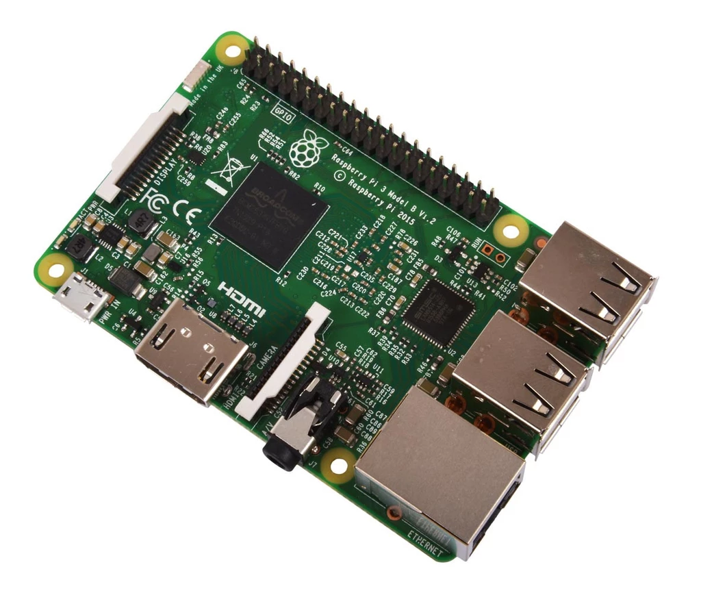
Source(https://thepihut.com/products/raspberry-pi-3-model-b)
Both are opensource ARM based embedded system designed for educational purpose.
ARM architecture
ARM, previously Advanced RISC Machine, originally Acorn RISC Machine, is a family of reduced instruction set computing (RISC) architectures for computer processors, configured for various environments. Arm Holdings develops the architecture and licenses it to other companies, who design their own products that implement one of those architectures—including systems-on-chips (SoC) and systems-on-modules (SoM) that incorporate memory, interfaces, radios, etc. It also designs cores that implement this instruction set and licenses these designs to a number of companies that incorporate those core designs into their own products. Processors that have a RISC architecture typically require fewer transistors than those with a complex instruction set computing (CISC) architecture (such as the x86 processors found in most personal computers), which improves cost, power consumption, and heat dissipation. These characteristics are desirable for light, portable, battery-powered devices—including smartphones, laptops and tablet computers, and other embedded systems
What is RISC Architecture ?
Reduced Instruction Set Computer (RISC) is a type or category of the processor, or Instruction Set Architecture (ISA). Speaking broadly, an ISA is a medium whereby a processor communicates with the human programmer (although there are several other formally identified layers in between the processor and the programmer). An instruction is a command given to the processor to perform an action. An instruction set is the entire collection of instructions for a given processor, and the term architecture implies a particular way of building the system that makes the processor.
RISC generally refers to a streamlined version of its predecessor, the Complex Instruction Set Computer (CISC). At the dawn of processors, there was no formal identification known as CISC, but the term has since been coined to identify them as different from the RISC architecture. Some examples of CISC microprocessor instruction set architectures (ISAs) include the Motorola 68000 (68K), the DEC VAX, PDP-11, several generations of the Intel x86, and 8051.
Examples of processors with the RISC architecture include MIPS, PowerPC, Atmel’s AVR, the Microchip PIC processors, Arm processors, RISC-V, and all modern microprocessors have at least some elements of RISC. The progression from 8- and 16-bit to 32-bit architectures essentially forced the need for RISC architectures. Nevertheless, it took a decade before RISC architectures began to take hold, mainly due to lack of software that would run on RISC architectures. Intel also made an impact, since it had the means to continue using the CISC architecture and found no need to redesign from the ground up. The MIPS architecture was one of the first RISC ISAs and has been used widely to teach the RISC architecture.
The table below shows a comparison of the RISC and CISC architecture.
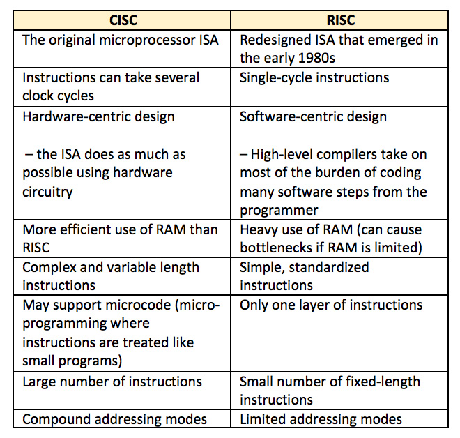 Source:https://www.microcontrollertips.com/risc-vs-cisc-architectures-one-better/
References
1.http://www.avr-tutorials.com/general/microcontrollers-basics
2.https://en.wikipedia.org/wiki/AVR_microcontrollers
3.http://ww1.microchip.com/downloads/en/devicedoc/Atmel-7701_Automotive-Microcontrollers-ATtiny24-44-84_Datasheet.pdf