Week 7
Electronic Design !
MOOD OF THE WEEK
This week was pretty difficult for me. As I want to try new stuff, I decided to hand draw my circuit. Of course, it didn't work as well as I hoped. But, as I am a stubborn person, I went to the end of it and even if it didn't turn that well I am glad I did. I learnt a lot and I know I'll try again until it works out :)
Electronic Design
This week's assignments :
- Group assignment
- use the test equipment in your lab to observe the operation of a microcontroller circuit board
- Han Solo assignments :
- redraw the echo hello-world board
- add (at least) a button and LED (with current-limiting resistor)
- check the design rules, make it, and test it
Group Assignment
Here is the link to our documentation for the group assignment : http://fabacademy.org/2019/labs/sorbonne/group_work/electro_design/
Han Solo Assignment
This week, we have to make our own PCB design. We have to redo the Hello Board, but with our own roads and stuff. And we have to add a button and a led.
During Neil’s lecture, he presented this project that I liked a lot : http://fab.cba.mit.edu/classes/863.15/section.CBA/people/Schaad/week6-electronics-design.html
As I like it the “easy way”, I decided to try and do the same kind of hand drawn PCB :)
Step 0 : having an Eagle file anyway
Let’s do a schematic on Eagle. Wanna know how Eagle works ? You can follow my Eagle Tutorial so you can do your own PCB :)
Step 1 : understanding the process to draw the circuit and end up with a rml file
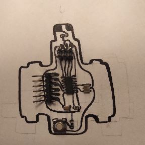
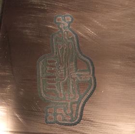
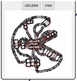
First things first, I milled a test just to see if the process I have in mind works. I took the original Hello Board from Eagle, and draw it. Pen and paper, here I am ! :)
I tried several things, from more complex to simpliest ones. I took the simpliest one as a start (the one you see right below).
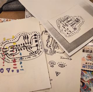
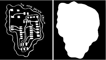
I then scanned it to be able to play with the drawing and vectorize it.
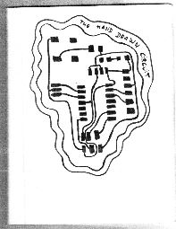
I did it with Krita and Inkscape, and saved them as PNG files. Here are the results !
I’m pretty happy with it !
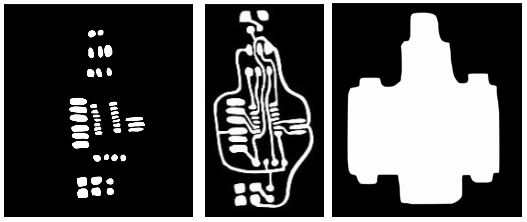
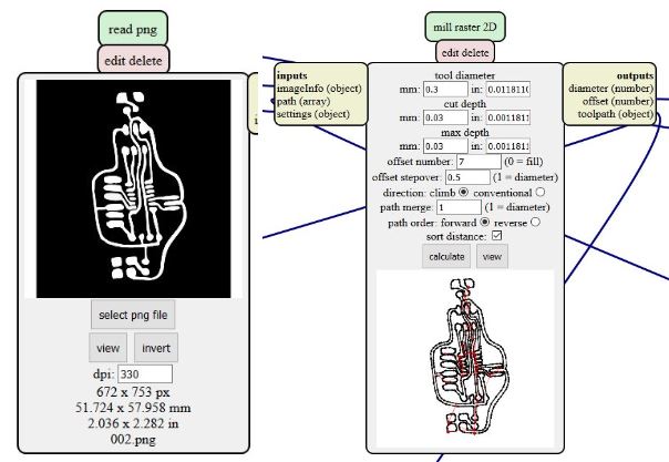
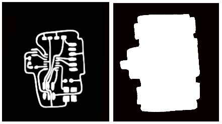
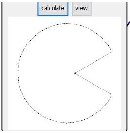
Now, let’s see if it works on mods now. I can say that when mods started calculating, it was a real thrill to see all the roads being drawn :) I used the same settings as in the electronic production week.
A really important thing that I learnt ! : When you hand draw your circuit like this, in mods do not forget to change the DPI. When I started milling, I didn’t understand on the first trys why the circuit was so big. It was because I didn’t change the DPI and the size of my board.
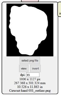
Be careful to have the same dimensions on the inline and the outline.
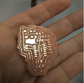
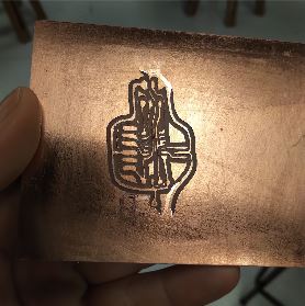
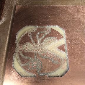
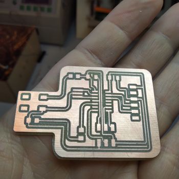
Now that I’ve settled that, I can mill my board. And I just looooooove how it came out :)
Let’s now assemble all of our components to try them on the board :)
-
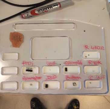
We need :
- 1 x FTDI
- 1x led
- 2 x 470 resistors
- 1 x ISP
- 1 x button
- 1 x 1 x resonator
- 1 x 1uf capacitor
- 1 x 10k resistor
- 1 x ATtiny 44
This made me realize one thing I didn’t thought about before, is the size of the components vs size of the board. They are too small for my board, but I’m glad coz I’m close to the actual size ! I have to be careful for the real one though !
Step 2 : trying with the good proportions and with soldered components
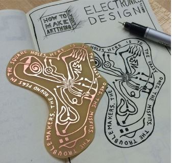
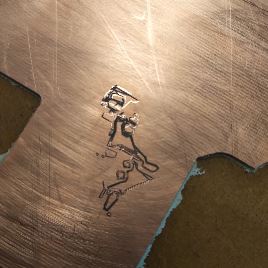
I want to put the led inside the 3D design I did last week. I want my PCB to be shaped like a spaceship :)
First, the measures ! As I saw on my test that the components were not at the right size, I took the time to measure them to make sure they will be the right size, and to design my spaceship around it.
I did the roads with a pen first, and then a felt. Here is what it looks like in the end !
Okay, now the tricky part : cleaning all this and import it in mods ! :) Only the components, with the roads and finally the outline :
Importing in mods, being careful with the DPI and starting the calculation…. Here’s the result in mods :)
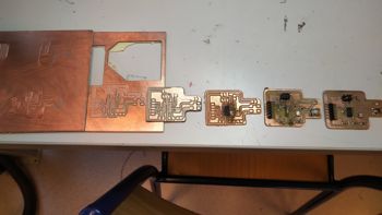
Let’s start the milling ! I thought this would be easy, just launch the milling and everything will be fine ! How naive I am ^^’ Little did I know that would be the start of a loooooot of failures ^^’
But failing means learning right ? So let’s try to understand what happened ! On this one, the mill was barely touching the copper plate, except at some points…
My settings seemed correct. Maybe it’s a problem with the tape I used for the board, this seems to show that it worked at some places and not others. Let’s try with another one and taped differently !
Yeah ! It works perfectly !
BUT…. (coz there’s always a but).... my roads are wrong ^^’ I showed my design to Adel that pointed at me correctly that my button and my led were connected to…. well nothing ^^’
Okay…. patience patience, let’s do it again ! I took a look on Adel’s board from last year and tried to reproduce it, and adapt it to my design.
And yet …. still not there …. My board didn’t work…. AGAIN.
After redoing it over and over again, I tried from scratch, thinking maybe my design was the issue (since I did some of the roads by hand and others on the computer). I tried with something a bit bigger, different. Hope it will work this time ^^
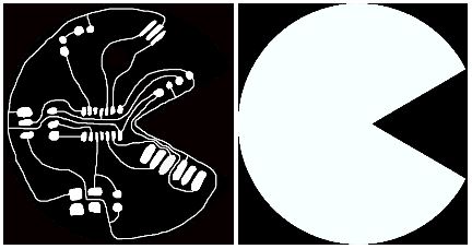
Roads are clear, components at the right size…. okay this one is for good … Or not ! I had trouble with my settings this time, engraving my pacman instead of cutting it ^^’
I have to make myself some setting rules, I think I didn’t quite got it yet how the milling machine works to mill the roads and stuff.
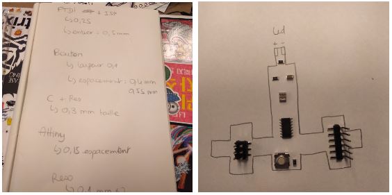
Here are the correct settings for this PCB :
-
module configuration for traces :
- tool diameter: 0.3 mm
- cut depth: 0.03 mm
- max depth: 0.03 mm
- offset number: 7
-
module configuration for outlines :
- tool diameter: 1.5 mm
- cut depth: 0.4 mm
- max depth: 1.7 mm
- offset number: 1
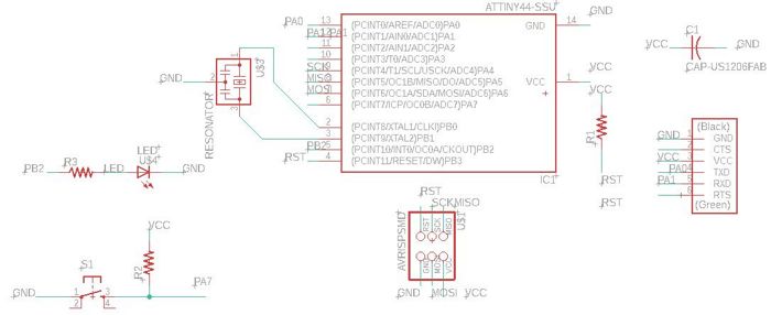
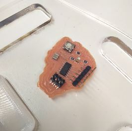
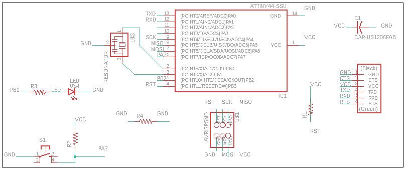
UPDATE : I MADE IT WORK YOUHOU !
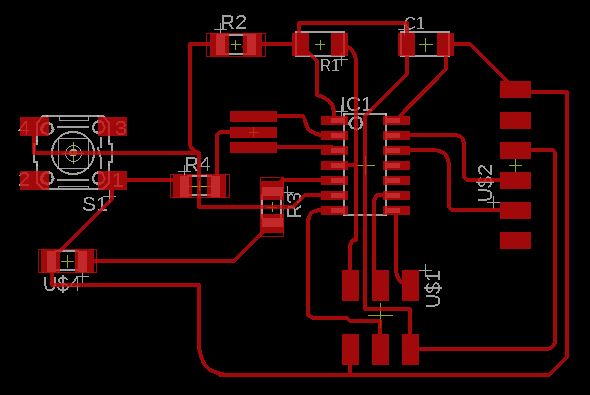
I abandonned for now drawing my PCB by hand... but only for now ! And after some weeks of despair, I finally made it work ! :) Here are the schematic and design of my new Hello Board.
I think this is what you call progression ^^