9. Embedded programming
The goal for this week as an individual assignment was to:
- read a microcontroller data sheet
- program the board to do something
- try as many different programming languages and programming environments as possible.
- My responsibility was to programme the board I had designed during the electronics design week and to make the button and led work.
Project Research
This week i also started researching on what i need for my project. With milling of PCB and basic understanding of electronics i started searching on how i can build a food computer. What i will need to make electronis work and plan upcoming weeks.
Food computer has following key electronics components
- A Brain which is written in Python code and works on Raspberry Pi
- A arudino based microcontroller to read sensor data
- Various sensors like temperature, humidity, soil sensor etc.
- Display to show sensor data
- Connection to Alexa
A community 300 dollar version that i am targetting in upcoming weeks
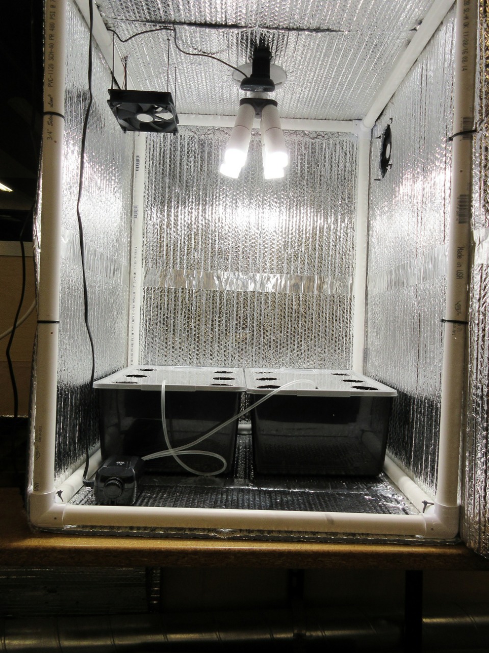
I used earlier year project work reference from Guillaume Teyssié who designed an aquaponics system. And seems like its what i need for food computer too. It uses Arduino based microcontroller that can be fabricated in fablab , uses Raspberry Pi and i already know how to hook up AWS alexa with a Raspberry pi
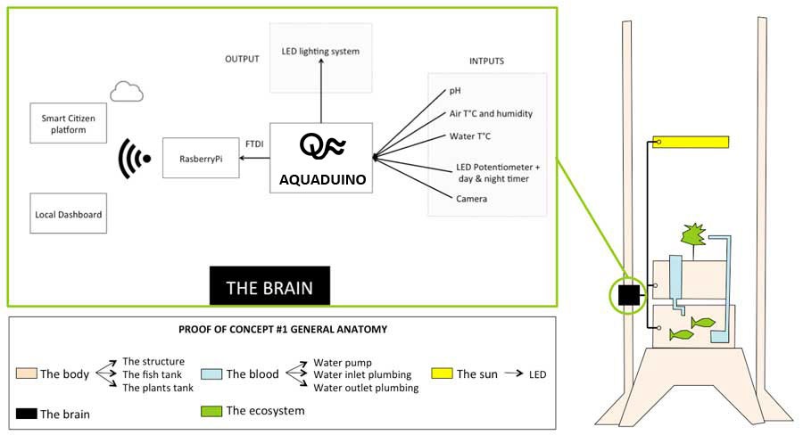
I discussed with my reviewer Suhas (Vigyaan Ashram) the idea how to start working on my project and he helped me draw a high level diagram and gave me insight on which sensors available in fab lab that i can target in upcoming weeks for input and output.
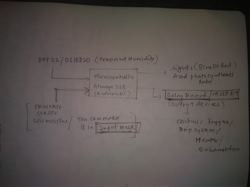
Temperature and Humidity Sensor
Read a Microcontroller DataSheet
Once it was clear that i need Atmgea microcontroller for my project and i am already comfortable with Arduino and Raspbery pi i should target arduino based microcontroller for my project. For this i started going through the datasheet and referred for fablab earlier year students who have used Atmgea328p in embedded programming week and i found one tanja-lovric.
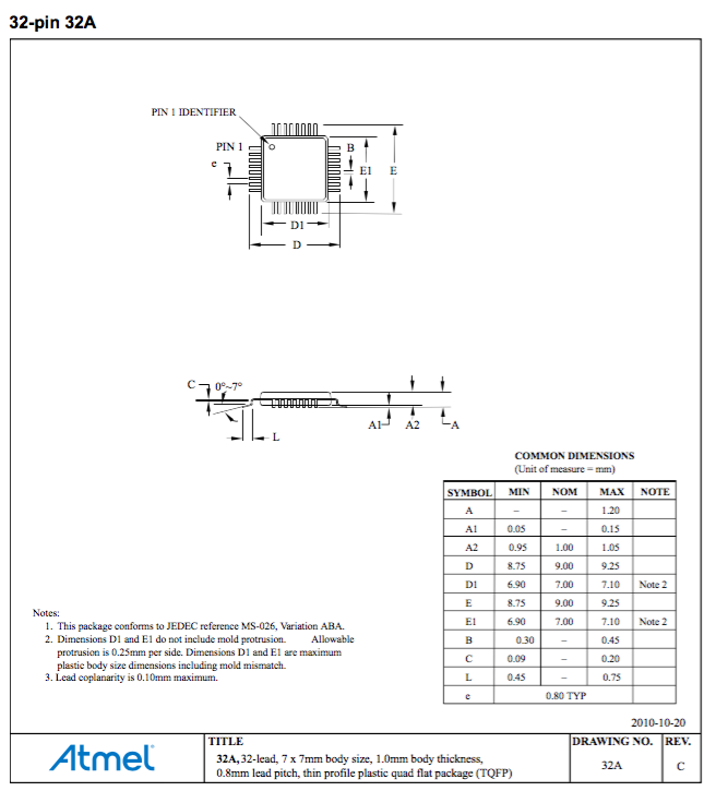
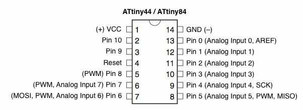
ATmega 328p-AU Understanding that i got from Tanja lovric page
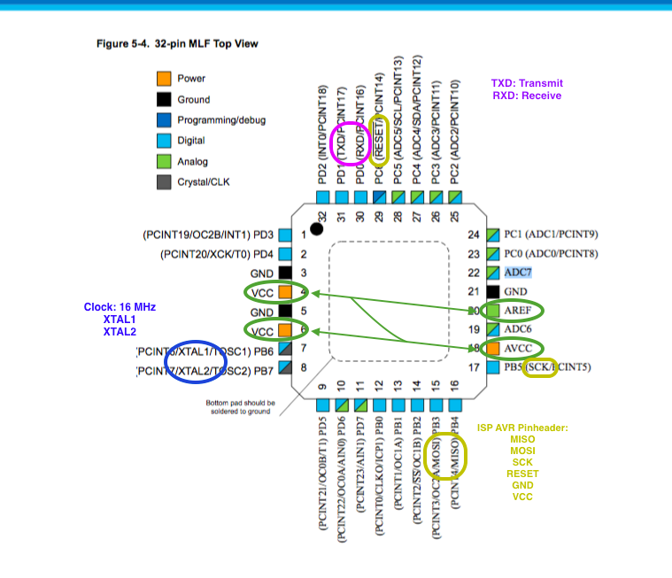
- VCC Digital supply voltage.
- GND: Ground
- AVCC: AVCC is the supply voltage pin for the A/D Converter, PC[3:0], and PE[3:2]. It should be externally connected to VCC, even if the ADC is not used. If the ADC is used, it should be connected to VCC through a low-pass filter. Note that PC[6:4] use digital supply voltage, VCC.
- AREF AREF is the analog reference pin for the A/D Converter. 5.2.9. ADC[7:6] (TQFP and VFQFN Package Only).In the TQFP and VFQFN package, ADC[7:6] serve as analog inputs to the A/D converter. These pins are powered from the analog supply and serve as 10-bit ADC channels.
- RESET (PC6):If the RSTDISBL Fuse is programmed, PC6 is used as an I/O pin. Note that the electrical characteristics of PC6 differ from those of the other pins of Port C. If the RSTDISBL Fuse is unprogrammed, PC6 is used as a Reset input. A low level on this pin for longer than the minimum pulse length will generate a Reset, even if the clock is not running. Shorter pulses are not guaranteed to generate a Reset. The various special features of Port C are elaborated in the Alternate Functions of Port C section.
- XTAL1/XTAL2 (Port B): Port B is an 8-bit bi-directional I/O port with internal pull-up resistors (selected for each bit). The Port B output buffers have symmetrical drive characteristics with both high sink and source capability. As inputs, Port B pins that are externally pulled low will source current if the pull-up resistors are activated. The Port B pins are tri-stated when a reset condition becomes active, even if the clock is not running. Depending on the clock selection fuse settings, PB6 can be used as input to the inverting Oscillator amplifier and input to the internal clock operating circuit.
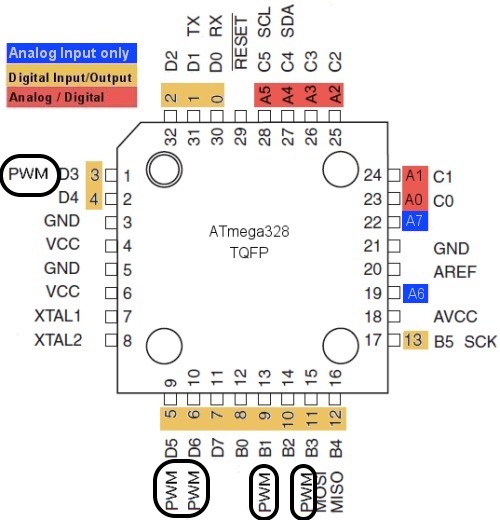
- Below image shows the spread of the PWM-Pins, digital and analog pins of ATmega328p-AU. PWM (Pulse Width Modulation) pins are important for the control of analog devices such as RGB LED or for transfer of sensing data over long distances. Using PWM we can also regulate the intensity of the light and control of DC motors.
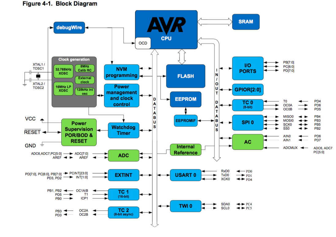
- Below you can see the block diagram how the output and input pins are connected to the CPU /(Central Processing Unit).
More Details Around Microcontroller
To get more understanding on microcontroller i purchased following book. Its a nice book to get started with AVR programming and build some DIY projects. As software is not a chalenge for me, i spent my time understanding the hardware side of things.
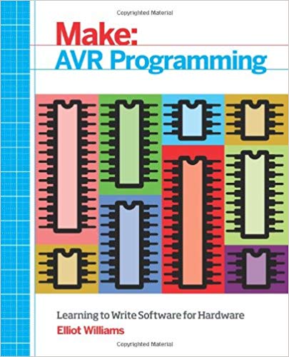
Below are some of the abstract from the book.
- Microcontroller is A Computer on a Chip…
Microcontrollers are often defined as being complete computers on a single chip,and this is certainly true.At their core, microcontrollers have a processor that is similar to the CPU on your computer. The processor reads instructions from a memory space (in flash memory rather than on a hard drive), sends math off to an arithmetic logic unit (instead of a math coprocessor), and stores variables in RAM while your program is running.Many of the chips have dedicated serial hardware that enables them to communicate to the outside world.Like any computer, you have the option of programming the microcontroller using a variety of languages.So microcontrollers are just tiny little computers on a chip.
- I also came to know about the RAM capability in microcontrollers
One thing to notice is that the chips in the AVR product line, from ATtiny15 to ATmega328, include the flash program memory space in kilobytes in the chip’s name. Yeah, you read that right: we’re talking about 1 KB to 32 KB of room for your code. Because of this limited program memory space, the scope of your program running on a single chip is necessarily smaller than, for example, that Java enterprise banking system you work on in your day job. Microcontrollers have limited RAM as well. The ATmega168 chips that we’ll be focusing on here have a nice, round 1 KB
Key learings
- Microcontroller is a small computer
- Memory is quite less few KB
- AVR family of microcontrollers have 8-bit CPUs without a floating-point math coprocessor inside. This means that most of the math and computation you do will involve 8-bit or 16-bit numbers
- So a microcontroller is a self-contained, but very limited computer—halfway between a computer and a component
- Microcontroller does all the work by reading voltages applied to its various pins or by setting up output voltages to these very same pins. Blinking an LED is an obvious example so when the output voltage is high, the LED lights up, and when the voltage is low, it doesn’t
- I understood the basic of some key components in a microcontoller CPU, Memory (Flash, RAM, EEPROM, Clock, Outputs). Most important is input and output how you can program the pins to get impact in physical world. Seems like for reading sensor data i need to use input pins and for displaying my data or communicate i need to use output pins.
- One of the most important learning i got is when to use datasheet. As per book the datasheets don’t seem helpful at first—the datasheet tells you everything about how the chip works, but almost nothing about how you should work with the chip. Some sections of the datasheets are nearly impenetrable unless you already know the basics of what’s going on inside the chip already. The trick is to approach the datasheet like a reference book rather than a novel.
- Overall this book is a good resource for my future projects. I recommend my fellow students to buy this one.
Embedded Programming
Onec i got some basic understanding from datasheet and book on microcontroller next step was to program my hello board that i developed as part of electronics design week.
The words “program,” “programmer,” and “programming” are overloaded in the microcontroller world. We (as programmers) write programs, compile them, and then use a flash programmer to program the AVRs, which then runs our program
Toolchain overview
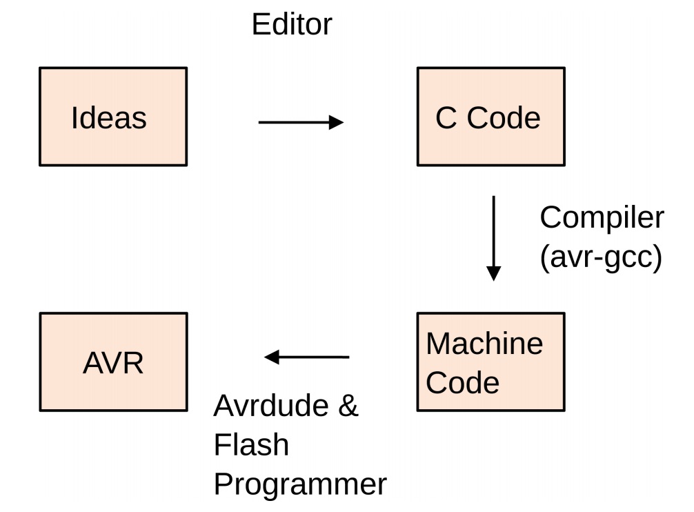
Getting code from computer screen to a working piece of electronic machinery requires a chain of tools called toolchain.
Steps that we need to make it work
- First we write source code in an editor.
- Then we convert the source code into machine code with a compiler (and associated software tools). avr-gcc, is the AVR-specific version of the popular open source compiler GCC.
- Then using uploader software(like AVRDUDE) on computer and a hardware flash programmer( The flash programmer is a piece of hardware that sits in between your computer and the target AVR microcontroller), send the machine code to target AVR chip, which stores the instructions in its nonvolatile flash memory. The AVR microcontrollers, when put into programming mode, listen over their serial peripheral interface (SPI) bus for incoming data to flash into program memory. The flash programmer’s job is to relay the compiled machine code to the target AVR over the SPI bus
- As soon as the flash programmer is done, the AVR chip resets and starts running the code.
Using Arduino IDE to Blink a LED
As for my project the target i am looking is to build a arduino based microcontroller, i wanted to familarise myself with Arudino IDE.
Here is very good link on how program Atttiny.
Steps:
-
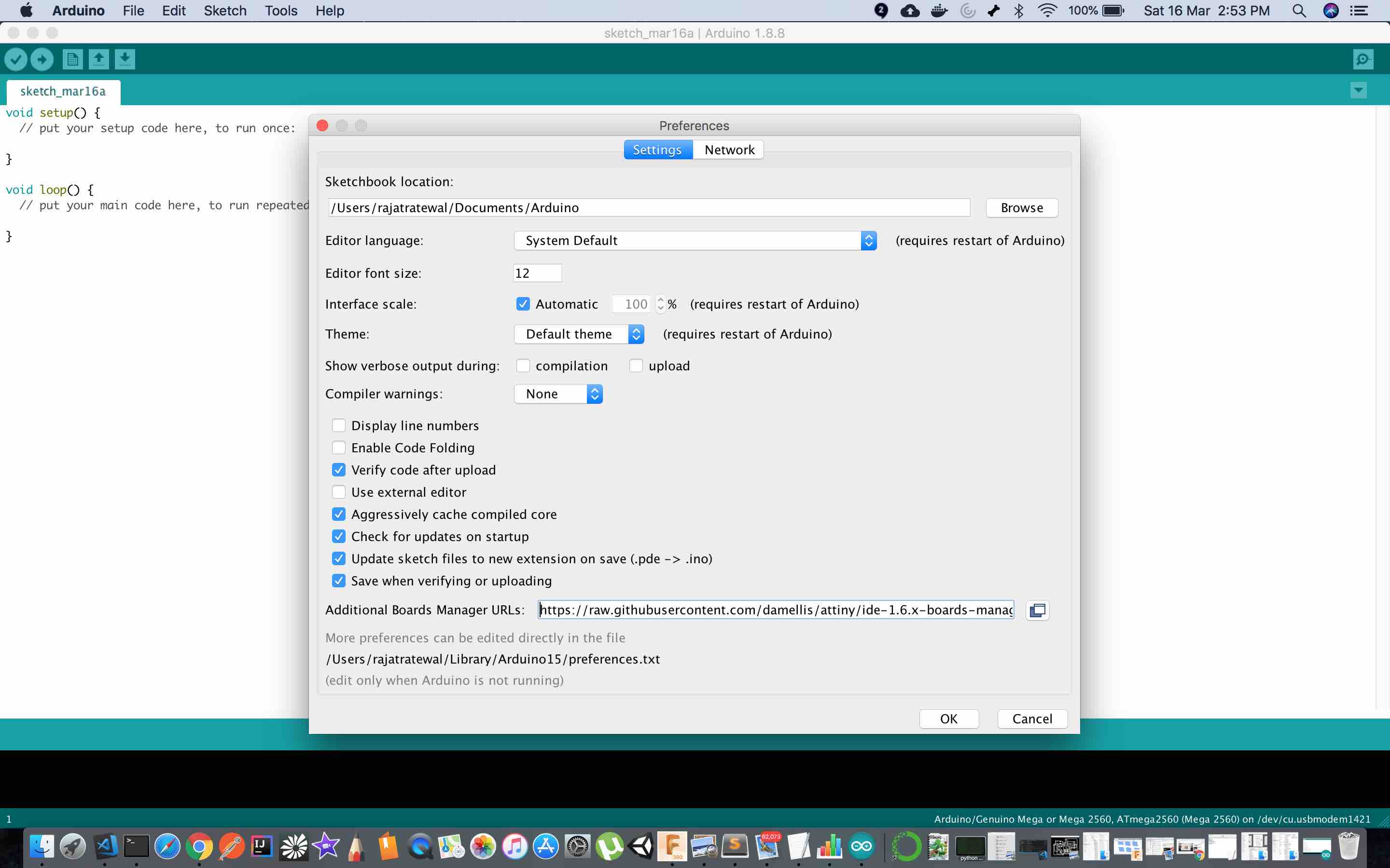
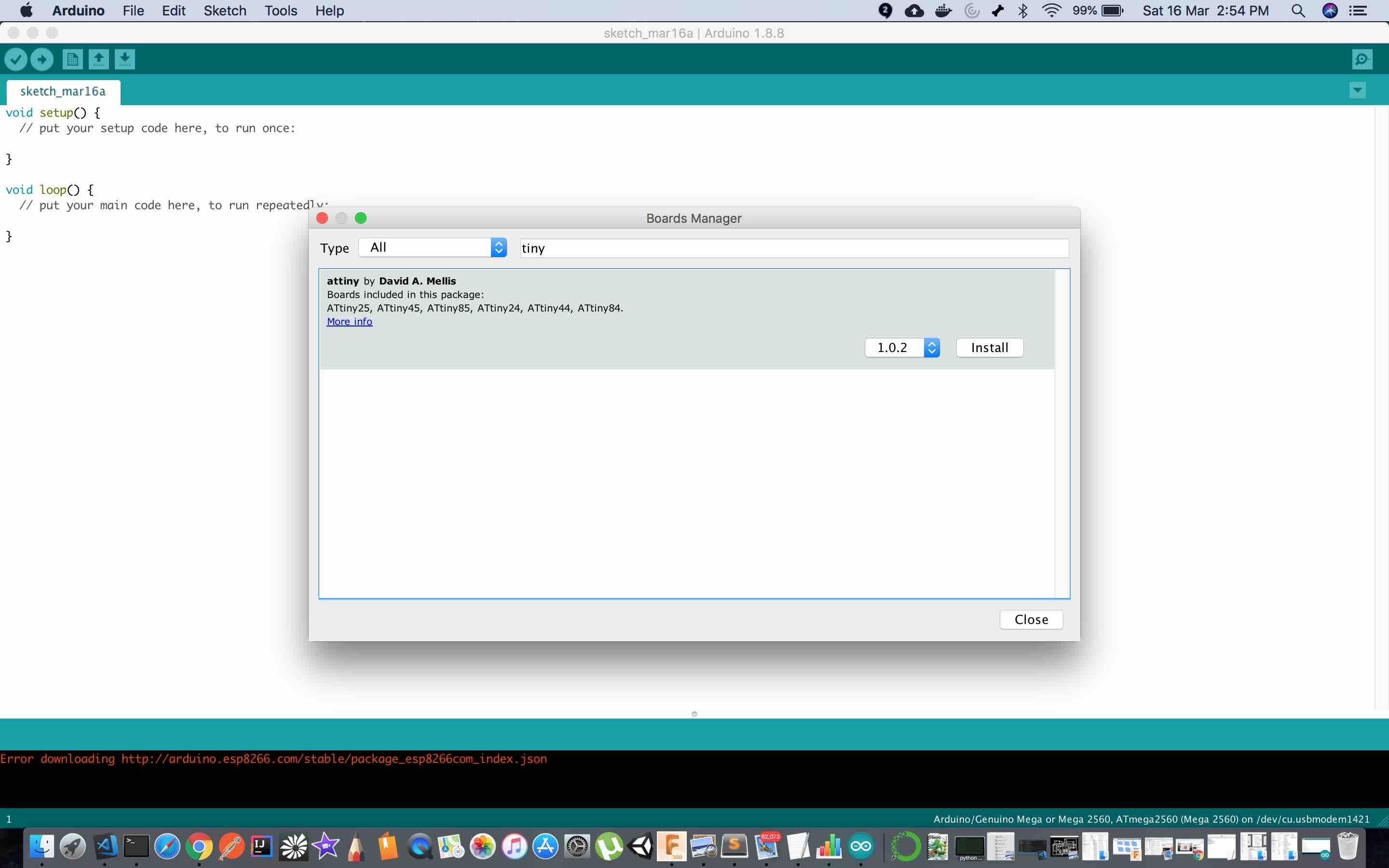
Install Additional Boards Before starting to program our board using Arduino IDE, we need to tell the software that we’ll be using a third party hardware i.e AVR ATTINY 44/45. For this we need to go to the Board Manager and add additional boards.So go to Arduino Preferences and there in the text field add a link then click ok
-
Go to the boards manager and install new board files as required
-
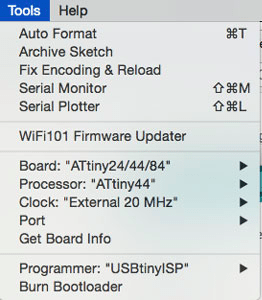
Now goto tools then to Boards and select the Microcontroller which you are using, in my case it was attiny 44 with 20Mhz external clock and programmer as USBTINY.
-
After this we need to burn the bootloader onto the chip, this step sets the fuses and flashes any previous configration over the chip.
-
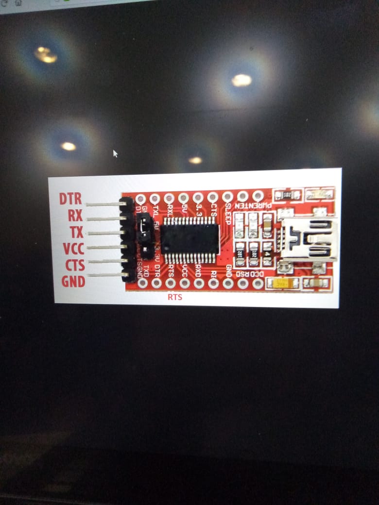
But before doing that we should always read the data sheet of the chip we are using and atleast you should know the pin diagram of the chip you are using. FTDI chip pins and how you can attach it to your board. So you need to understand the schematic too. I designed a hello board in elecronics design week. I used the Atmel AVR programmer, FTDI USB to serial convertor to program my board.
- Next step is to upload the program. I have used a sample Blink program available in arudino ide and my LED is connected to Pin2
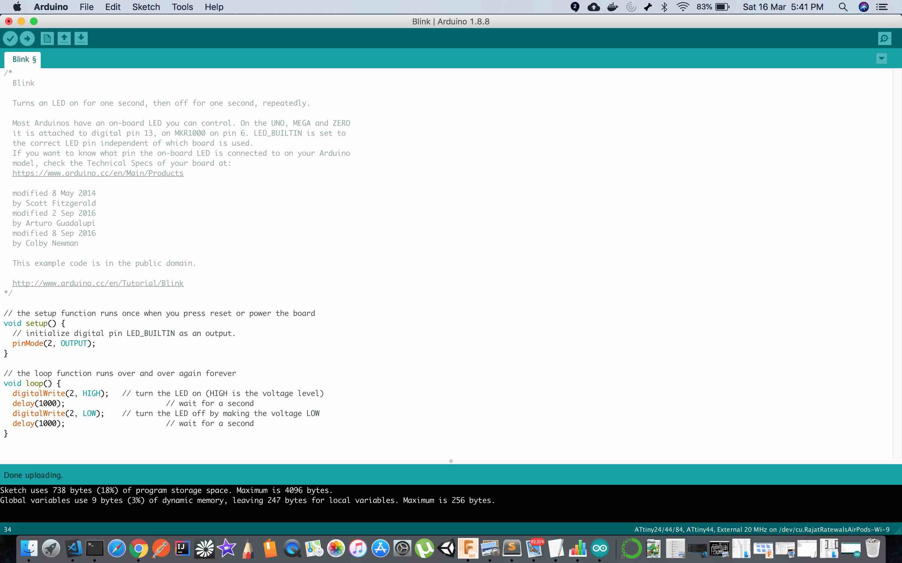
- Understanding the program, its simple actually setup initialise the output pin and Setup function runs in a loop to blink the LED
// the setup function runs once when you press reset or power the board
void setup() {
  // initialize the Output Pin.
  pinMode(2, OUTPUT);
}

// the loop function runs over and over again forever
void loop() {
  digitalWrite(2, HIGH);   // turn the LED on (HIGH is the voltage level)
  delay(1000);             // wait for a second
  digitalWrite(2, LOW);    // turn the LED off by making the voltage LOW
  delay(1000);             // wait for a second
}
Program Working Video
Group work - Embedded Programming
This weeks assignment was to Compare different Architectures of Microcontrollers.All MCs use one of two basic design models: Harvard Architecture and von-Neumann architecture
Harvard architecture
The Harvard architecture is a computer architecture with physically separate storage and signal pathways for instructions and data. The term originated from the Harvard Mark I relay-based computer, which stored instructions on punched tape (24 bits wide) and data in electro-mechanical counters. These early machines had data storage entirely contained within the central processing unit, and provided no access to the instruction storage as data. Programs needed to be loaded by an operator; the processor could not initialize itself. Today, most processors implement such separate signal pathways for performance reasons, but actually implement a modified Harvard architecture, so they can support tasks like loading a program from disk storage as data and then executing it.
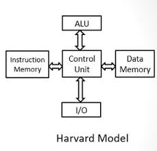
Memory
In a Harvard architecture, there is no need to make the two memories share characteristics. In particular, the word width, timing, implementation technology, and memory address structure can differ. In some systems, instructions for pre-programmed tasks can be stored in read-only memory while data memory generally requires read-write memory. In some systems, there is much more instruction memory than data memory so instruction addresses are wider than data addresses.
Applications and features of Harvard Architectures
The principal advantage of the pure Harvard architecture—simultaneous access to more than one memory system—has been reduced by modified Harvard processors using modern CPU cache systems. Relatively pure Harvard architecture machines are used mostly in applications where trade-offs, like the cost and power savings from omitting caches, outweigh the programming penalties from featuring distinct code and data address spaces. Digital signal processors (DSPs) generally execute small, highly optimized audio or video processing algorithms. They avoid caches because their behavior must be extremely reproducible. The difficulties of coping with multiple address spaces are of secondary concern to speed of execution. Consequently, some DSPs feature multiple data memories in distinct address spaces to facilitate SIMD and VLIW processing. Texas Instruments TMS320 C55x processors, for one example, feature multiple parallel data buses (two write, three read) and one instruction bus. Microcontrollers are characterized by having small amounts of program (flash memory) and data (SRAM) memory, and take advantage of the Harvard architecture to speed processing by concurrent instruction and data access. The separate storage means the program and data memories may feature different bit widths, for example using 16-bit wide instructions and 8-bit wide data. They also mean that instruction prefetch can be performed in parallel with other activities. Examples include the PIC by Microchip Technology, Inc. and the AVR by Atmel Corp (now part of Microchip Technology).
The speed aspect
A lot has been discussed about the Harvard architecture, but without the speed any architecture can’t be accepted. But in case of the Havard architecture the manufacturers have designed the architecture in such a way that it will be able to process the data with a much higher speed. Yes, all care has been taken so that the architecture can process data with a high speed.By implementing the same formula the modern days CPU are being manufactured so that the new CPU can run with a much faster sped and can also process the data effectively. The concept of the CPU cache is also being implemented while designing the Harvard architecture.
Von Neumann Architecture
The von Neumann architecture, which is also known as the von Neumann model and Princeton architecture, is a computer architecture based on the 1945 description by the mathematician and physicist John von Neumann and others in the First Draft of a Report on the EDVAC. This describes a design architecture for an electronic digital computer with parts consisting of a processing unit containing an arithmetic logic unit and processor registers; a control unit containing an instruction register and program counter; a memory to store both data and instructions; external mass storage; and input and output mechanisms. The meaning has evolved to be any stored-program computer in which an instruction fetch and a data operation cannot occur at the same time because they share a common bus. This is referred to as the von Neumann bottleneck and often limits the performance of the system.
The design of a von Neumann architecture machine is simpler than that of a Harvard architecture machine, which is also a stored-program system but has one dedicated set of address and data buses for reading data from and writing data to memory, and another set of address and data buses for instruction fetching.
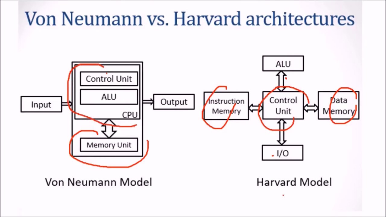
Applications and features of Von Neumann Architecture
-
The Von Neuman architecture has got extensive application in everyday life. Keeping in mind the extensive application the Von Neuman architecture has been introduced as a subject in the engendering degree. From the third semester engineering students will have the subject as their curriculum. The Von Neuman architecture consists of some important features and here we will have a detailed elaboration to the features.
-
Memory: We all know that the Von Neuman is nothing but a computer having the feature of data storage. In the architecture of the Von Neuman the memory plays a vital role and it is considered as one of the important feature. Mainly this is responsible for both holding and starting of data and programming data. In modern days this has been replaced by the RAM and now we are using RAM for this purpose.
-
Control Unit: This unit is mainly responsible for the controlling aspect. All the data stored in the memory and during the processing of data the control unit plays the role and it manages the data flow. In fact, to be more typically it is “One At A Time”. The control unit follows the principle of the One At A Time and accordingly it process all the data.
-
Input– output: Like all electronics devices the Von Neuman architecture also has an input/output architecture. It is the basic function is same and nothing specially has been designed for the input and output architecture. With the Input and output device on a person can communicate with the device.
-
ALU: ALU or the Arithmetic Logic Unit has a great importance in the Von Neuman architecture. Any sort of addition, subtraction, multiplication and division of the data will be carried out by this ALU. In addition to that any other kind of algorithmic function and activities will be carried out by the ALU. These are the basic aspect of the Von Neuman architecture which you must aware of.
Difference between Harvard and Von Neumann Architecture
Harvard Arhitecture
- The name is originated from “Harvard Mark I” a relay based old computer.
- It required two memories for their instruction and data.
- Design of Harvard architecture is complicated.
- Harvard architecture is required separate bus for instruction and data.
- Processor can complete an instruction in one cycle
- Easier to pipeline, so high performance can be achieve.
- Comparatively high cost.
Von Neumann Architecture
- It is named after the mathematician and early computer scientist John Von Neumann.
- It required only one memory for their instruction and data.
- Design of the von Neumann architecture is simple.
- Von Neumann architecture is required only one bus for instruction and data.
- Processor needs two clock cycles to complete an instruction.
- Low performance as compared to Harvard architecture.
- It is cheaper.