7. Electronics design (Mar 06)
This week we were suggested to use the test equipment to observe the operation of a microcontroller board for the group assignment. For the individual assignment, we had to redraw the echo hello world board in an electronics design software, check the design rules, make this board and test it. For extra credit, we could also simulate its operations and render it.
Designing PCBs
This was the individual assignment of redrawing the echo hello world board all the way upto making this board and testing it.
Schematic by hand
This board was to be redrawn in PCB design software.

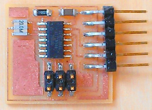
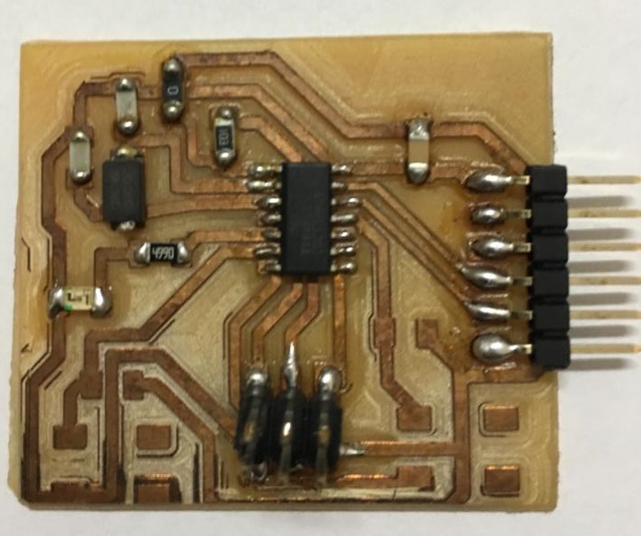
The echo hello world board after PCB milling and soldering of components.

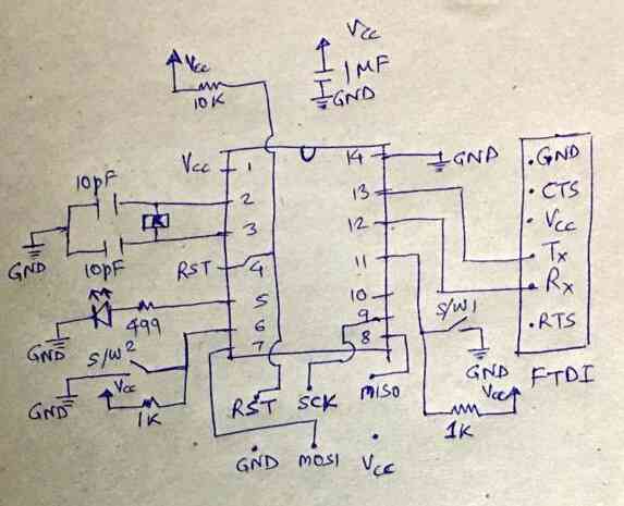
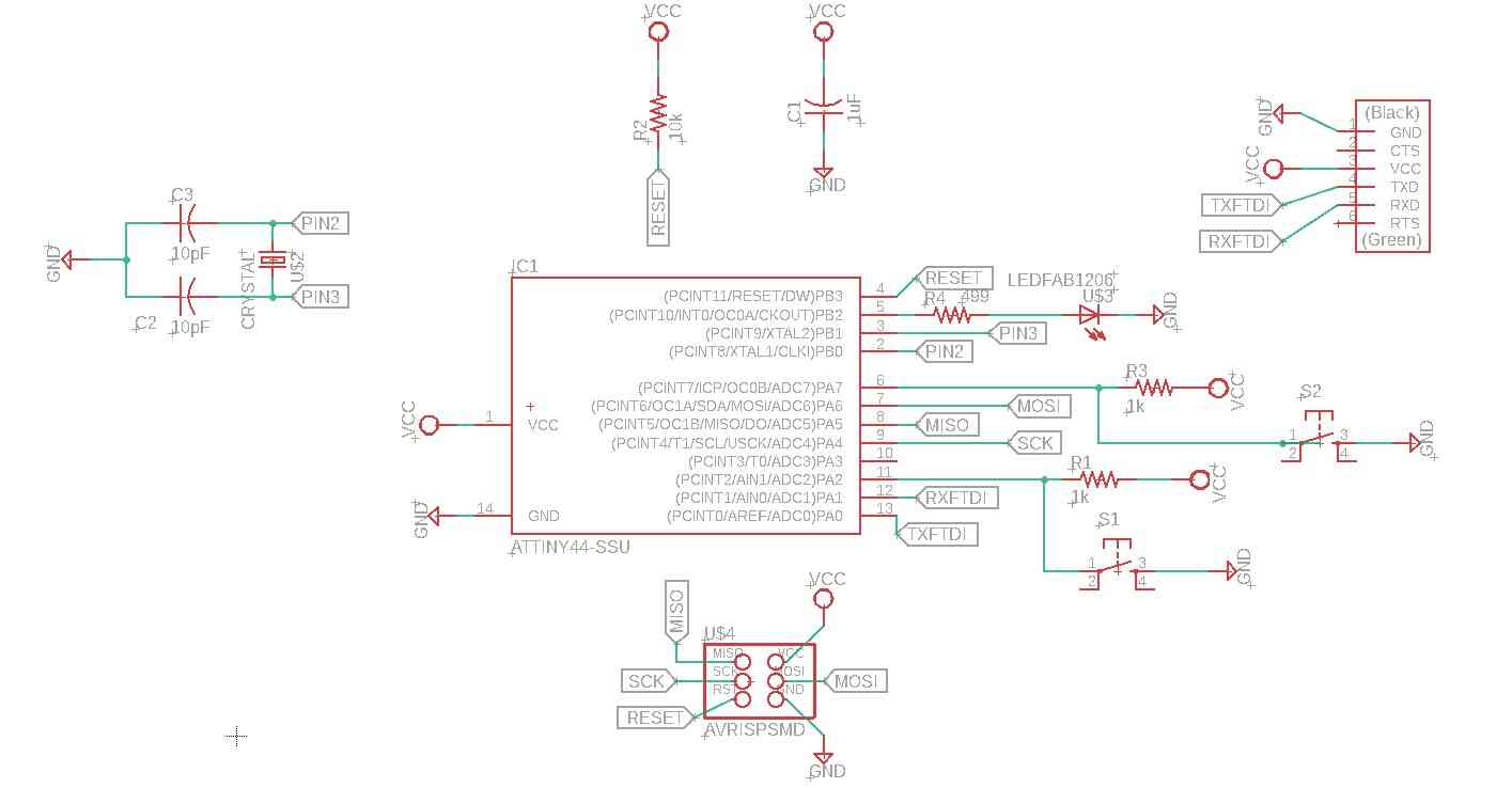
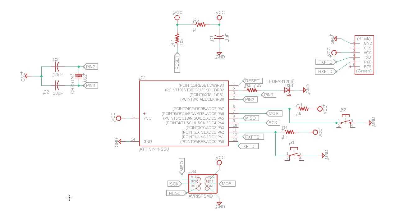
I designed the PCB schematic by hand and added a few extra components which I wanted to test.
I was ready now to create this schematic in a PCB design software. I am planning to use Eagle and KiCAD software for PCB design as both of them are freely available for students and are commonly used. The libraries for components are also pretty good. Eagle could be used for integration with Fusion 360 as both of these software are from Autodesk.
Designing PCB in Eagle
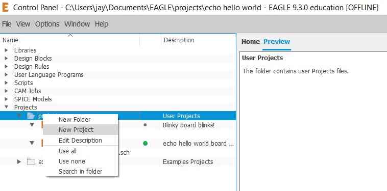
I downloaded Eagle from Autodesk website. Please open Eagle. The first screen is of the control panel. Please create a new project for the “echo hello world” PCB design.
Schematic in Eagle
I followed this tutorial for schematic design suggested by our remote instructor Puneeth Raj. The tutorial suggests to make a schematic with the components as per their specifications and footprint.
To create a schematic in Eagle, please create a new schematic in the “echo hello world” project.
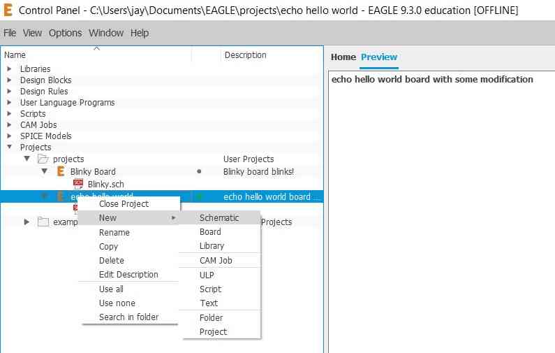
Please open the “echo-hello-world-v1.sch” schematic file created.
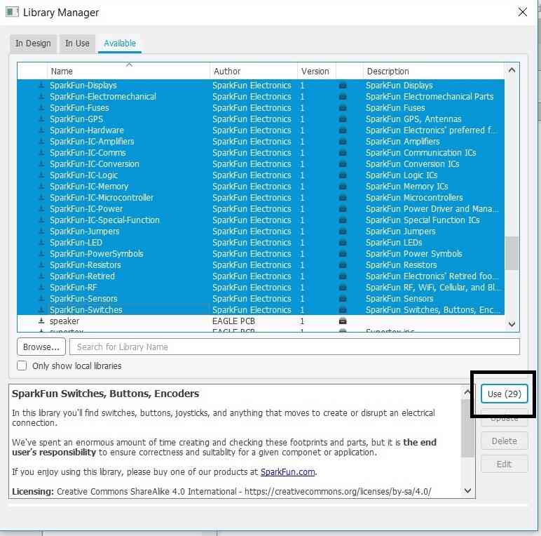
Firstly, we may want to add a library of specific parts. For instance, our regional reviewer Ohad suggested to download the Sparkfun library for the components from Sparkfun. Please unzip this library file and paste the files with lbr extension into the lbr folder which in my case was “C:\EAGLE 9.3.0\cache\lbr”. In order to be able to use these parts in the schematic, please open the library manager under the “Library” menu icon. Please click on the “Available” to know the available libraries. Please select the Sparkfun libraries that you want to download and click on “Use” to be able to use them.
These libraries would appear in the “Use” icon now.
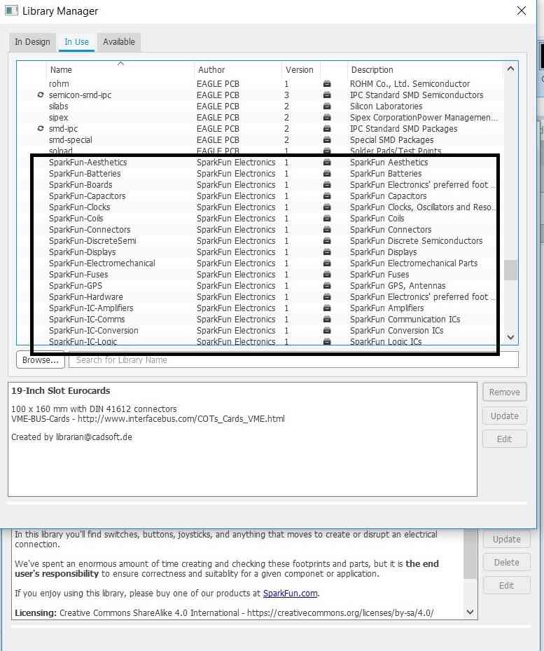
Similarly, I downloaded the Fab Library to make it easy to use the components for our PCB design and followed the same steps as for the Sparkfun libraries.
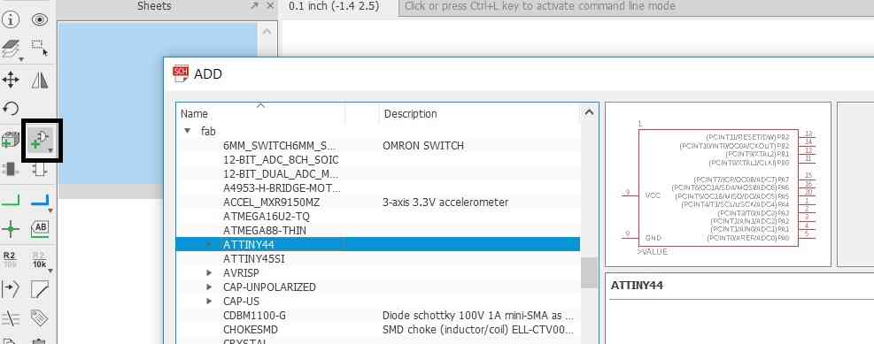
Next step was to add parts from the Fab library into our schematic. The below screenshot shows adding of ATTINY44A ssu into our schematic.
Likewise, all the other parts were added into the schematic.
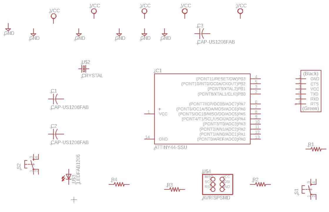
Next step was to join these parts together to create a schematic. Labels were used to join the parts to improve the clarity of reading the schematic.
PCB layout in Eagle
I followed this tutorial for PCB layout suggested by our remote instructor Puneeth Raj.
Clicking on generate/switch board button in the top left screen, next to the print icon, generated the board from this schematic.
We place the components inside the board layout with drag and drop. I have placed the components as per Neil’s echo hello world board layout.
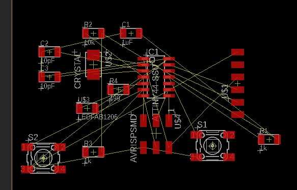
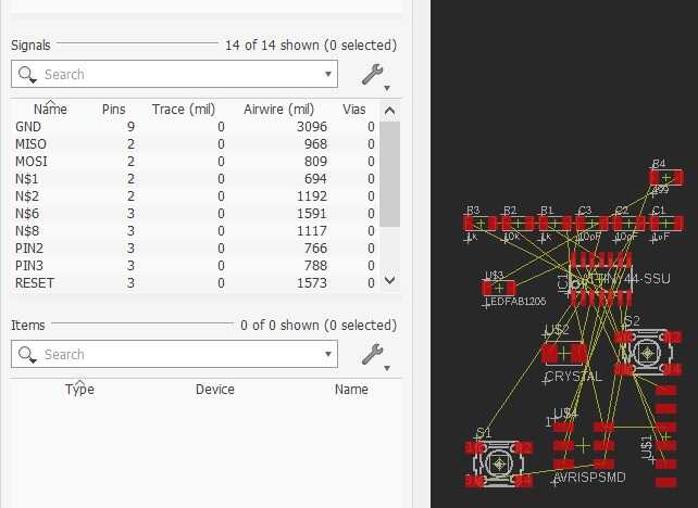
With further layout adjustments, we apply ratsnest to improve the routing.
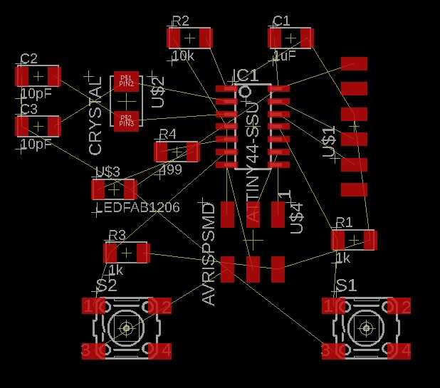
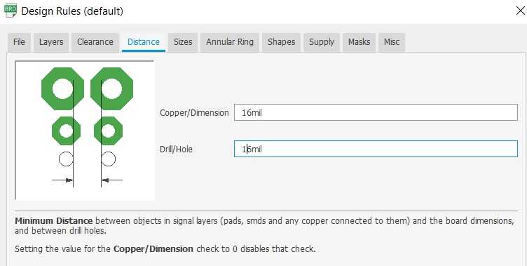
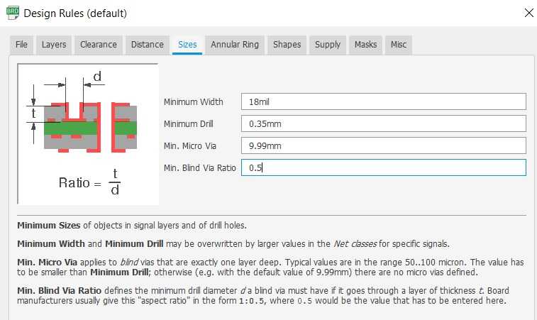
Next, we reduce the board layout boundaries and move the boundaries such that the origin is on the bottom left of one of the corners. After that, we carry out Design Rules Check to make sure that our board has the right clearance and size for the traces as per the capabilities of our tool which is 1/64 inch end mill cutter or an equivalent.
![]()
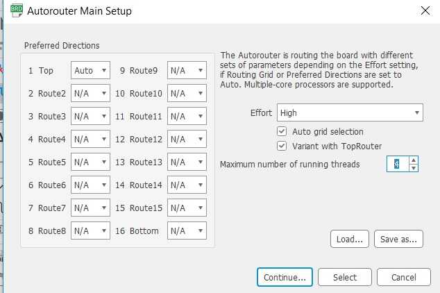
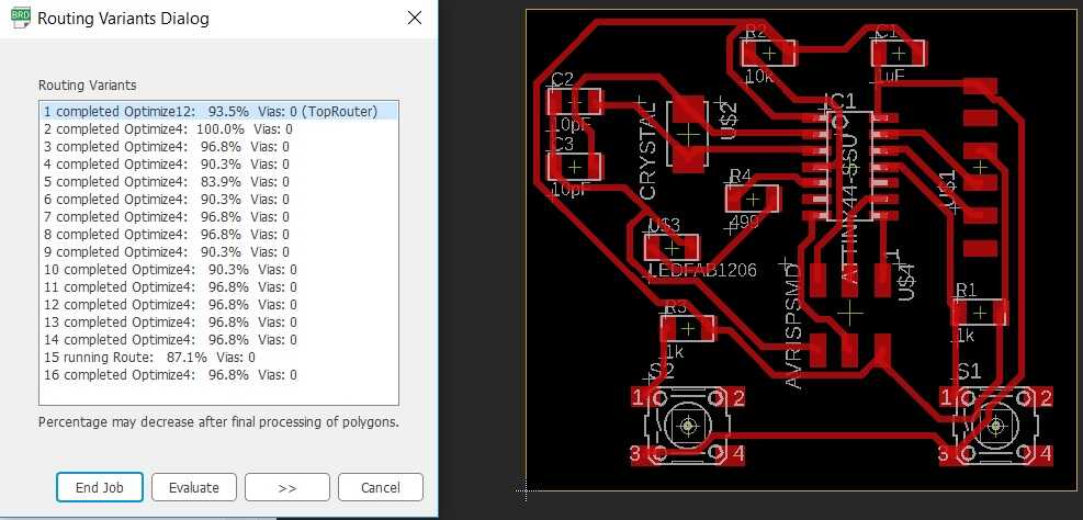
Auto router gave very good results with only two airwires which can be either manually routed or we can use external jumpers to complete the traces.
I did some manual routing to reduce the size of airwires so that I can add external jumpers i.e. 0 ohm resistors for the traces.
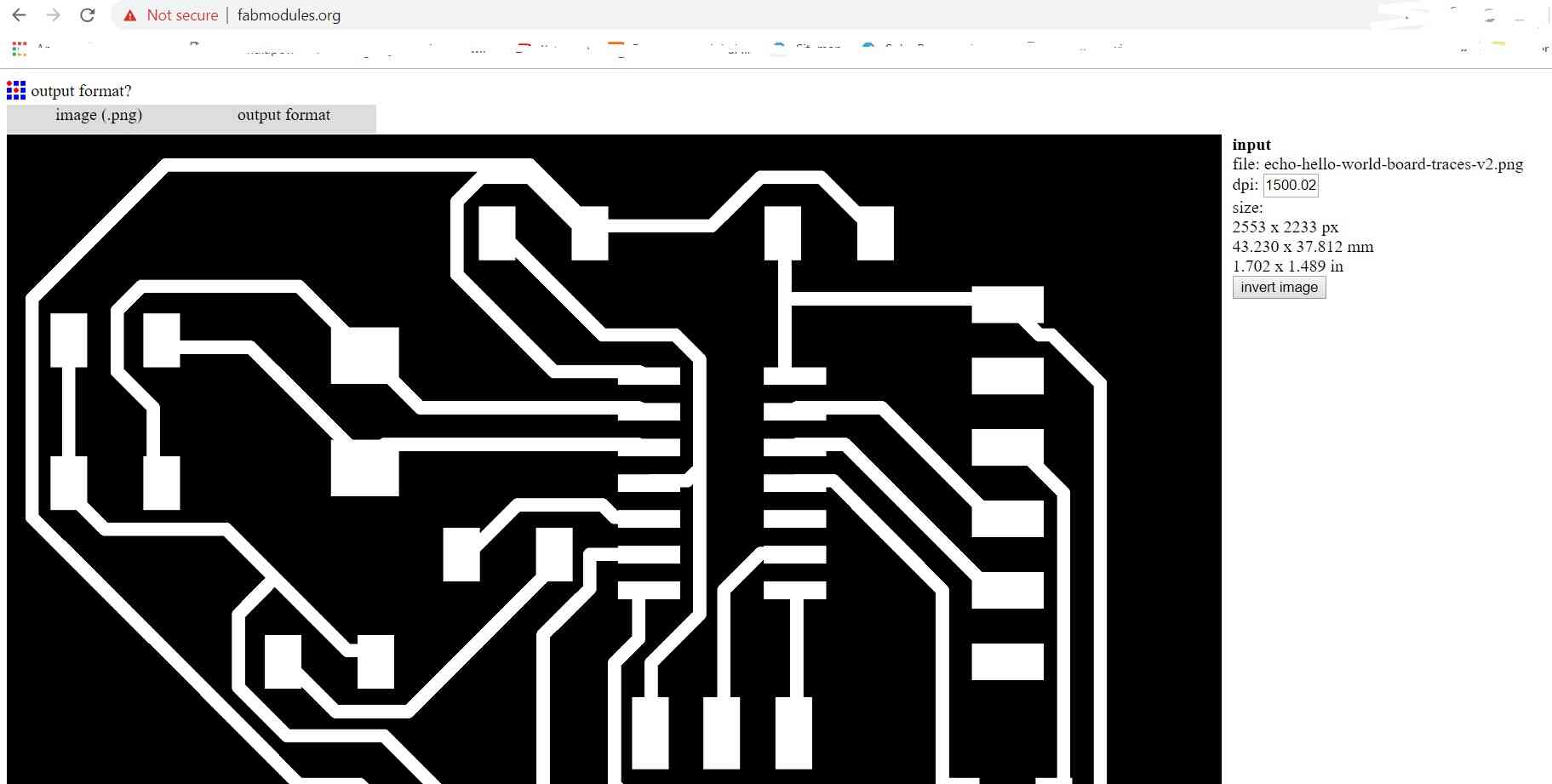
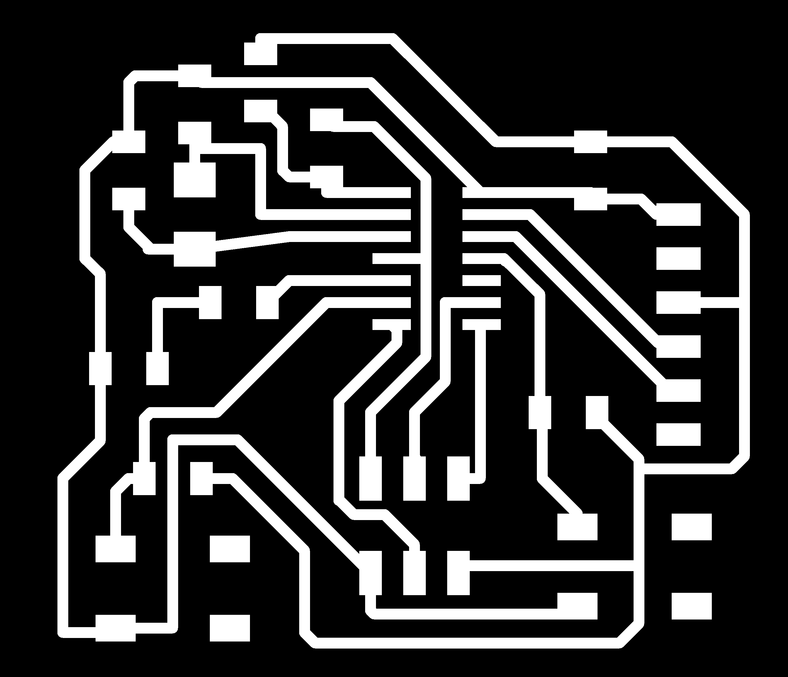
This png can be used with mods or fabmodules to convert it to rml file for srm-20 for milling the pcb.
We wanted to find out the dimension of the outline.png to cut this pcb. Reading the traces png image on fabmodules suggested an outline png size of 45 mm by 40 mm.
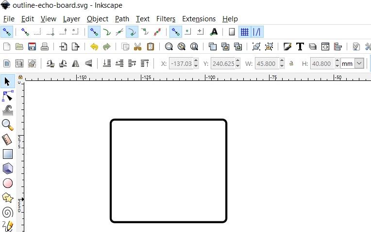
This outline was created in inkscape with a stroke width of 0.8 mm corresponding to the 1/32 inch end mill for cutting.
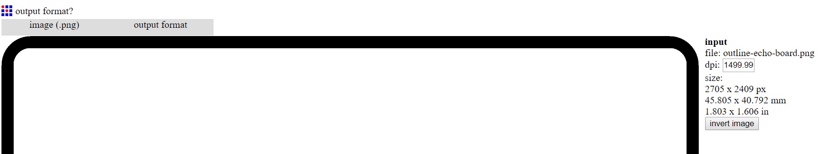
This outline’s dimensions were confirmed in fabmodules website.
The final outline.png has been shared.

Final PCB
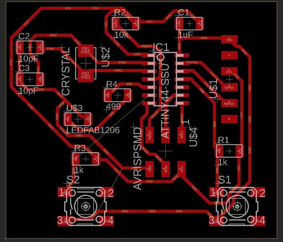
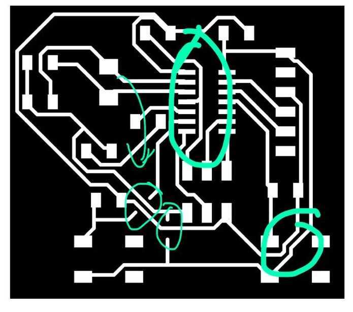
When I asked by local instructor Rahul for his feedback on my PCB design, he suggested to increase the track width and clearance and add the 0 ohm resistors as jumpers in the schematic as well. He also pointed to traces being very close to each other in the following image.
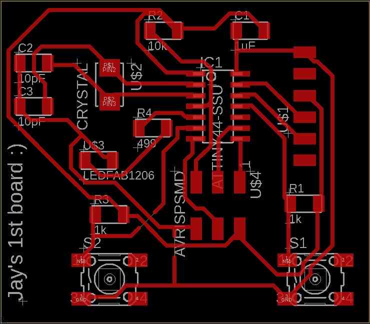
I thought of creating another PCB with his suggestions. I increased the track width and clearance to 20 mil and added the 0 ohm resistors in the schematic. I went through the entire process again. I attempted to reduce the size of the board while making sure that the traces were not too close to each other. I also did manual routing to achieve my objectives. I was able to finally remove the 2 jumpers that I was needing initially but instead I needed another jumper of 0 ohm resistor. The final schematic, the layout and the traces png are given below.
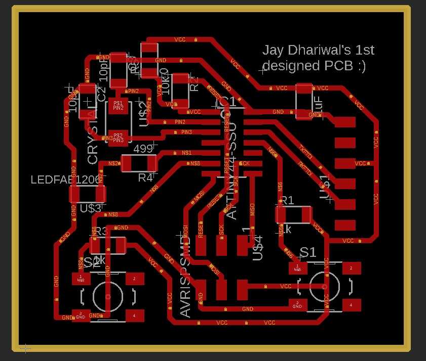
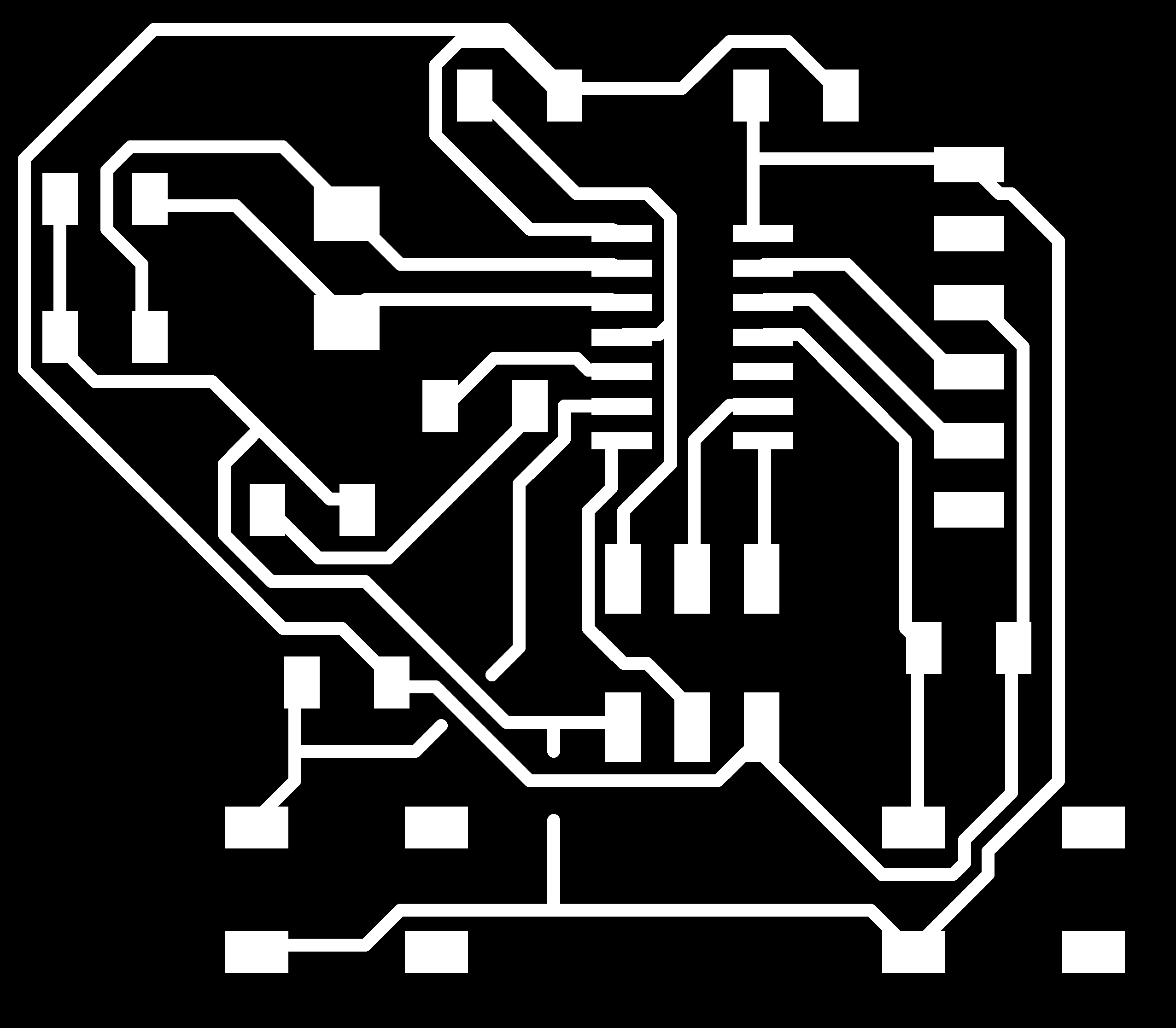
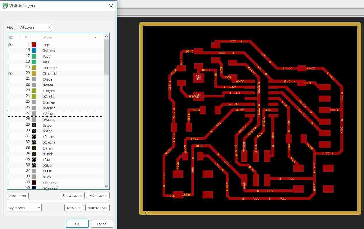
To get the png, we turn off all the layers except the ones with the traces and the outline.
We save the png as a monochrome.
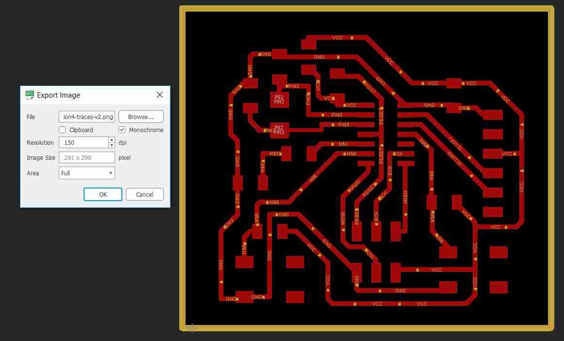
We trim the png to get the below image which could be used with fabmodules to generate an rml file.
The rml file can be downloaded.
I had some difficulty in setting up the outline file as it was not on the origin in the Eagle layout software module so I cut the outline with a knife as I was short on time. The final milled board looked like this. There were some traces which were not as clean due to my copper board not perfectly levelled. I used a cutter to remove those traces.
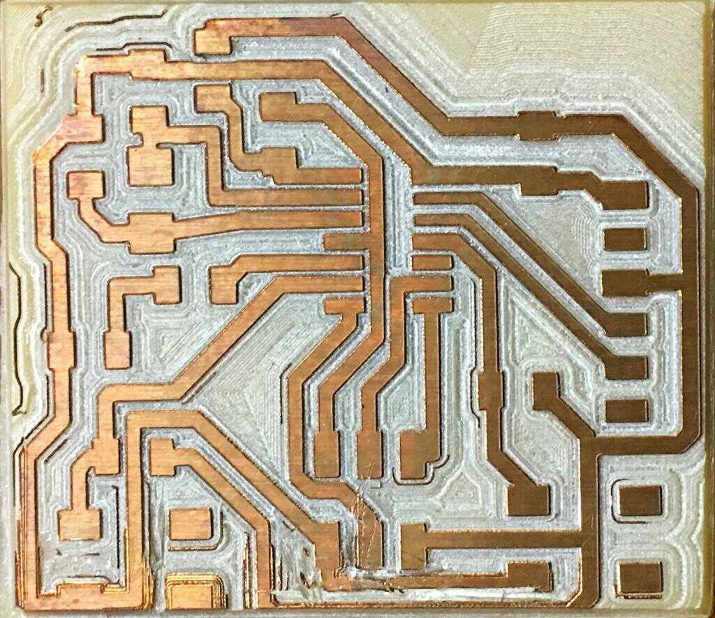
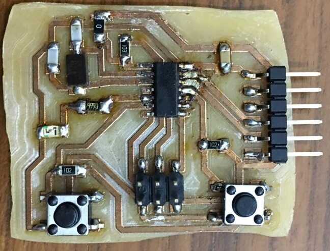
I soldered the components on it and am ready to program it.
I had then cut another board with traces with the outline to make up for the outline that I didn’t cut earlier.
I am very happy to have reached this stage and am looking forward to programming this board!
Kicad
I also tried Kicad as it was open source but I had also heard that it had a steep learning curve. I wanted to try this out as Neil had good things to say about it. I started with Kicad with these fab resources on Kicad. I started with this course on building something in Kicad as fast as possible.
I installed Kicad version 5.1.2 which was about 1 GB in size.
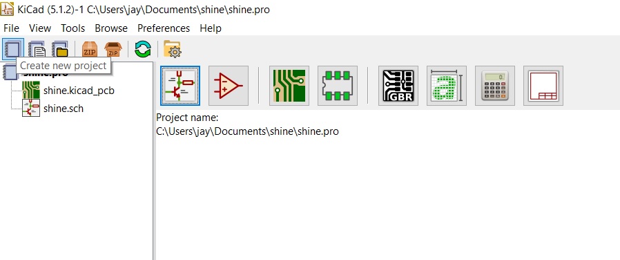
Then I opened a new project and named it shine.
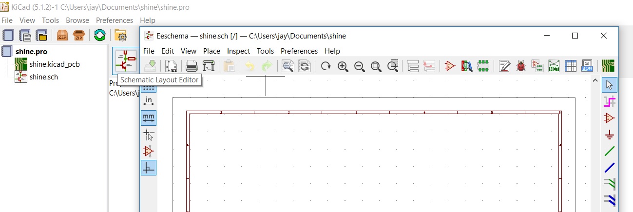
Next I opened the schematic editor.
First thing to know is the Hotkeys List which can be useful in the long run. Pressing Ctrl+F1 gets this list.
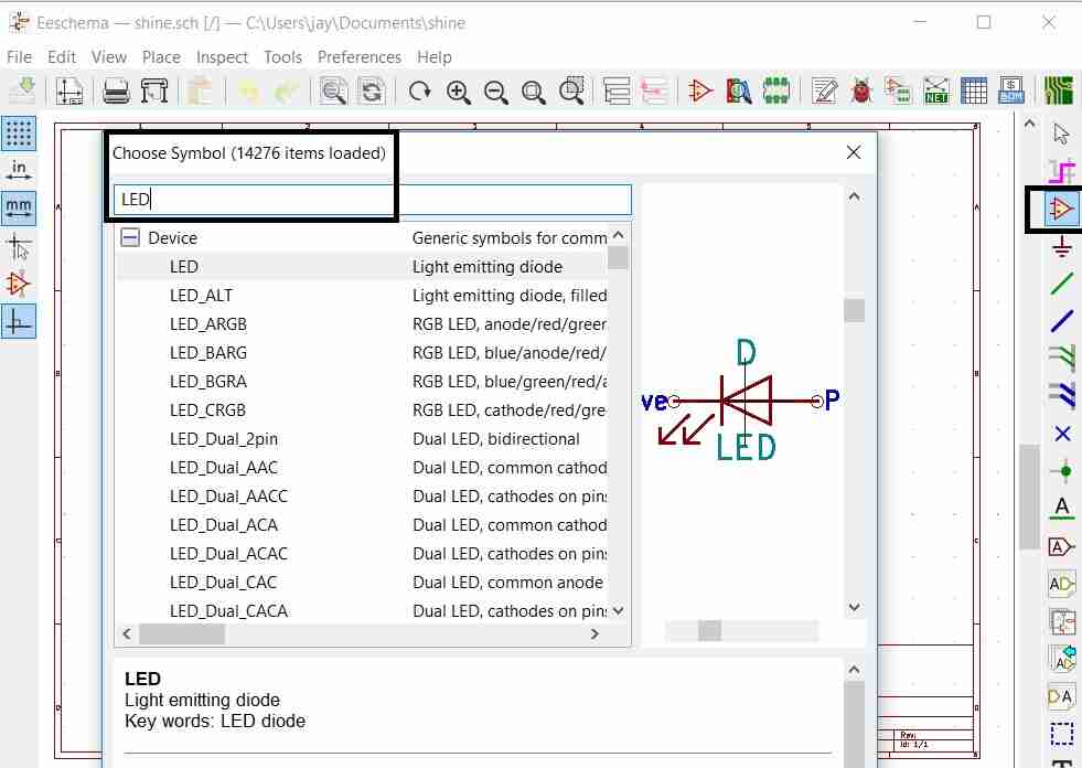
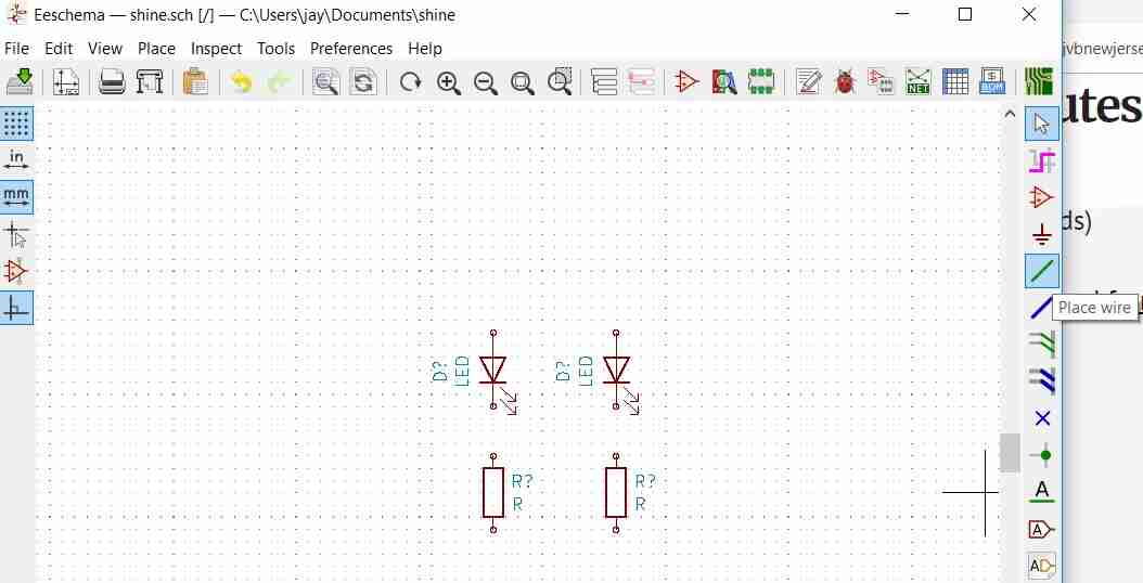
Next we start adding components to the schematic editor.
After placing a few components, we place wires to connect them.
We want to hook this PCB up with Raspberry Pi. The Raspberry Pi pin layout is given below from this link.
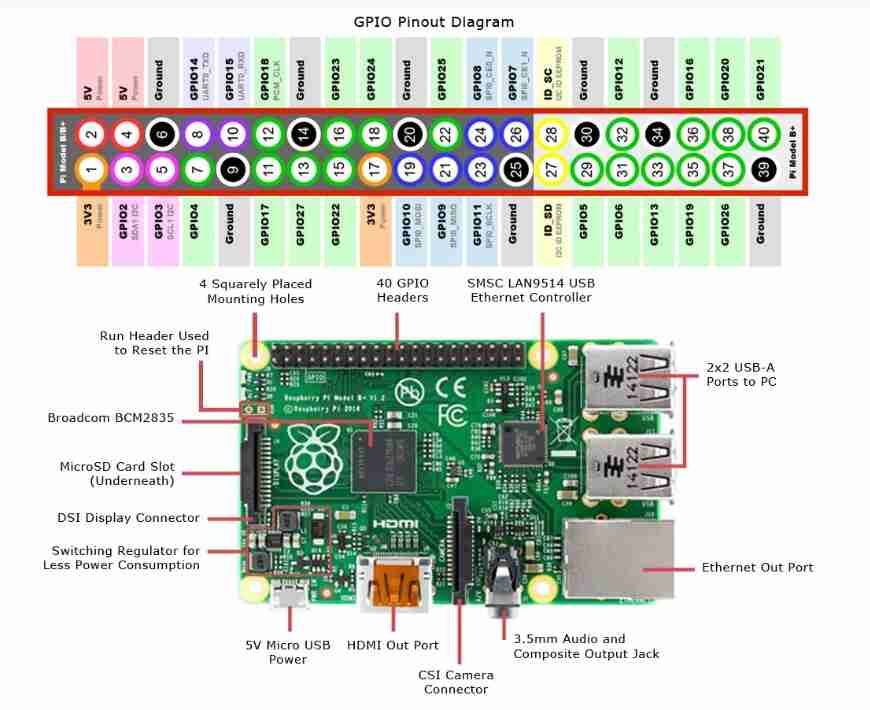
We add a 2X5 Connector in the Schematic Editor and place text as per the 1-10 pins on R Pi.
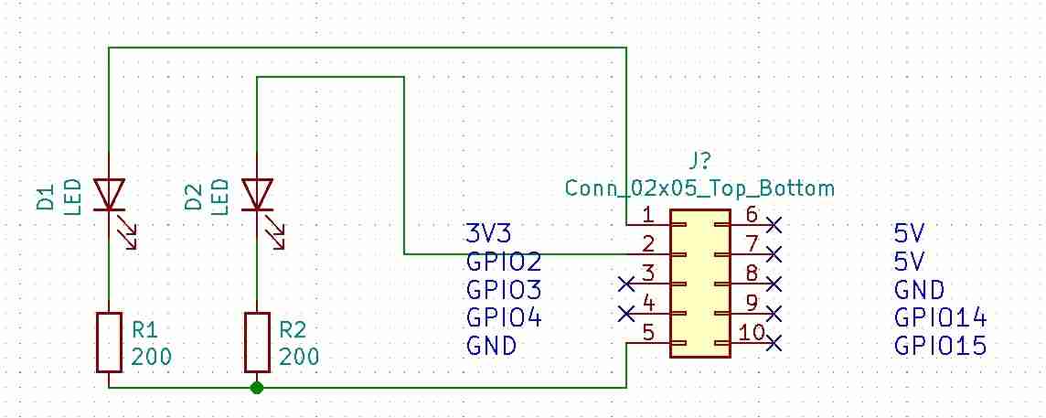
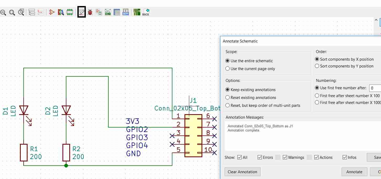
We then give value to resistors, mark the R Pins not used with an X. We then annotate all the components which removes the question mark symbol from the components.
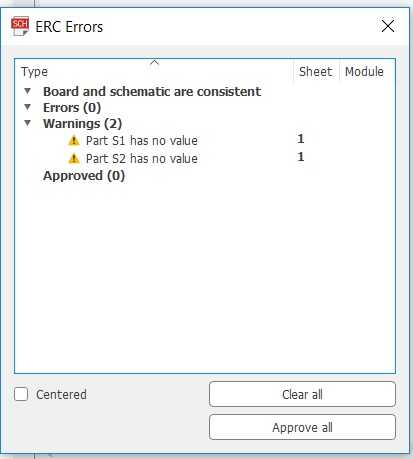
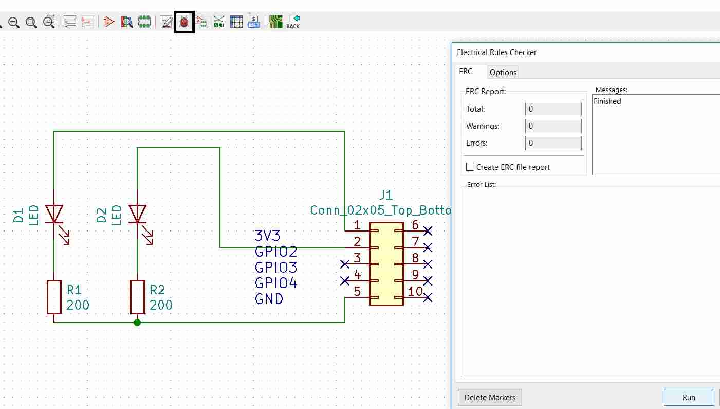
We then run the Electronic Rule Check (ERC) to make sure everything is connected alright. Once run, we don’t get any errors.
We generate a netlist which related the schematic to the layout. We then want to assign footprints to schematic symbols.
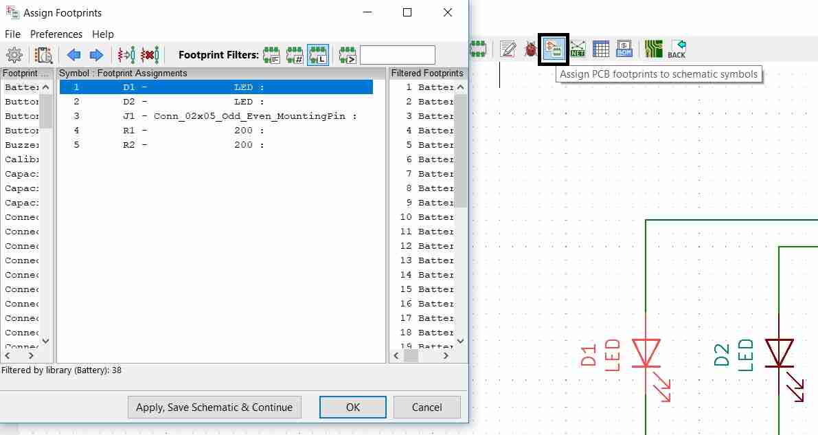
We assign the footprints to our schematic symbols of LEDs, Resistors and Connector and then save our selections.
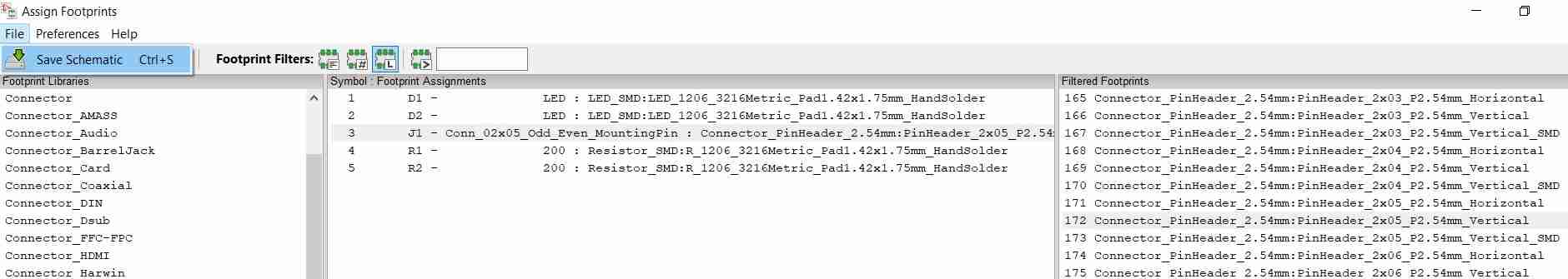
We generate the net list again as we have assigned footprints to our components now.
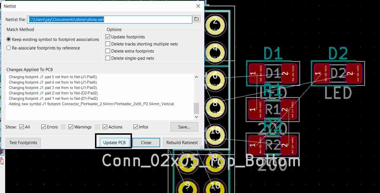
We now start the PCB layout editor to layout our PCB. We load the netlist in the PCB layout editor and update the PCB to get the components in this editor as per the image below.
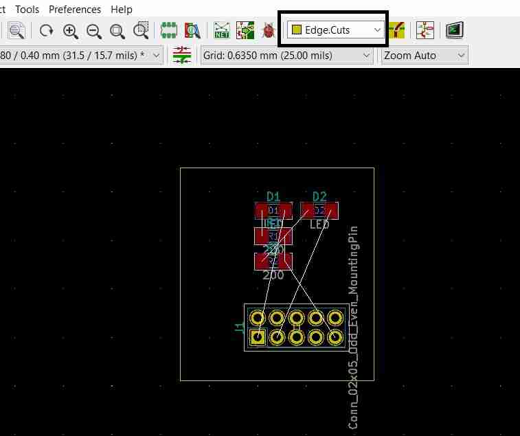
Next we move the connector to lay it out horizontally since it would be connected to R Pi pins 1-10. We then want to draw outline for this board. We select the graphic lines icon. We then select the Edge.Cuts layer for the outline. Next we bring the mouse to where we want to define the origin and hit spacebar to know the dx and dy values in the bottom bar relative to our origin. Next we change the grid size to 25 mils.
We now move around our components within the outline. Once we are happy with that, we would draw the traces on the top copper layer. The first trace is drawn between the two resistors and the ground pin 9 on the connector.
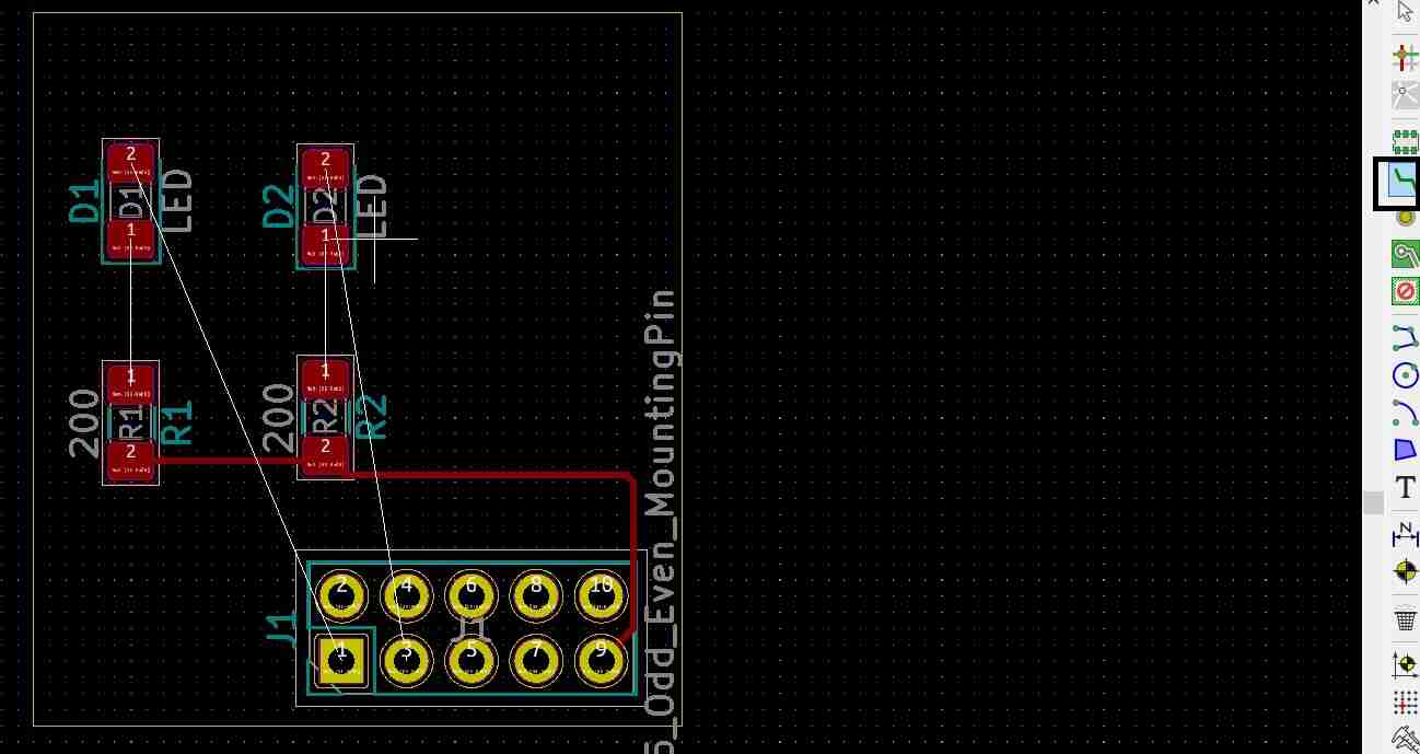
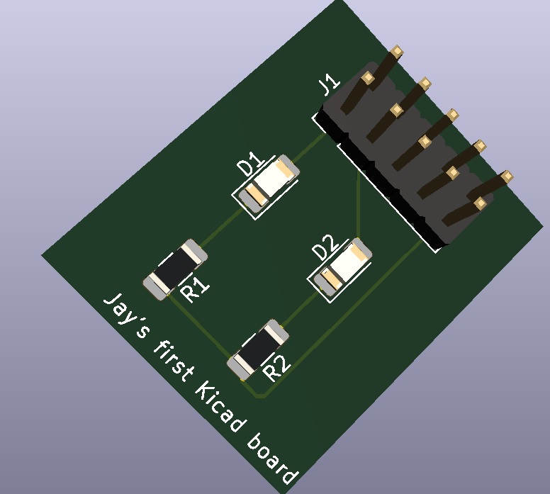
Likewise, we can connect the other traces. We can add text to our PCB with the F.silk layer. Then we can view our PCB in the 3D Viewer.
We can then export our file as an svg. We can open this svg file in Inkscape and export it as png for the traces.
Learnings from using Kicad
I would say that I was pleasantly surprised to get started with Kicad. I would like to explore it more with time. Neil had shown in this video about how to build circuits with ATTINY uC with Kicad.
For now though since Eagle has been around for quite some time and the libraries and support on the internet is more readily available so I would use Eagle for this session.
Design files
Download for the eagle project file for the echo hello world board.
Download for the eagle schematic file for the echo hello world board with auto routing only.
Download for the eagle board file for the echo hello world board with auto routing only.
Download for the eagle schematic file for the echo hello world board with manual routing also to reduce the length of air wires for ease of using the external jumpers with 0 ohm resistors.
Download for the eagle board file for the echo hello world board with manual routing also to reduce the length of air wires for ease of using the external jumpers with 0 ohm resistors.
Download for the final traces png for the echo hello world board.
Download for the inkscape file with the outline vector drawing for the echo hello world board.
Download for the outline png for the echo hello world board before corrections.
Download for the final Eagle schematic file for the echo hello world board.
Download for the final Eagle board layout for the echo hello world board.
Download for the final traces png for the echo hello world board.
Download for the Kicad board layout for an example.
Download for the Kicad schematic for an example.
Observing operation of microcontroller (Group Assignment)
First of all, I brushed up my knowledge on the electronic components. Equipment to be used are digital multimeter, dc power supply and oscilloscope, if it is available.
Digital multimeter
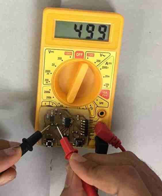
Digital multimeter is used to check continuity of the traces of the pcb, measure dc and ac voltages as well as measure resistances of resistors and diodes.
Here, I am measuring the resistance of the 499 ohm resistor in the echo hello world pcb.
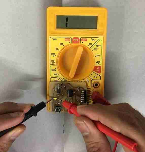
I am checking whether the LED is working or not using the multimeter.
Here, I am measuring the dc voltage of the dc power supply.
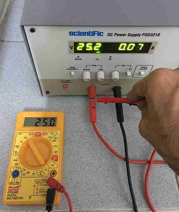
DC power supply
I have a Scientific DC power supply PSD3210 in my office. It is a single channel variable DC power supply with DC voltage ranging from 0-32V and current from 0-10 A.
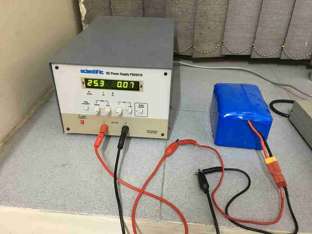
I have used this in my project to charge the 11000 mAh lithium ion battery of my e-bike conversion kit.
Digital Storage Oscilloscope
We didn’t have a DSO at this point. I have shown it in input devices week and provided a link.

Solar powered electric bike con kit by Jay Dhariwal is licensed under a Creative Commons Attribution 4.0 International License