5. Electronics production (Feb 20)
This week we were suggested to characterize the design rules for PCB production process for the group assignment. For the individual assignment, we had to make an in-circuit programmer by milling the PCB, program it and then, optionally, trying other processes.
Characterization of design processes for PCB production (Group Assignment)
This is all new stuff for me so in the spirit of spiral development, I wanted to do the bare minimum first and then proceed to do more things, which I was very excited about.
Fabmodules file prep
I had used the png of traces and instructions from Brian’s FabISP webpage.
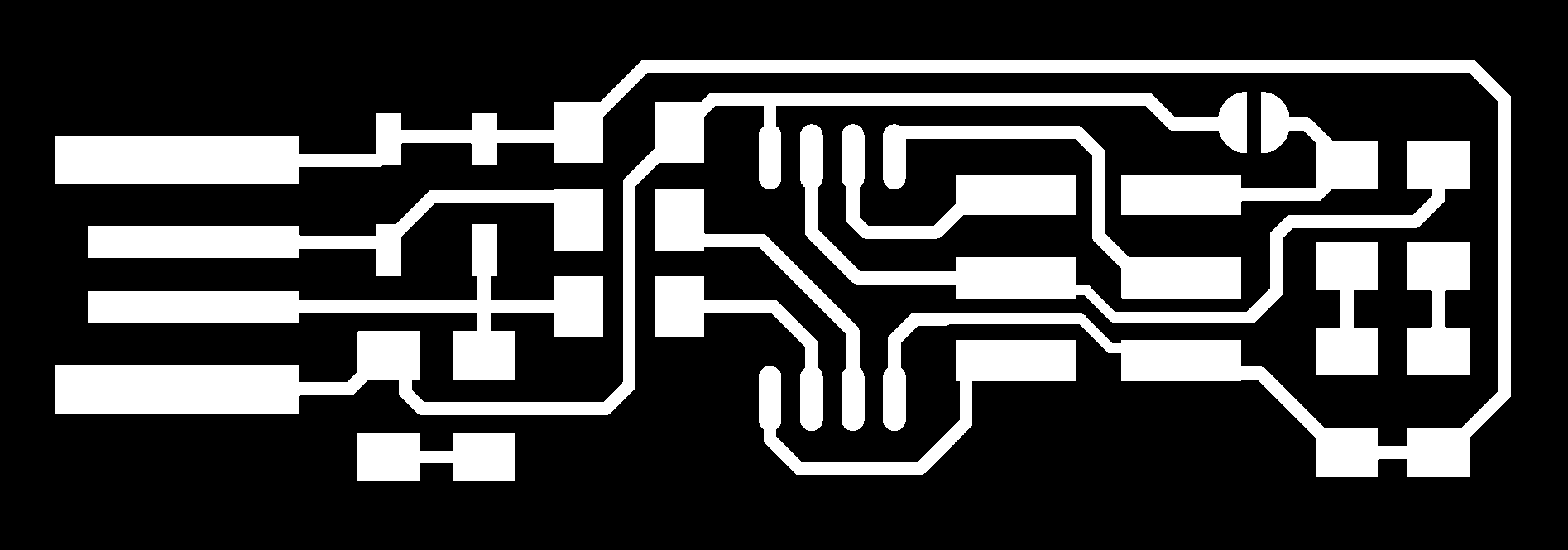
I used fab modules for converting this png image to rml file readable by Roland SRM-20 machine. The below images show the steps taken for creating a traces rml with the settings for a V bit.
First, we select the input image to be png and load it onto the screen. Then, we select the output image type to be of extension rml as we use Roland SRM-20 for pcb milling which uses this file format.

We select the process to be PCB traces (1/64) as either we use 1/64 inch end mill or we use V-bit with which we adjust the parameters for this process for milling PCBs.

When the process is selected to be PCB traces (1/64), we get the screen as per the image below to select the process parameters, then calculate the tool path and then save the file as an rml file to be fed to Roland SRM-20.
The cut depth parameter is the total depth that the tool should go into the workpiece for milling. Since the FR-1 copper boards have a depth of 0.07 mm so slightly more than that is appropriate.
The tool diameter is the diameter of the tool used. In our case, we used a V-bit. Since we want to limit the trace width to 0.4 mm so the maximum tool width should be in this range of 0.35 to 0.4 mm. Since the angle of our bit is 60 degrees so we are safe.

The other parameter is the number of offsets. This is the number of times the same copper is milled with some offset to make sure that no part of the trace is left. We can also use -1 to have the offset to a very high value. This is the best but takes a long time.

This shows the tool path achieved with the above parameters.

The rml file created from the fab modules interface have to be fed to the Roland SRM-20 software Vpanel for milling.
Surfacing
We need to make sure that the bed of the machine is levelled before we can use it. Surfacing is the process which is used to level the bed. If the bed is not levelled, it can lead to poor trace creation.

This assignment was a part of group work and was done with our local instructor Rahul. The Clickmill software was used. The material for the sacrificial layer over the bed is selected. It is either acrylic or wood.

A pocket is defined to be cut.

The bit of 4 mm is selected for pocketing.

This is the bed that was used after surfacing. We can check if the bed is levelled with a mobile app. We need to place the copper FR1 board with double sided tape on this sacrifical layer.

Roland SRM-20 software Vpanel
We used Roland SRM-20 for pcb milling.

To work with SRM-20, first of all, the power button on the SRM-20 needs to be switched on.
Once the board is fixed on the bed, we need to set the origin before we start milling. The interface is very well made. The up, down, left and right buttons on the left side of the image can be clicked to move the cnc mill in x, y and z directions. We can take the tool to the appropriate origin position. The origin can be set on the right hand side of the SRM-20 interface. The view option on the interface brings the table towards the front for the user to view the part. The ‘To Origin’ option brings the tool to origin from its present position. You can see the values of x, y and z change with reference to the origin.

For the files provided from outside like ours, we need to select this option using the Setup in the previous GUI screen. The settings that we used are shown in the image below.

Here, we need to click on the Cut option in the first GUI screen. We delete all the previous files and select the rml file to be used for cutting. Once done, we click on Output to start milling.

Milling cutter precision
Using this png shared on the Fab Academy 2019 schedule page, we wanted to test how fine the traces could be cut with our milling cutters.

This was the outline for the previous traces png.

This is how the demo turned out to be with the 1/64 end mill cutter.

We had only one 1/64 end mill cutter for this week. Other 1/64 bits have been ordered but are yet to arrive. We also had V bits which we had more stock of. Ahmad Ali from our group had already done this assignment with 1/64 end mill cutter. The image shows that the cuts were very precise for the thinnest of the lines tested.

Fab ISP for individual assignment
To make FabISP. I used Brian’s board for my first ISP.
I downloaded the schematic and layout png files from his page for traces and outline cut as per the images below.


PCB milling
This image shows the cutting taking place.

This image shows the final image with the cut. The traces were not cut efficiently on one side, suggesting that the bed wasn’t levelled properly.

Difficulties faced in milling
The bed wasn’t levelled properly, which needed to be worked on. I was also not able to cut the outline completely to take the pcb out of the FR1 board. The CNC mill was making cuts in the air, probably because it was hitting the limits of cutting. I worked on resolving these issues. This was resolved in the group assignments.
Soldering
I wanted to practice soldering with smd components while I resolved the other issues with copper traces. The below images show the lens and soldering station that we had. The lens is useful to magnify the image while soldering. This helps with the smaller smd components. I like to look into the lens while soldering.

The soldering station can be used to set the appropriate temperature to solder.

These images show my attempts at soldering. I wanted to get better at it before I soldered the rightly milled boards.


The soldering technique that worked best with me was to apply the soldering paste on the pads first. Then place the smd component. The smd component would get secured in place due to the sticky soldering paste. We could use the tweezer to further secure the smd component in place. Then we need to apply the soldering iron gently with the soldering wire to solder the area in between the smd component and the pad.
I also ordered finer soldering tips and a thinner soldering wire which could help novices like me to solder without making errors.
Multimeter testing
I used a digital multimeter for thoroughly making sure that no traces were shorted where they were not supposed to be. I also tested if the resistors were connected properly.

I also checked for led connections.

Programming ATTINY44A with breadboard
While I was making the PCB with the right traces, I worked on programming the ATTINY microcontroller using Arduino as ISP. I had an ATTINY44A and Arduino Mega 2560 with me. I used this tutorial to program ATTINY44A on a breadboard and ran the blink LED program written in Arduino IDE.

The use of Arduino as ISP has been documented by me here.
Installing AVR toolchain for Windows
I have also installed the toolchain for Windows following these instructions. For the Atmel AVR Toolchain for Windows, I have installed AVR 8-bit Toolchain v3.62 – Windows from this link.
Fab ISP try for next week of 20-27 Feb
I still used the V-bit with an angle of 60 degrees for PCB milling with a shank diameter of 3.175 mm. V-bits are much cheaper than the square end mills and also less vulnerable to breakage to level differences.
This time I also used a sacrificial layer of an inverted pcb over the acrylic on the bed as suggested by our remote instructor Puneeth. We also used transparent thin double sided tape this time.


The only difference in the settings used for the parameters was for the offset to be -1. I also increased z depth by 0.05 mm or so at a time if the traces were not cut fully or if my V-bit was grazing the surface. One also needs to make sure that the V-bit has been tighetened enough for it not to move into the collet with pressure.

The traces look clean but the depth is more than it should have been. Next time, I would attempt to reduce the depth of cut for the traces.

The outline was cut keeping the tool diameter of 1 mm using the same V-bit. The stock thickness is 1.7 mm for the copper FR1 board.

I soldered the components using a micro soldering iron and solder rosincore wire of diameter 0.4 mm. I also applied solder flux paste on the attiny45 and header pins before applying the solder. I checked all the components with the multimeter after soldering to make sure that the connection was there.
Transistors instead of Zeners
I didn’t have the right zener diode so I had to slant them to reach the copper traces. My local instructor told me that what I was thinking of as zener diodes were actually transistors.


I was able to get the red LED to power on when the Fab ISP was given power from the laptop. I used the male female USB cable for that.

I still need to program this fab ISP but I don’t have access to a programmer so I would either use Arduino as an ISP or wait to go to the FabLab.
Programming the Fab ISP successfully
I replaced the transistors that I had put instead of zener diodes. I also put in more solder to improve the USB connector so that it securely sits in the usb slot.

It was time to program the fabisp now. I put a zero ohm resistor for the J1 jumper as per the Brian’s FabISP layout at the very top of this page to program the fabisp. This jumper has to be removed only after the fabisp has been programmed.
Download the firmware
I downloaded the firmware as per the link on Brian’s page and unzipped it. I opened the terminal window and cd into the source directory.

Programming the ATtiny
We need to run “make” on the terminal prompt to build a hex file which would be programmed onto ATTINY45. After the command completes we should have “fts_ firmware.hex” file in this directory.

Next we need to edit the makefile in a editor such as Sublime Text for the programmer.

We need to search for this text string:
PROGRAMMER ?= usbtiny
Change it to the programmer that we have. If we are using another FabISP to program this FabISP then we don’t need to change it. But if the programmer is different such as AVR ISP MKII. In that case, we need to change this line as:
PROGRAMMER ?= avrispmkii

I installed Zadig and then used it to install the drivers for avrisp mkii and usbtinyspi. In Zadig, I installed libusb32 files for both these programmers.
Next we need to connect the FabISP to USB port. We were recommended to buy a USB2.0 male to female cable by our remote instructor Puneeth. The red LED lights up.
Next we need to connect the programmer via the header. Make sure that it is connected in the right orientation.

Need to run make flash. This command erases the target chip and programs its flash memory with the contents of the hex file that was built before.

Please keep in mind to start afresh in case of errors, use the command “make clean”. Now, its time to configure the fuses.
Run “make fuses”. This will set up all the fuses except the one that disables the reset pin.

Now we need to make sure that the USB works before blowing the fuse which will turn it into a programmer to program other boards but it won’t be able to be programmed itself. We need to unplug the board from USB port and also, disconnect the programmer from the FabISP as well as the computer. Then we need to plug the FabISP back into the USB slot of the computer. The FabISP should get detected in the Device Manager in Windows.
Now, we are all set to run “make rstdisbl”. This makes our FabISP as a programmer.

Once our FabISP has become a programmer, we need to remove the bridge for the jumper J1.
I had used two programmers for programming my programmer, AVR ISP MKII and Ahmad Ali’s FabISP up until the very last steps of making the fuses when the process becomes irreversible.
Summary of programming FabISP
This was quite an experience since I had never done this. Especially, when things didn’t work to begin with, be it with the levelling of SRM-20 issue to finding the right components to using a programmer. But at last it all came together.
I first programmed ATTiny44 with an Arduino as an ISP on a breadboard. This provided some confidence of using other programmers as ISPs.
I used two ISPs to program my FabISP i.e. AVR ISP MKII and another programmed FabISP. The procedure was to install AVR toolchain for Windows and drivers for the programmers, download the firmware, make hex files to be loaded into the FabISP, flash the firmware onto the FabISP using the programmer with SPI communication protocol and set fuses. Then we find out if the programmer is detected as a device in Device Manager and then we run “make rstdisbl” to finally make FabISP a programmer.
Design Files
Download for the rml file for Roland SRM-20 with information about traces for Brian’s FabISP.
Download for the rml file for Roland SRM-20 with information about the outline cut for Brian’s FabISP.
Download for the code for arduino as isp.
Download for the blink program that I have used with ATTINY44A.
Download for the settings for traces with offset of -1 for Brian’s FabISP.
Download for the rml file for Roland SRM-20 for traces with offset of -1 for Brian’s FabISP.
Download for the settings for the outline with diameter of 1 mm for Brian’s FabISP.
Download for the rml file for Roland SRM-20 for outline with diameter of 1 mm for Brian’s FabISP.
Download for the rml file for Roland SRM-20 for outline with diameter of 2 mm for Brian’s FabISP.

Solar powered electric bike con kit by Jay Dhariwal is licensed under a Creative Commons Attribution 4.0 International License