Electronic Design
- 1. Redesign a Hello Board and add at least one LED and BUTTON
- 2. Group test about how board are get signal
- 3. Testing the program
Electronic Design
I have little bit knowledge about electronics, after that more information i search in Google to got knowledge about electronic symbol, different parts their uses, how i denoted them in design etc.
Electronic Basic:
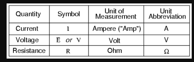
Current- I: Current is a flow of electrical charge, usually electrons or electron-deficient atoms.
Volt/Voltage-V: A quantitative expression of the potential difference in charge between two points in an electrical field, for example a battery. The greater the voltage, the greater the flow of electrical current.
Ampere-A: An ampere is a unit of measure of the rate of electro flow current in an electrical conductor.
Watt-W: It is used to specify the rate at which electrical energy is dissipated or the rate at which electromagnetic energy is radiated, absorbed, or dissipated.
Capacitor-C: A capacitor is a passive electronic component that stores energy in the form of an electrostatic field.
Resistor: A resistor is an electrical component that limits or regulates the flow of electrical current an electronic circuit. Resistors can also be used to provide a specific voltage for an active device such as a transistor.
Ground-GND A ground is a direct electrical connection to the earth, a connection to a particular point in an electrical or electronic circuit.
Positive-VCC VCC stands for "voltage at the common collector." The letter "V" on a circuit stands for the supply voltage. The letters "CC" indicate that the supply voltage is positive or negative. If the charge is positive, its circuit is a Negative-Positive-Negative circuit, and if negative, it is a Positive-Negative-Positive circuit.
Diode: HA diode is a specialized electronic component with two electrodes called the anode and the cathode. The fundamental property of a diode is its tendency to conduct electric current in only one direction.
LED: A light-emitting diode (LED) is a semi-conductor device that emits visible light when an electric current passes through it. The light is not particularly bright, but in most LED's it is monochromatic, occurring at a single wavelength.
Battery: Batteries are a collection of one or more cells whose chemical reactions create a flow of electrons in a circuit. All batteries are made up of three basic components: an anode (the ‘-’ side), a cathode (the ‘+’ side), and some kind of electrolyte (a substance that chemically reacts with the anode and cathode).
Useful Equation:A useful thing to remember which will come in handy when having to calculate the components, to be put on a circuit, is the following equation: R=V/I or I= V/R or V=R*I
Note:After Completing my basic electronic lesson, I started to learn about how to design electronic circuit by eagle,(a cad design software). I learned eagle basic watching a tutorial in Youtube. Here click for tutorial.. Before starting my schematic design I follow some previous student assignment how they done their design. Then i fix up my board design how is made.
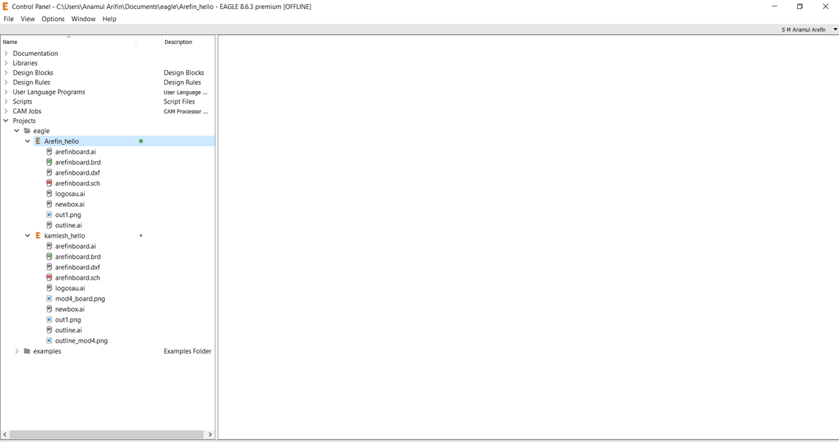
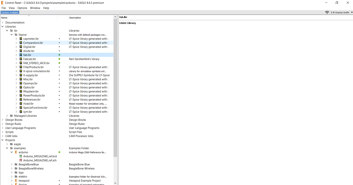
Schematic Design: First i download the eagle software from the Autodesk portal and registered as a student account. After opened the software i made a project and then upload the fab library which was i downloaded from the fab academany git repository.
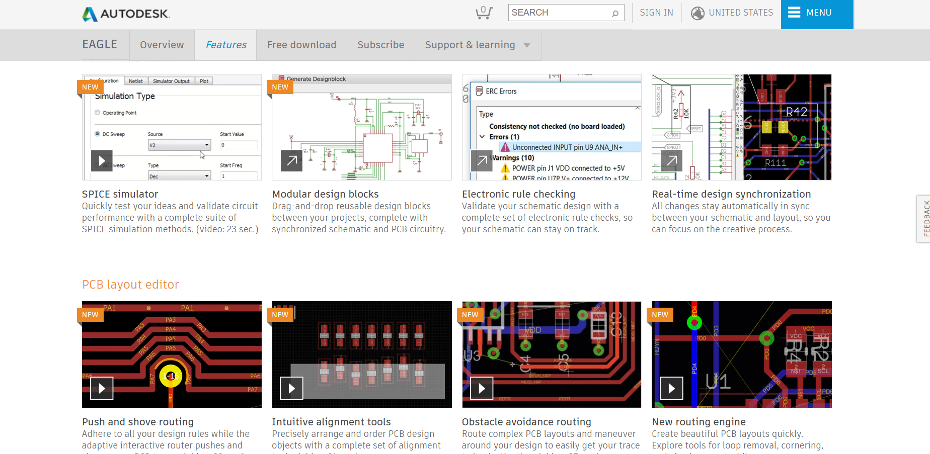
For Convenient schematic design with hits and easy to transfer it in board i choose eagle. Here some feature about eagle
For download the software go this link Click here for download
Components:
According to the design i choose all component from the fab library to design hello board schematic design. Adding all component i used name and label attribute to connect or netting the one component other component. Bu following this process i complete my hello board schematic design.
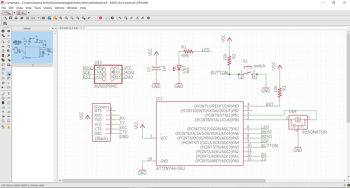
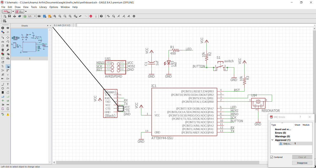
After completing schematic design i check the ER for my board design, in checking process here shows some error like, some pin of FTDI are not connect with non of the component, cause there is uses that pin. Same as from the Attiny44 where two pin still unused after adding led and button that is also detected by ERC.
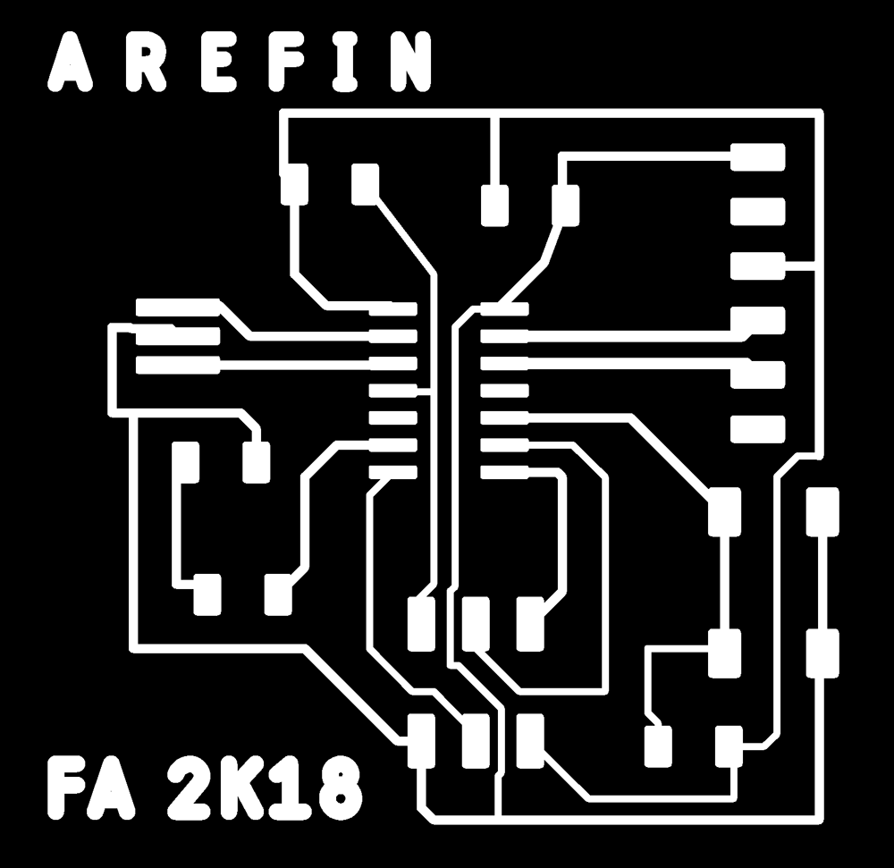
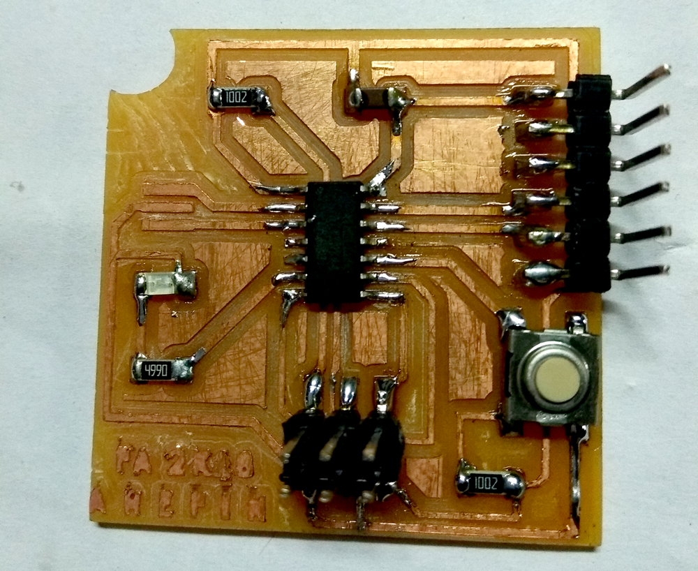
Board Design: After completing schematic all process now I shifting to the Board design panel by eagle software. I board design every step are described in below with images:
1. I moved the design component in middle of the windows
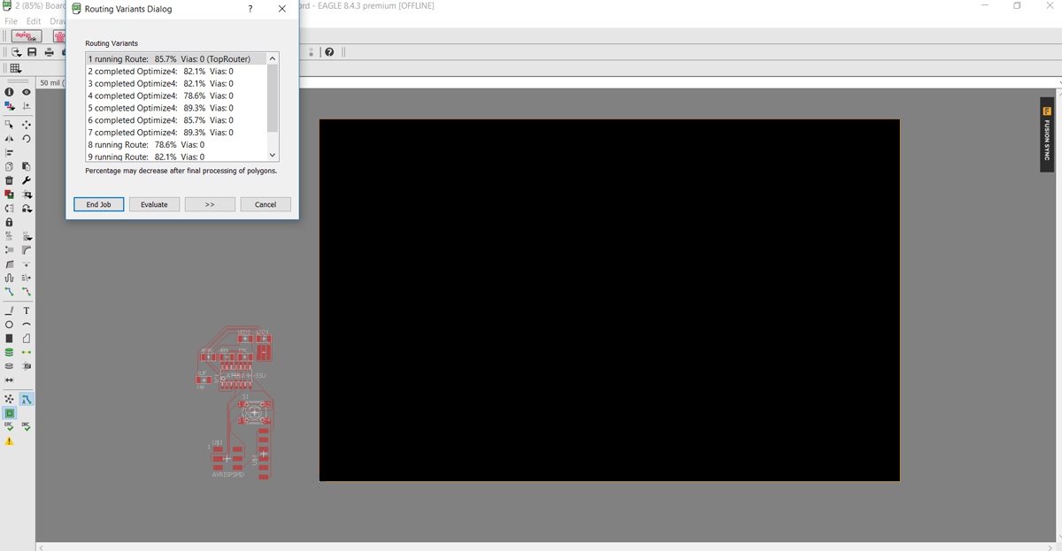
2. I used here auto routing
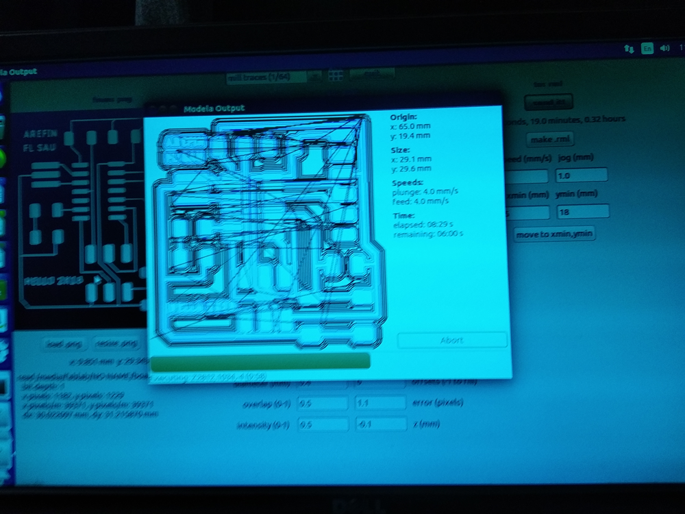
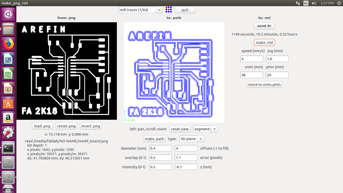
3. And then i export this images as a board traces to mill this design. But After completing my Milling there a problem i saw that is the all traces of wipe out from the board due to the proper dimension of the board and trace line width. (0.13 mil)
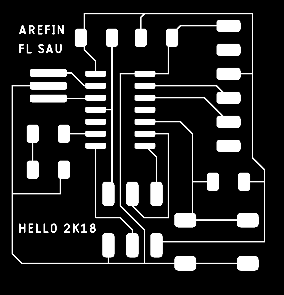
4. After that I redesign my board again and first i fixed dimension of the board and show the given hello board traces as a reference with arrange the button and the LED. I routing this board as manually with the width of (0.40 mil) traces line. I only use (0.15 mil) traces line in two line for the inner path of ISP and Attiny44 to connect MISO/ GND /RST line.
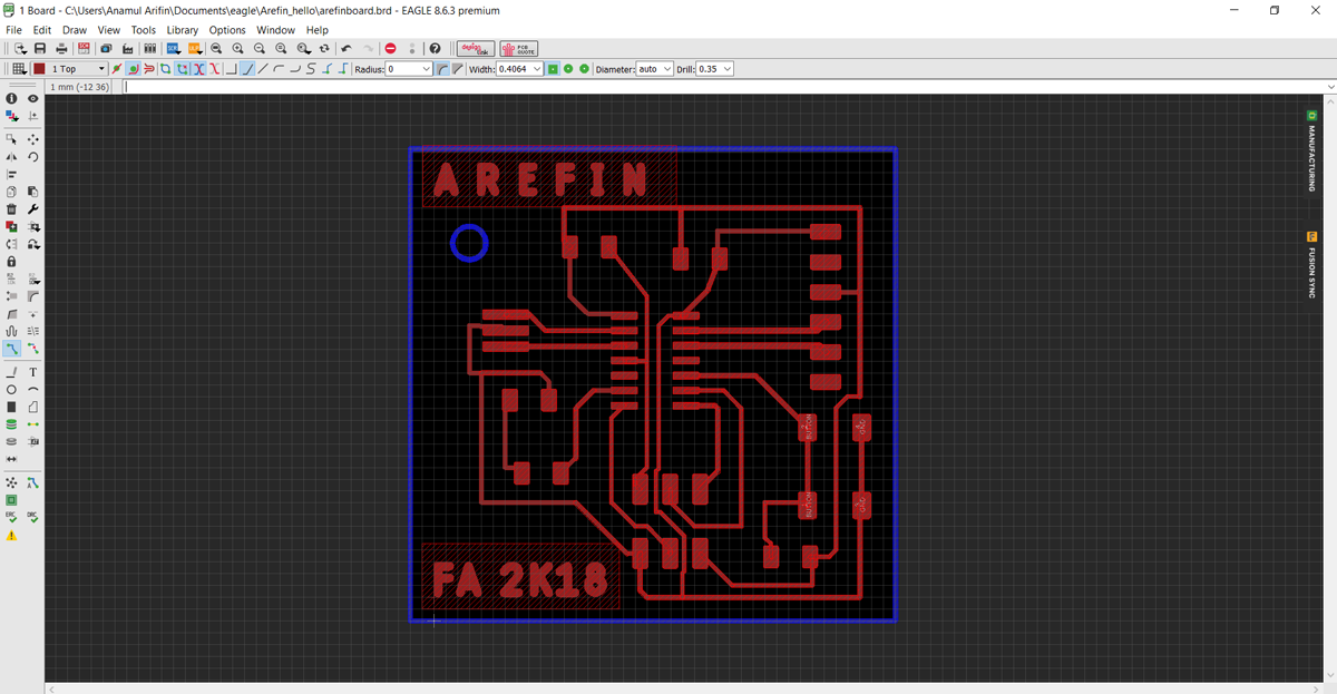
5. After Manually routing the board I checked the DRC for proper line, here it show several error like, I add my name in the board which is cross the outline of VCC and the another in some trace line of the micro-controller are also so close. But I approved manually. If i follow the DRC and reduce the traces width then during milling the all traces wipe from the board. I don't know is it software problem or the milling machine can't give the proper output.
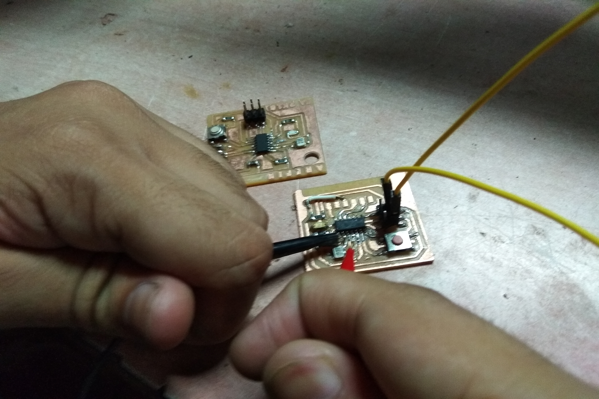
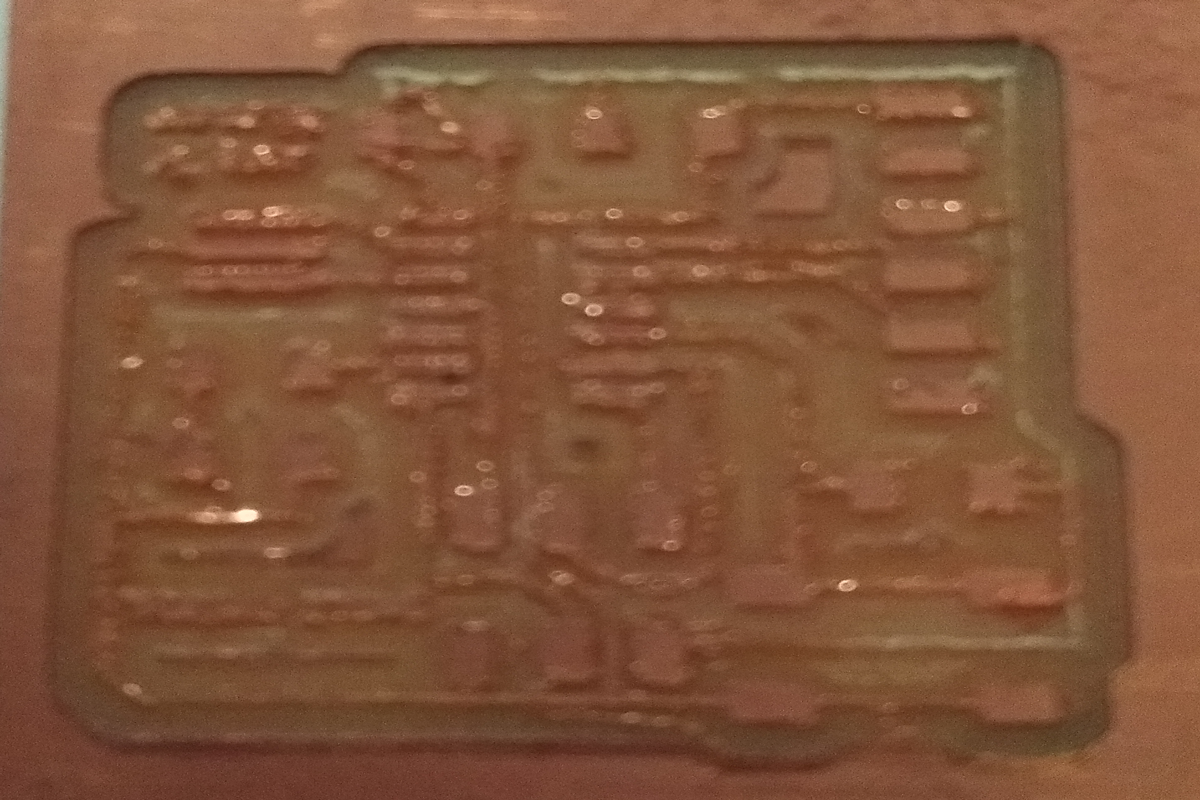
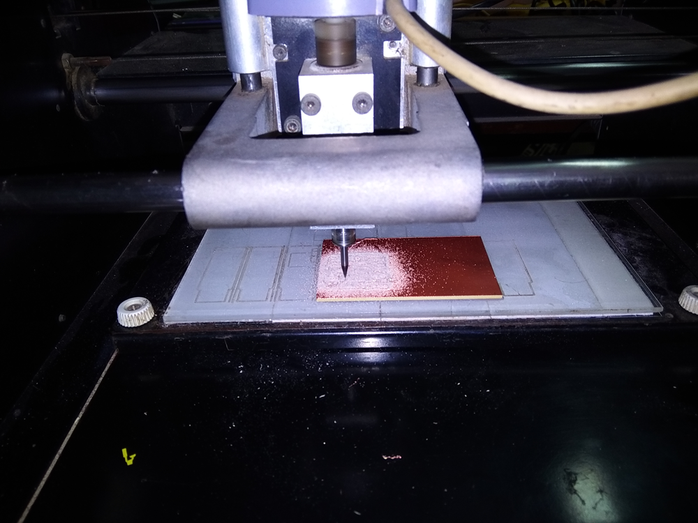
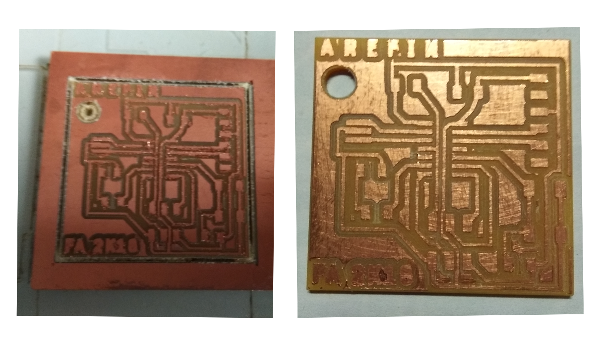
6. Milling: I follow the milling rules as we are doing for making the FABISP, I mill two hello board for my assignment. After milling the traces are not proper mill, after that i used filling bar for smooth traces in the board and also used knife for remove unwanted cutting traces.
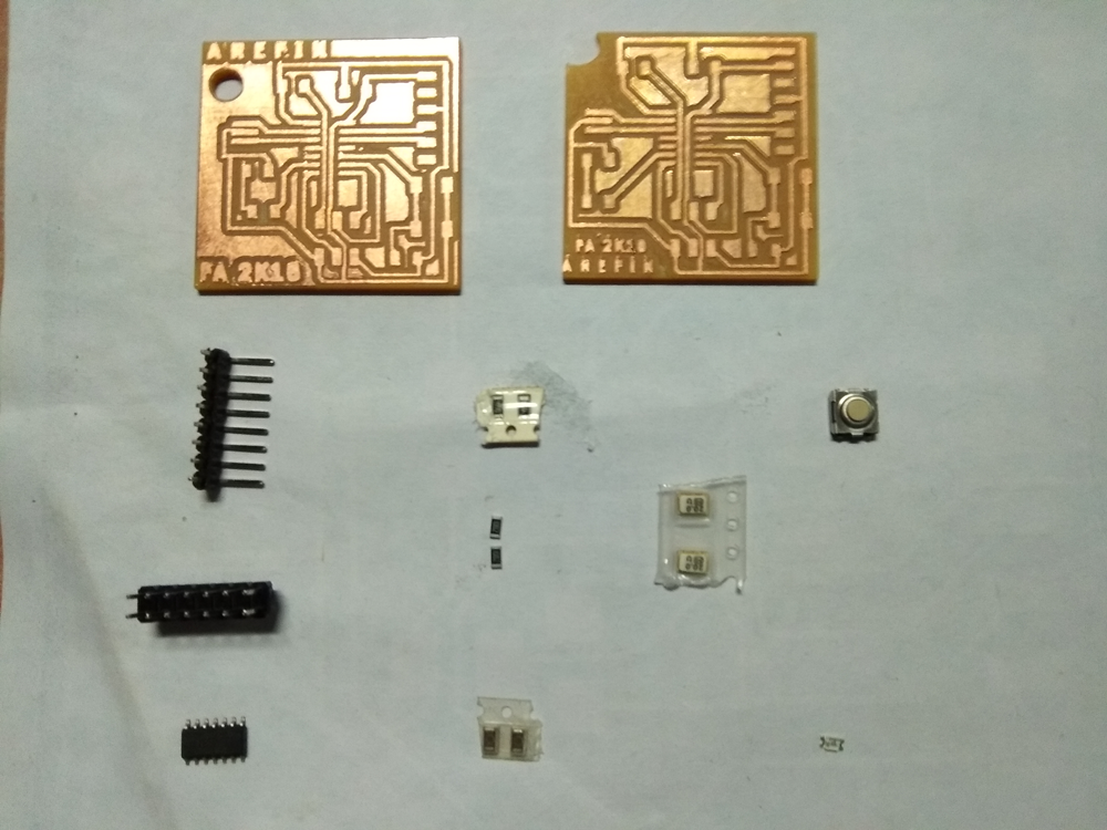
7. Soldering: I soldered the board as maintain the soldering rules
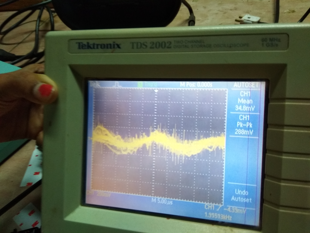
For this assignment we are testing our hello board by oscilloscope, and saw in the monitor that how the voltage are passes in the board and ow is looking the proper voltage curve. Generally the good soldering board are giving the rectangular curve but in my board i saw is zigzag curve which is denoted that the some where is problem to pass the voltage properly, then i remove the resonator from the board and re-soldered, then check again whats going on the board. Then it show as good as previous. After that i thought i re-milling my board again and soldering properly for proper programming.

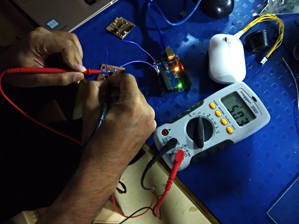
Power Testing: After soldering the test the board by attachment with on programmer and check just VCC and GND in all component where is how much voltage are in the board.