Networking and Communications
- 1. Design and build a wired &/or wireless network connecting at least two processors
- 2. Send a message between two projects
Networking and Communications
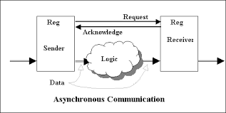
Decided to try and build an asynchronous serial communication network. According to Wikipedia - on Asynchronous Communication, it is the transmission of data without the use of an external clock signal, where data can be transmitted intermittently rather than in a steady stream. In asynchronous transmission, data is sent one byte at a time and each byte is preceded by start bit and stop bit. This site gives a comparison between synchronous and asynchronous transmission.
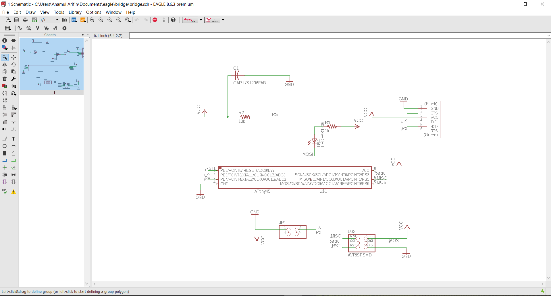
Asynchronous Bridge and Node Like I2C, it will have one bridge and 2 nodes to communicate with the computer via a FTDI interface. With reference to the class site, I would be referring to Neil's boards design, a hello.bus.45.bridge and hello.bus.45.node will be created in Eagle. I changed the placement of the different components in board and make the traces for vinyl cutting.
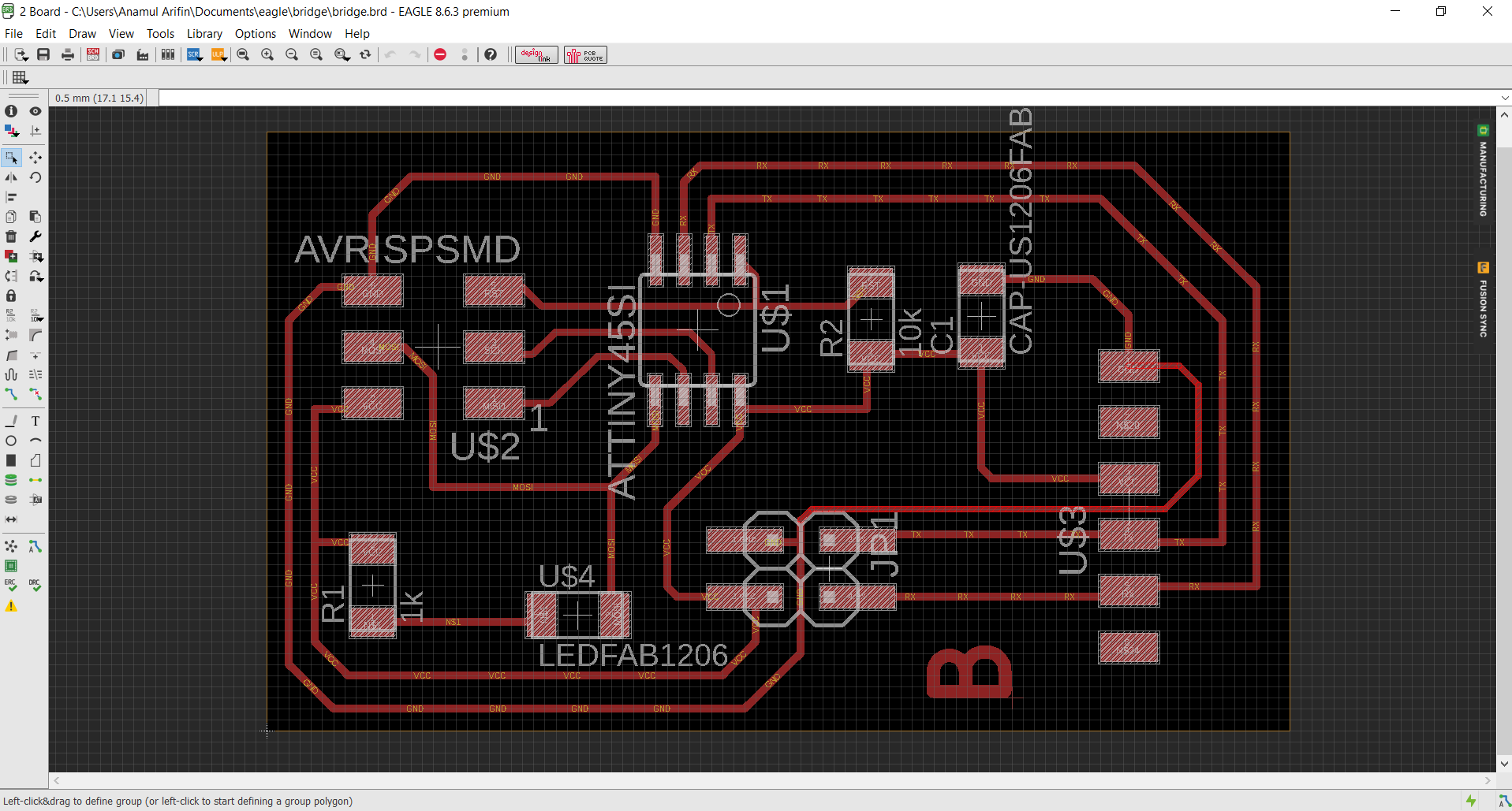
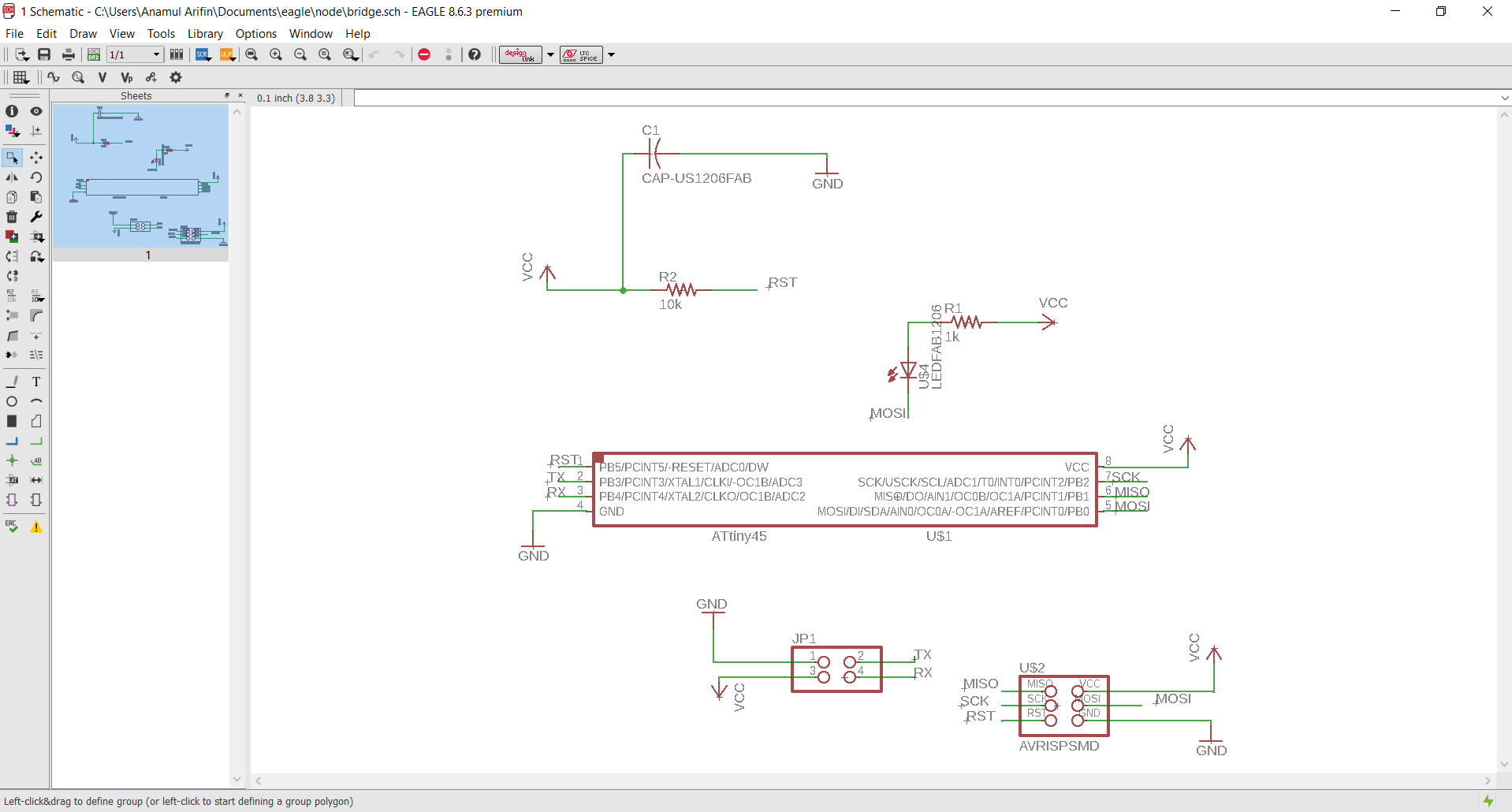
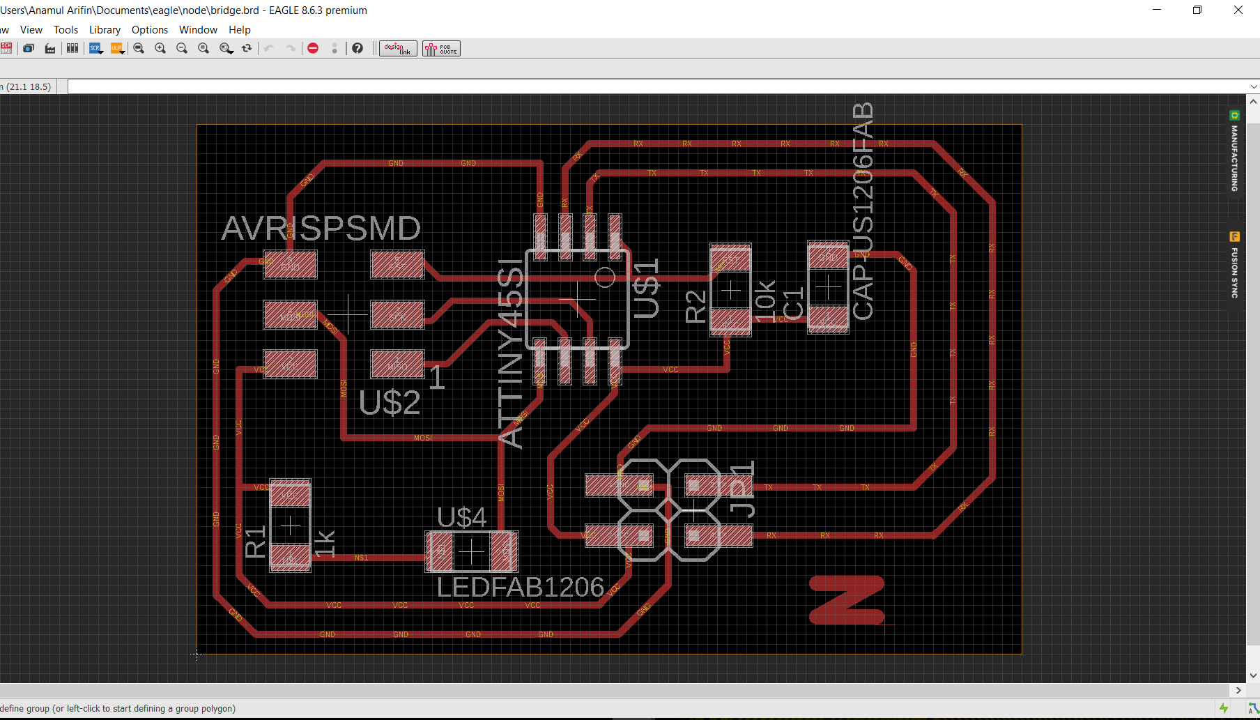
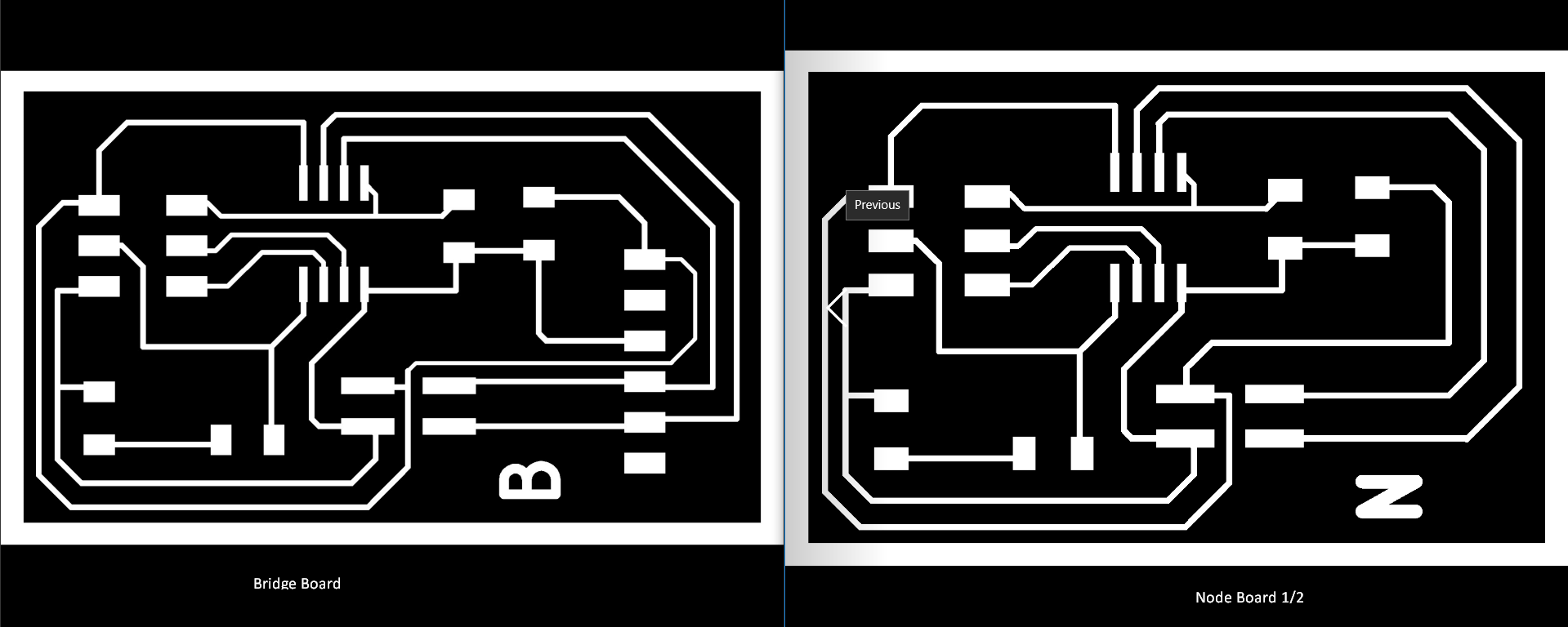
According to the PCB making i used PNG traces design in Roland Vinyl Cutter, Here I describe the process of the layer making of the copper flexible, first one transparent sheet and attached the copper film on the transparent sheet with double sided tape, If you want to keep it longer time without disturbing the track then use masking.
During soldering the flexible circuit then you need more concentration, don't apply longer time solder tip in the pad, use masking tape for holding it in the table, use few solder flask but remember it make high temperature on the circuit. Now for that you use mouth to blow the air after soldering each of the pads.
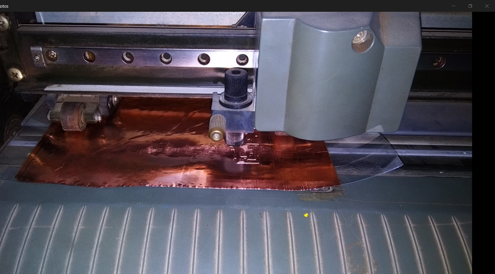
Cutting of the Copper sheet for circuit

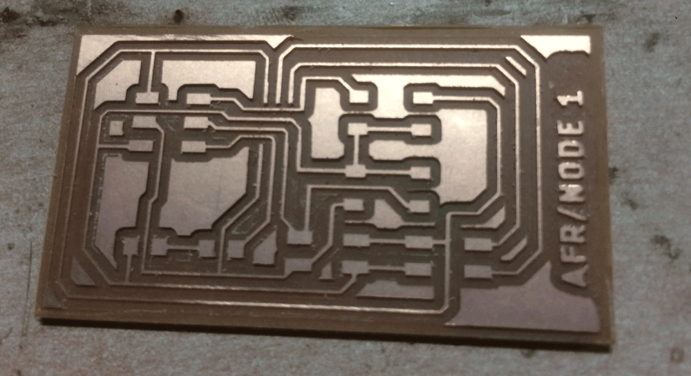
After cutting with Vinyl Cutter
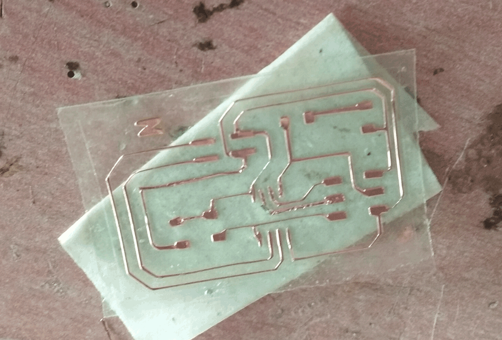
After removing of the other part of the board accept traces line.
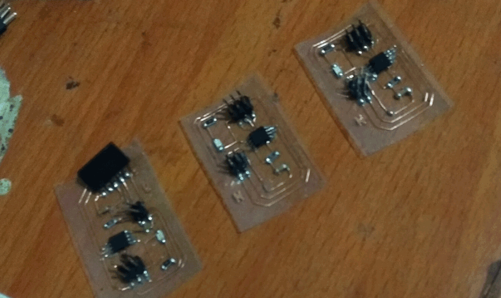
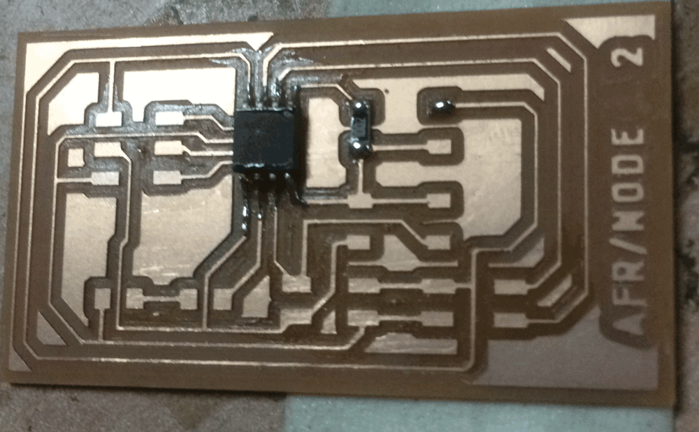
After soldering the process, it look like same as the other board.
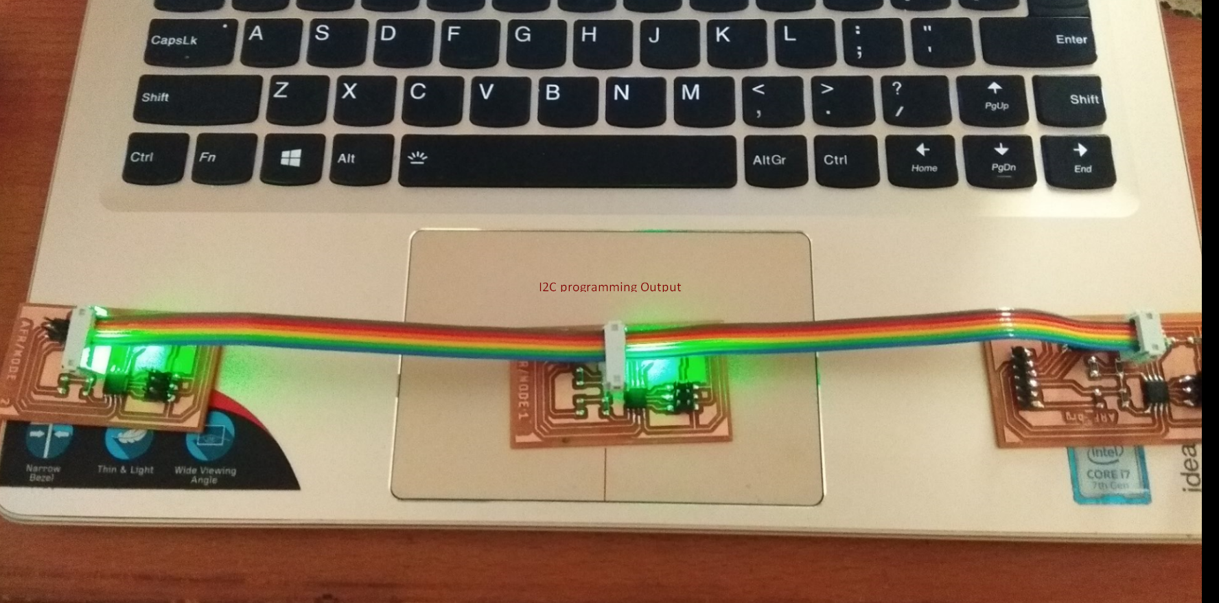
after soldering testing of the flexible board then i going to program it and its burn the program as well but when i connected with FTDI here is showed the three board are blink at a time.First I continue the programming part in the bridge and node board
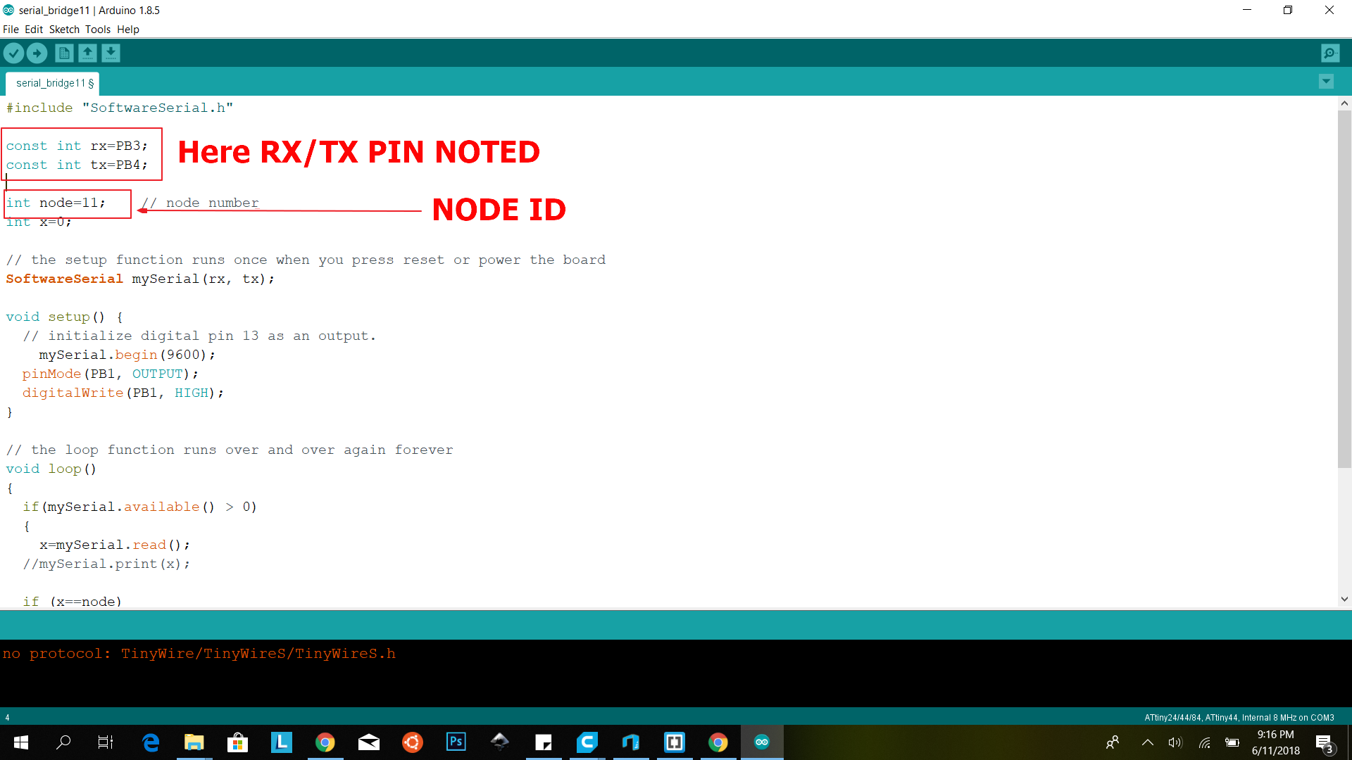
The code for Bridge serial communication with node
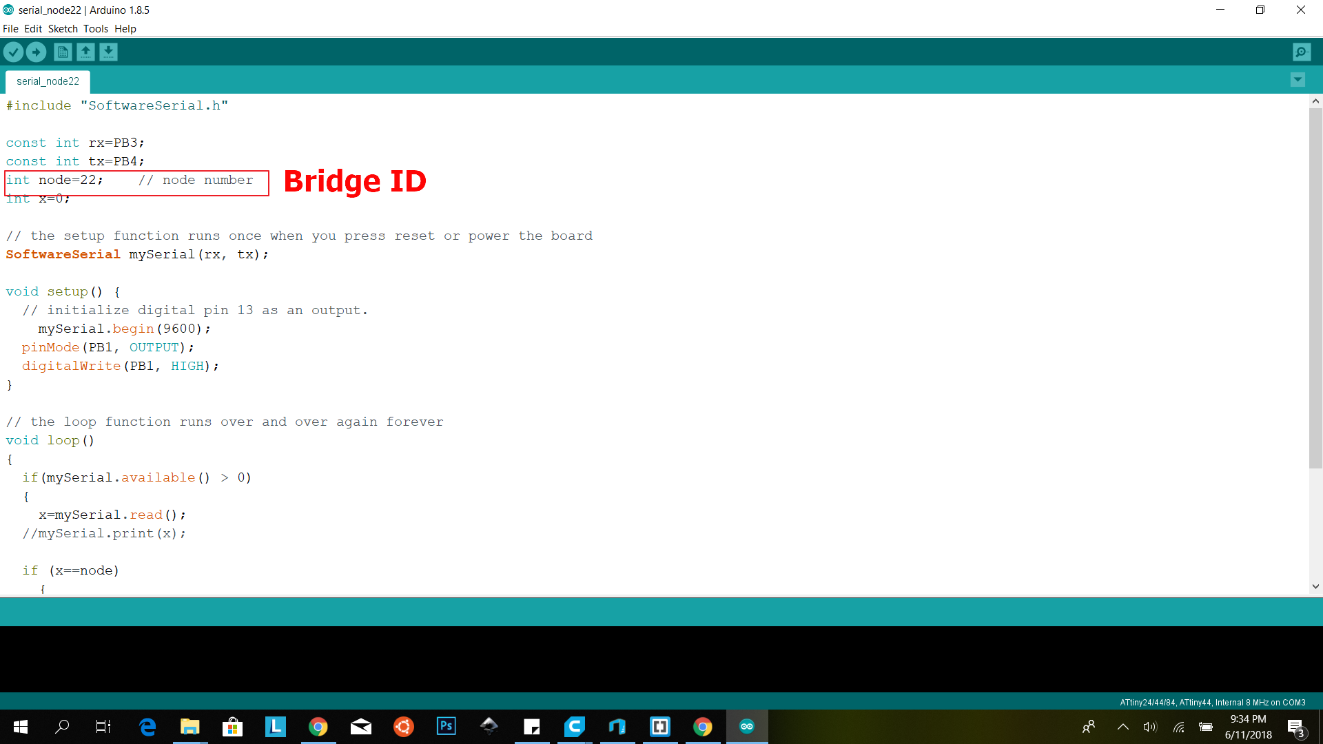
Node 1: Same code but need to change the node ID in the code
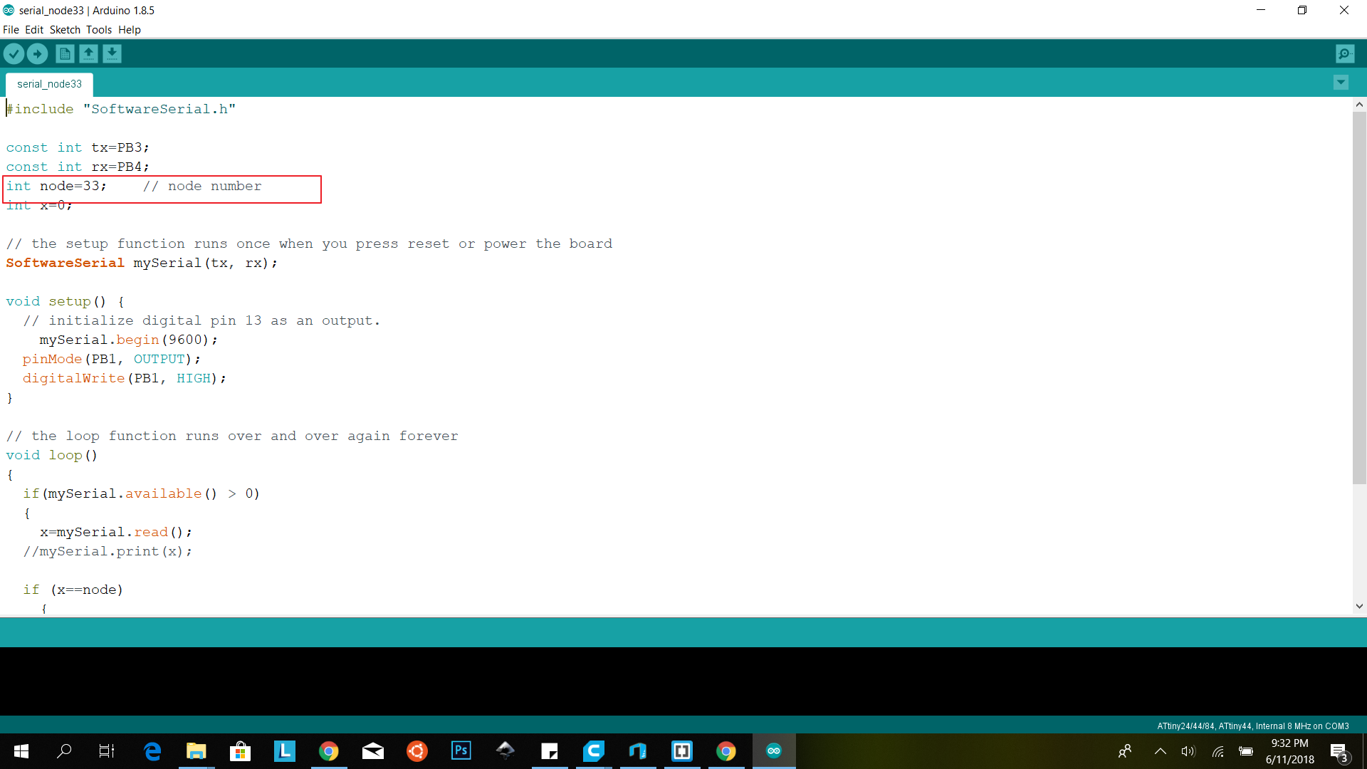
Node 2:Same code but need to change the node ID in the code
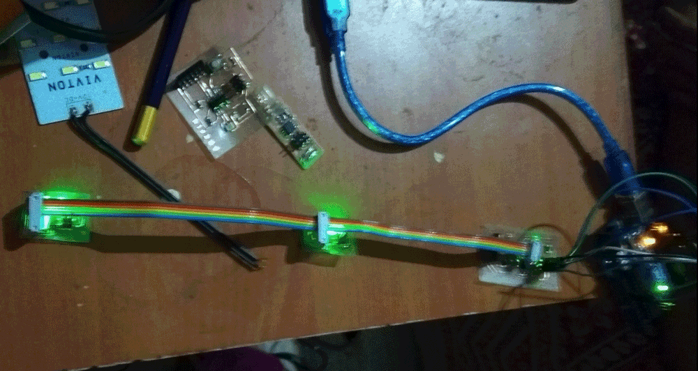
The image during programing
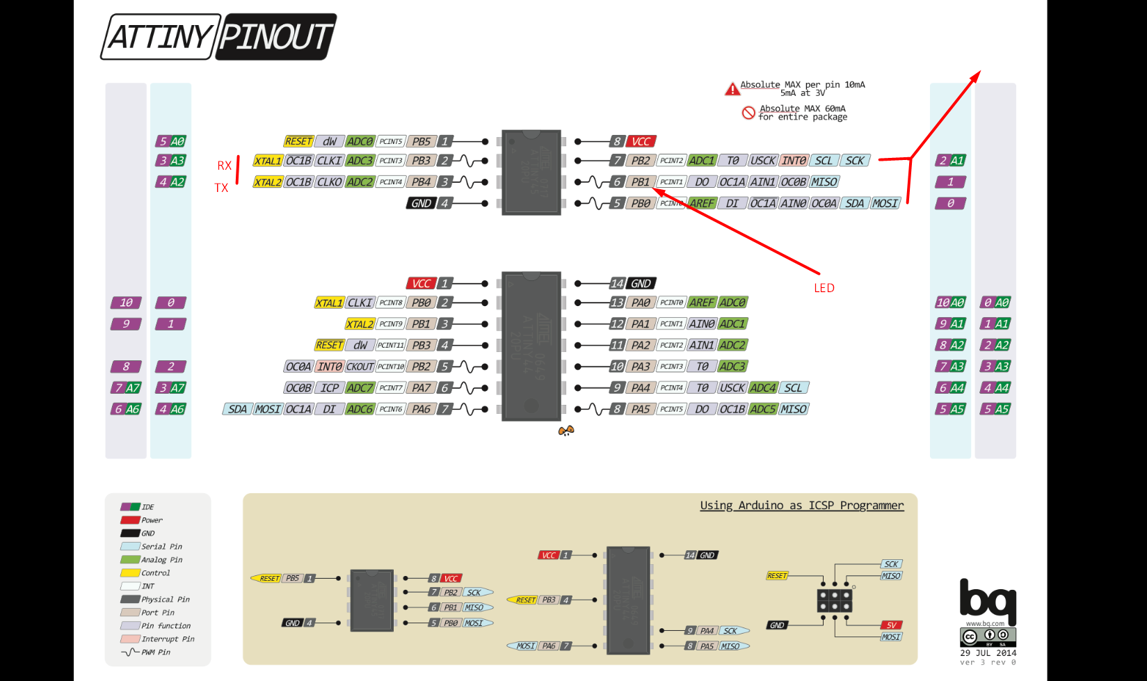
After doing everything, but i here i faced one problem that was the handling of the flexible circuit is quit hard and you should always remain concentrate with the attachment and detach of the PIN and FTDI. when i was doing this that time the traces are wiped out . I decide to again milling the board. Here in Asynchronous communication are sending and receiving data signal by RX/TX pin where as in noted PB3/PB4 pin. Bridge, Node 1 and Node 2 are sending data by same protocol, In serial monitor I visualize it by FTDI with RX/TX pin.
Next attempt is to make 3 boards (one bridge and 2 nodes) to communicate with one another. With reference to the class site, I would be referring to Neil's boards in my design, a hello.I2C.45.bridge and hello.I2C.45.node will be created in Eagle. Here I was decided to make I2C and Serial communication port in one board. I2C protocol are work on SCK and SDA on the other hand the serial are working with TX/RX.
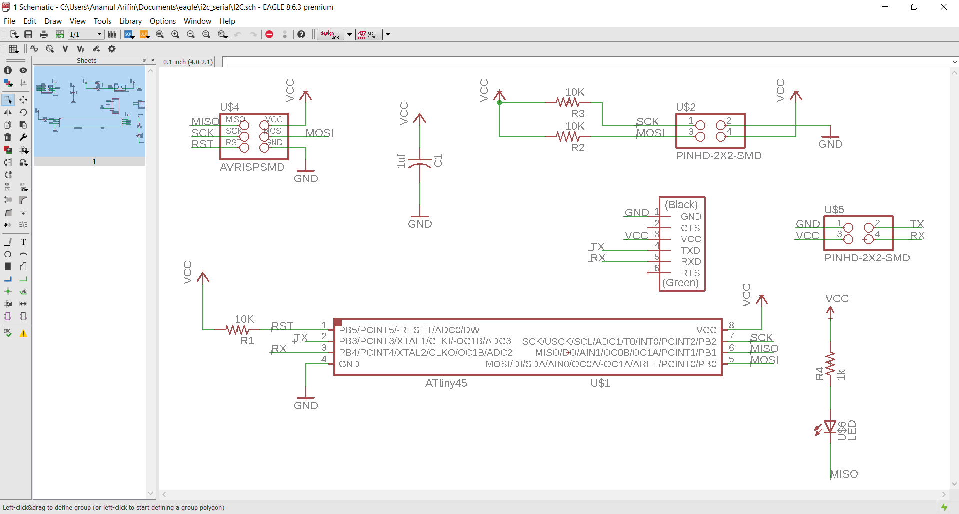
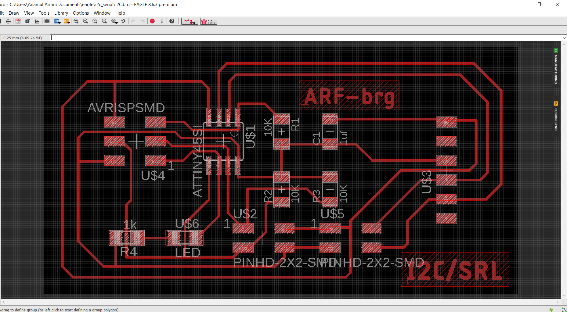
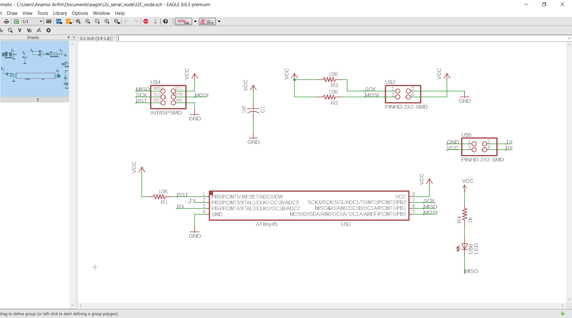
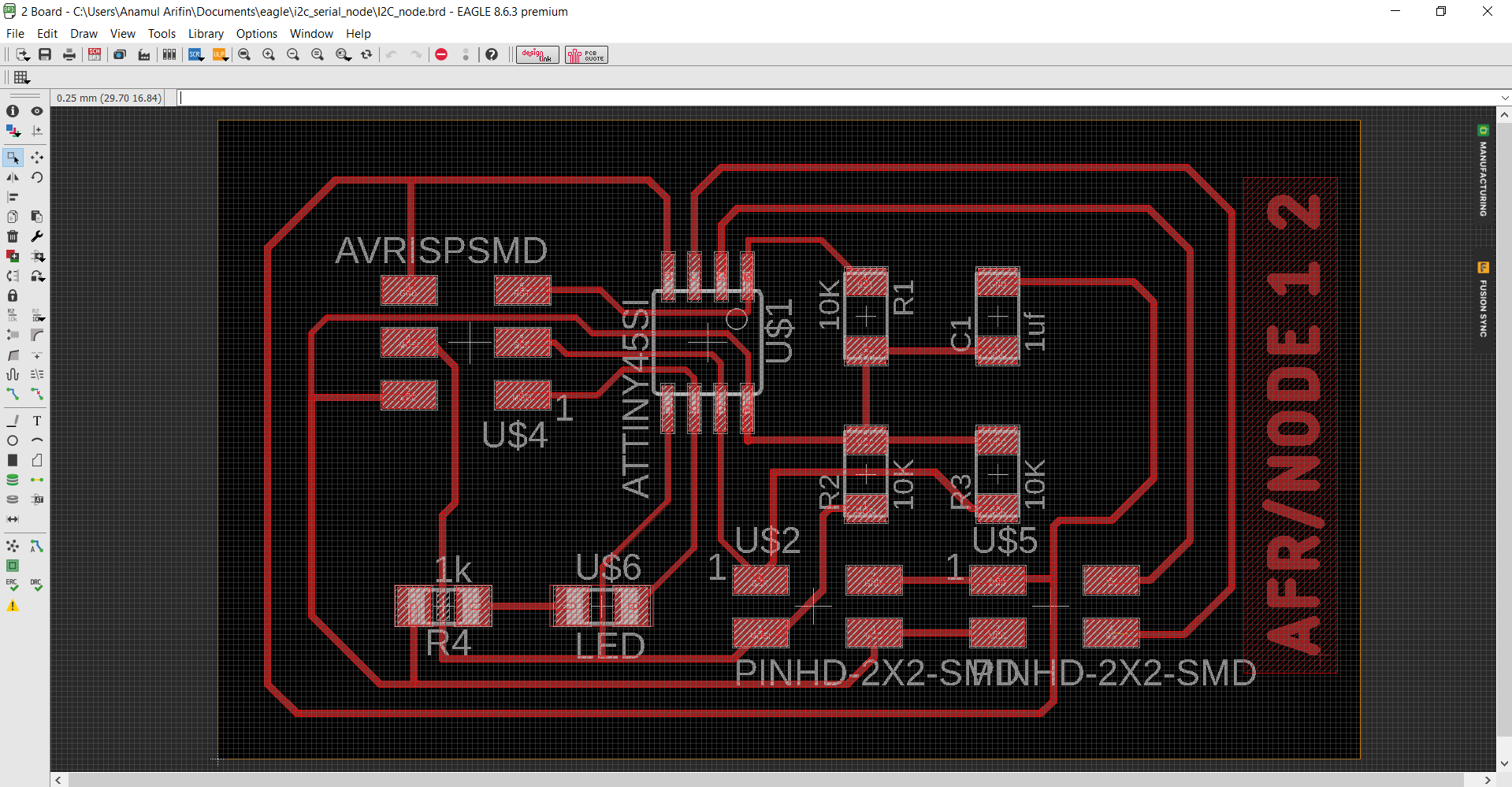
Board design for I2C communications
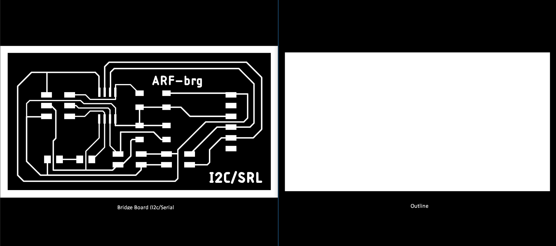
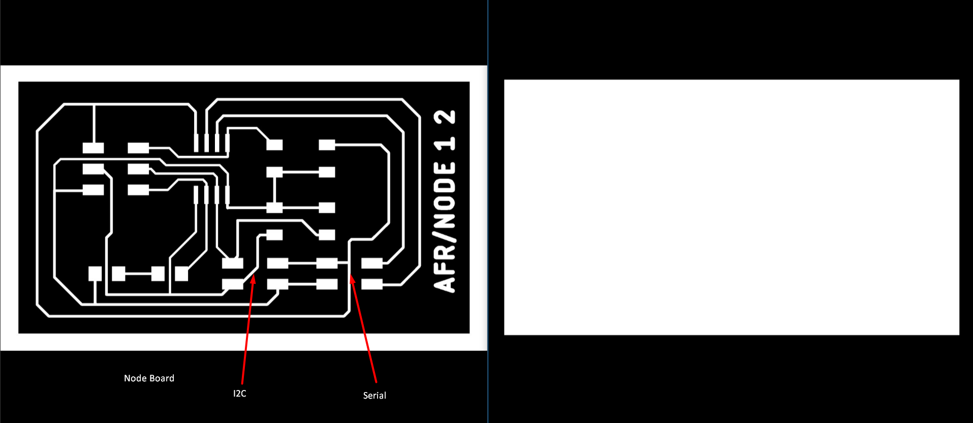
Here for milling and soldering for circuit i follow the same process which i was did for previous assignment, for traces milling i used 1/64 end mill and for cutting i used 1/32 end mill.
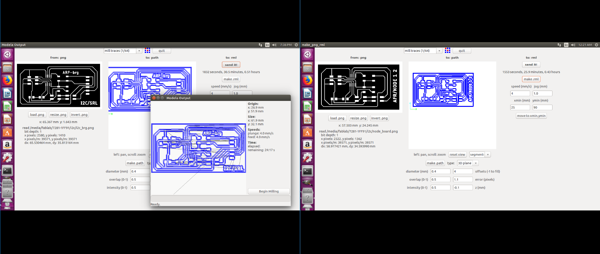
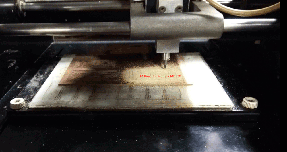
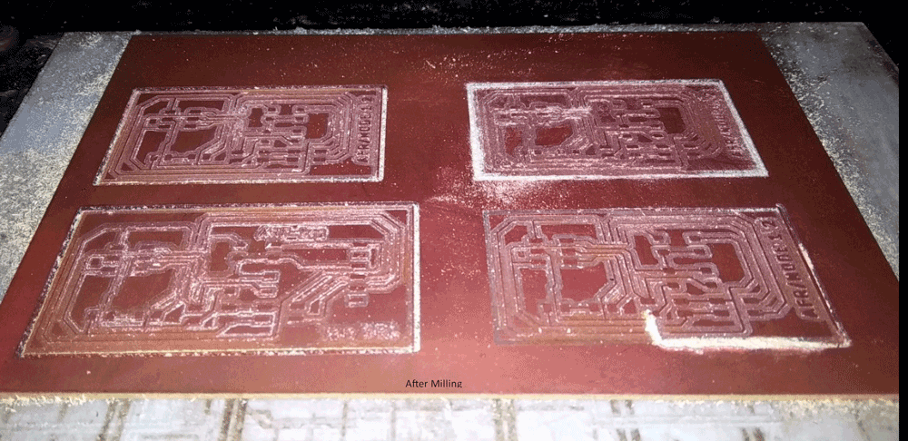

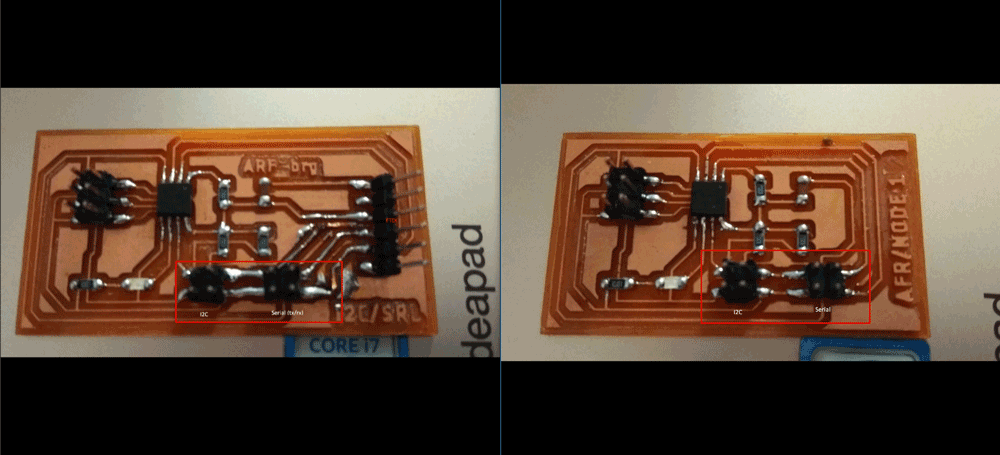
This is the final circuit for asynchronous and synchronous communication between three micro-controller
The I2C bus is a half-duplex, synchronous, multi-master bus requiring only two signal wires: data (SDA) and clock (SCL). These lines are pulled high via pull-up resistors and controlled by the hardware via open-drain drivers, giving a wired-AND interface. I2C uses an addressable communications protocol that allows the master to communicate with individual slaves using a 7-bit or 10-bit address. During communication with slave devices, the master generates all clock signals for both communication to and from the slave. Each communication begins with the master generating a start condition, an 8-bit data word, an acknowledge bit, followed by a stop condition or a repeated start. Each data bit transition takes place while SCL is low, except for the start and stop conditions. The start condition is a high-to-low transition of the SDA line while the SCL line is high. A stop condition is a low-to-high transition of the SDA line while the SCL line is high. The acknowledge bit is generated by the receiver of the message by pulling the SDA line low while the master releases the line and allows it to float high. If the master reads the acknowledge bit as high, it should consider the last communication word not received and take appropriate action, including possibly resending the data.
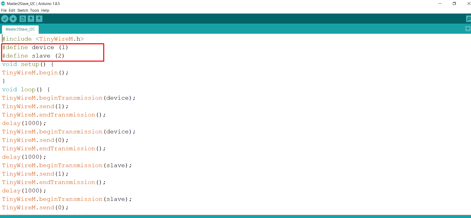
Here inside of the code I define two different slave ID for detected by the micro-controller with specific ID they are communicate each other by a definite time delay. This is the code for master board controller
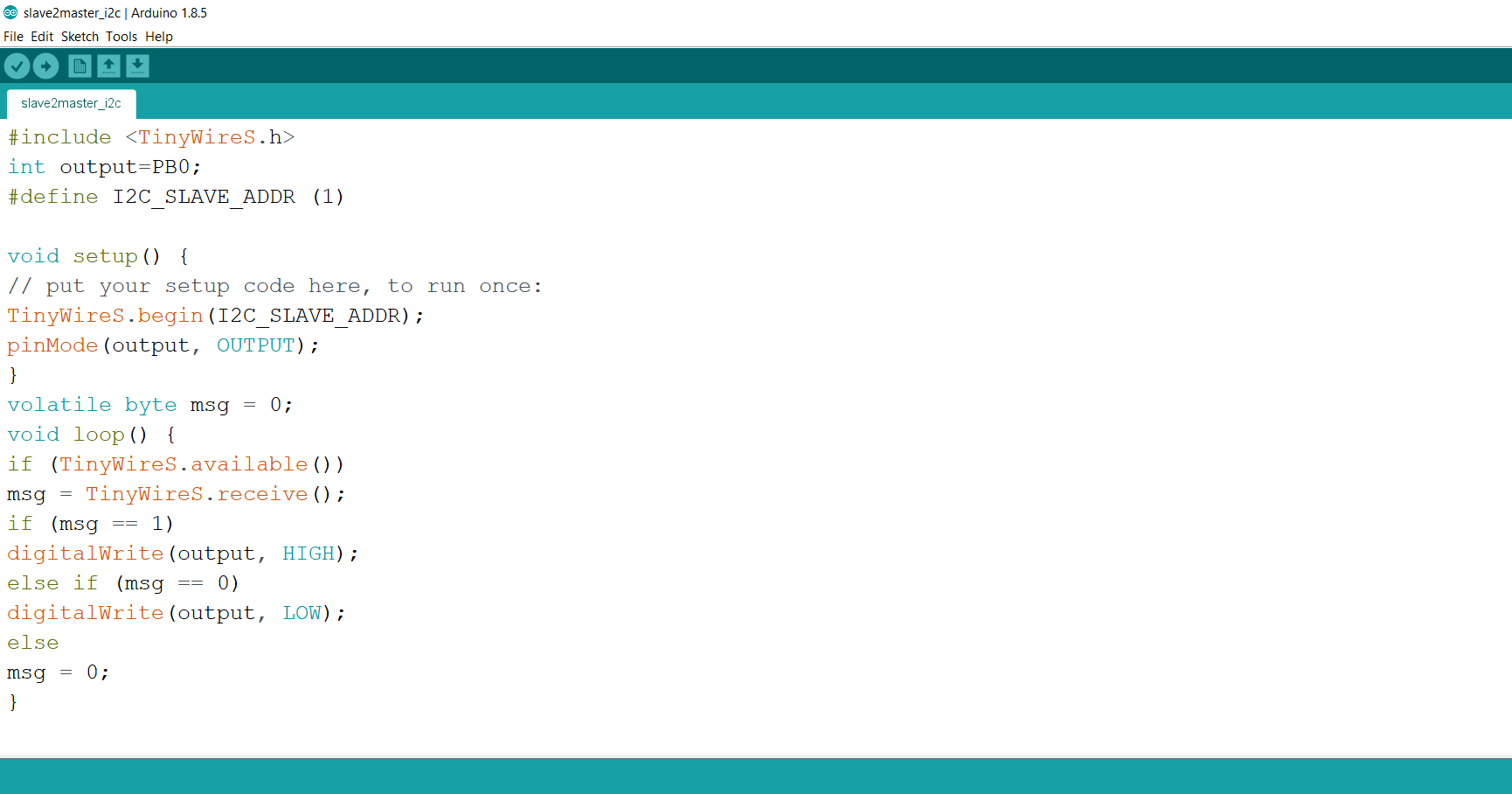
Slave I: This is the code for slave I ID for define it
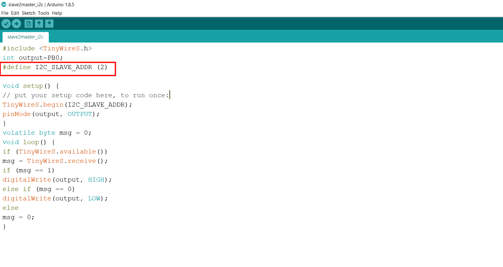
Slave II: This is the code for slave I ID for define it
Now I saw a one thing that is when i connected each of board as three ribbon jack then are show the blinking the LED with definite delay of time. Each of the LED are blow with creating a theme. Check in the video in below:
Again I want to test asynchronous communication between three board. I used my same board which is used for I2C communication, I design the board for two purpose. Here I test it in doing programming by neil's C code by Arduino and let see what happen.
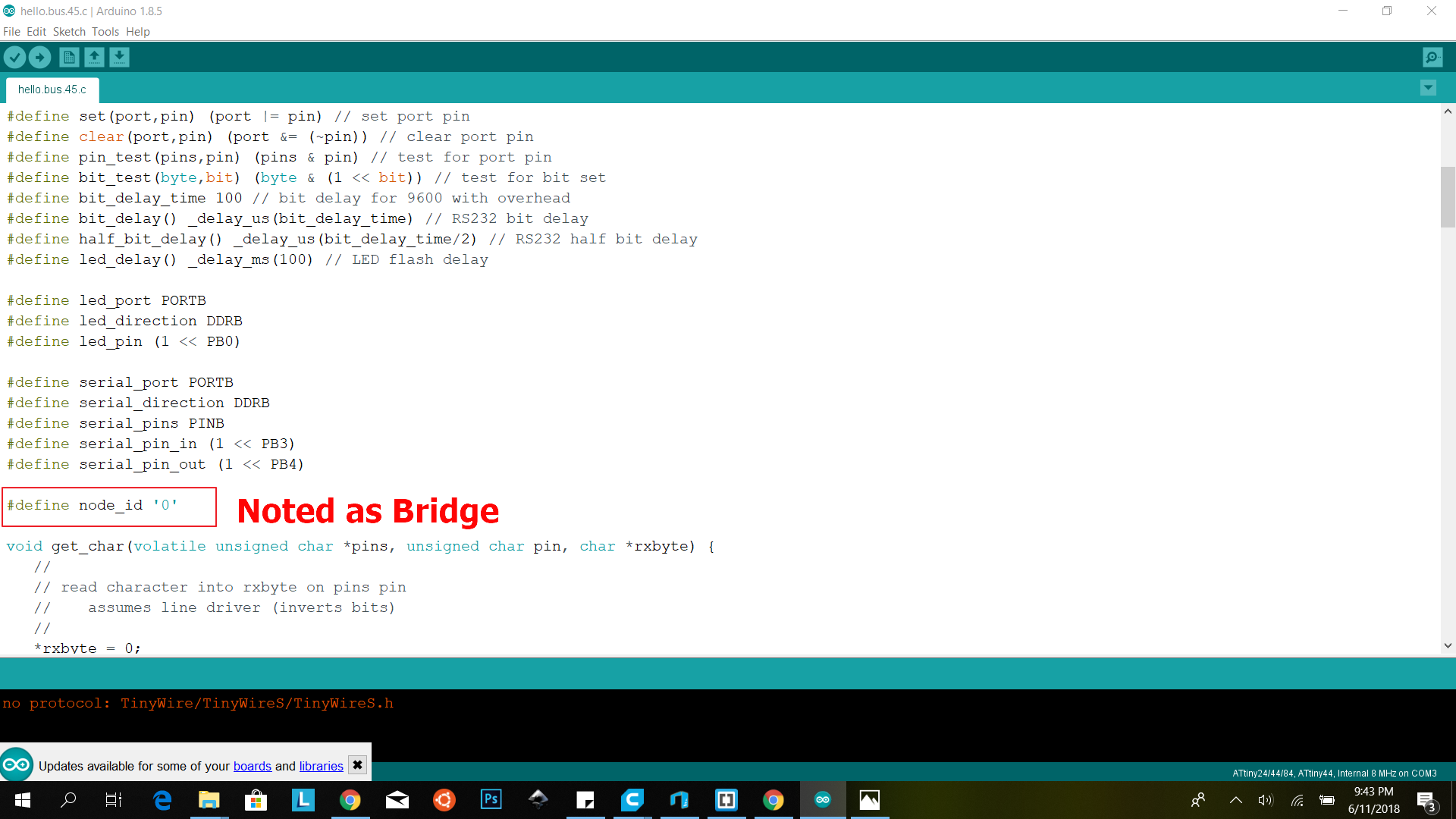
Code for Bridge and here I define this bridge as one definite number.
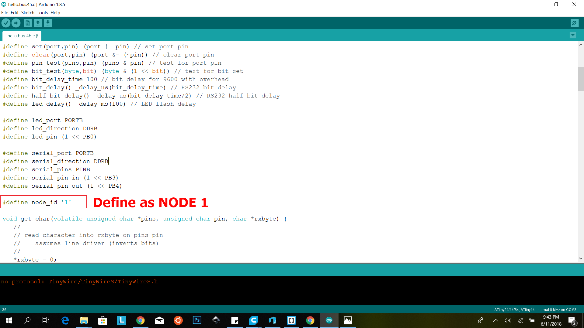
Node 1: Here i define this node ID for calling by serial monitor of Arduino
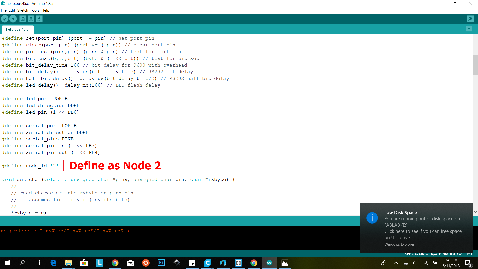
Node 2: Here i define this node ID for calling by serial monitor of Arduino
After programming I connect each of the board as serial one by one with ribbon cable with VCC/GND and TX/RX pin of each of board.Then I attached a FTDI cable with bridge board, in Arduino IDE here in tools menu change the serial port and open the serial monitor. Now I called each of the node and bridge as their defined ID where I defined them in CODE. IT'S BLINK But is it not the specific board. it blink all together. I tried to find out several times its happening same result. I check by Arduino and with RX/TX pin for data sending, but its happening same result. Lets see in the video in below: