
Week Four
Assignment
What I did
Introduction
This week we were introduced to the topic 'Electronic Production'. This was a completely new topic for me as I didn't have any prior electronics knowledge. I had so many things to study in this week. Neil introduced us to different PCB fabrication techniques like etching, lithography etc. The method we use in our fab lab was a PCB milling technique.
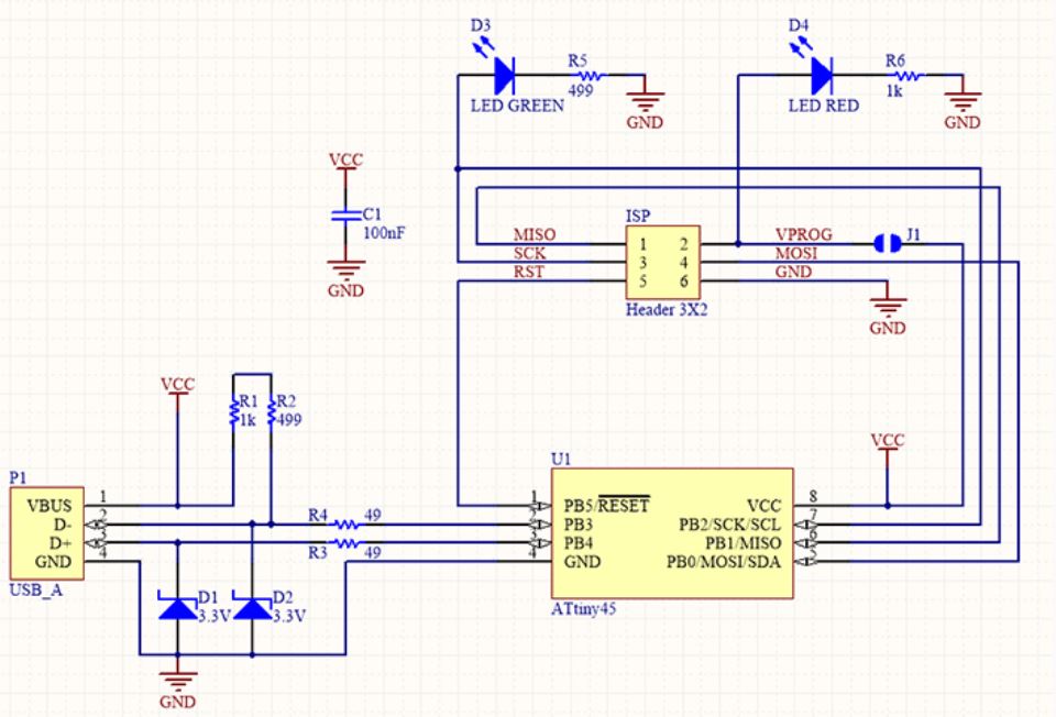
This weeks assignment was to make a Fab ISP (In-Circuit Serial Programmer) using PCB milling technique. An IsP is something that we use throughout the Fab Academy programme and its used to program the electronic boards. This weeks assignment includes PCB milling and Soldering of the components only. We are not concentrating much on the electronic designing and programming this week.
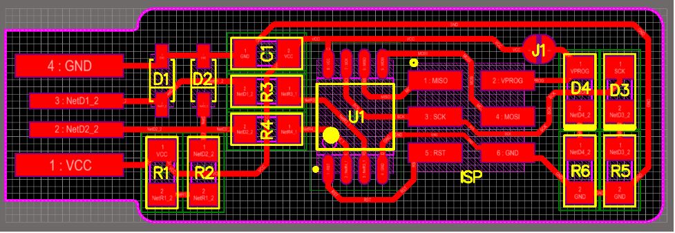
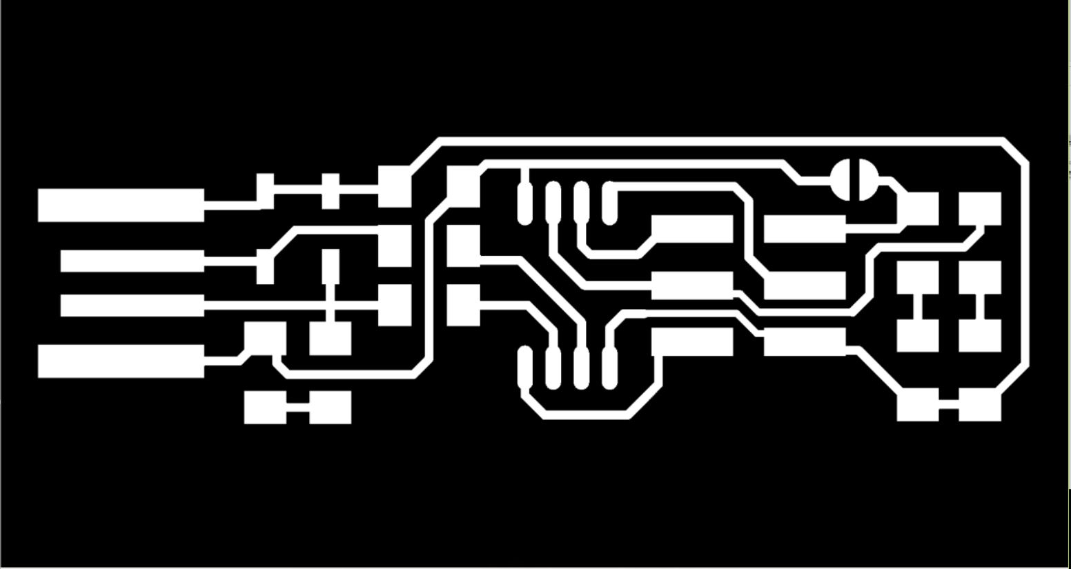
There are two Fab ISP 's available one ATtiny 45 and other ATtiny 44. I am planning to go with the first one since it has a much simpler design and have fewer components
ATtiny 45
I went through these files to start with my work. But before going into the project straight away I needed to get familiarised with the CNC milling machine that we used in our fab lab.
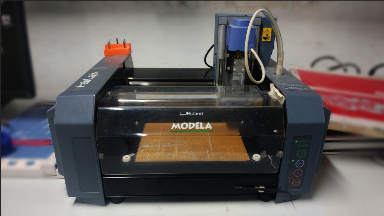
Modella MDX 20
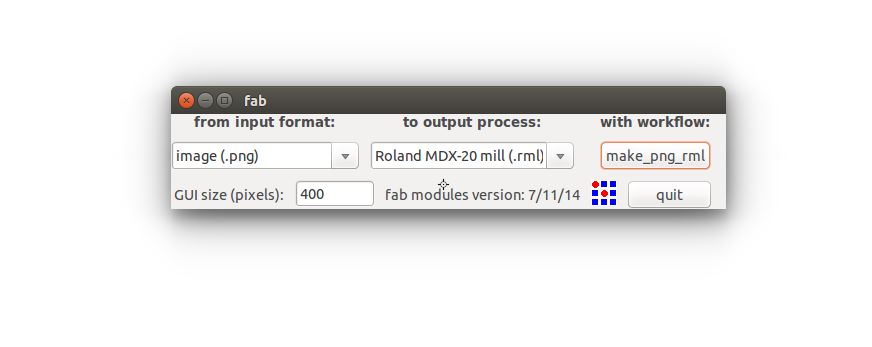
In our lab, we are using a Modella MDX 20 milling machine. Our instructor showed us how to use and set up the machine. We can set up the machine using a fab module similar to the way we used the Roland vinyl cutter.
The main things that we have to keep in mind before milling is the safe changing of bits. We are mainly using two kinds of bits a 1/64 inch and 1/32 inch. The first one is used for tracing purposes and the second one is used for cutting purposes.These numbers indicate the diameters of the bits.
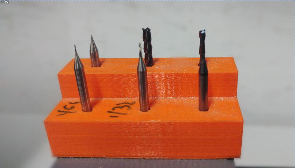
We have to be really careful while changing the bits because the tips of the bits are really small and likely to break on a very small impact. So, we always have to keep your fingers between the bits while changing them.
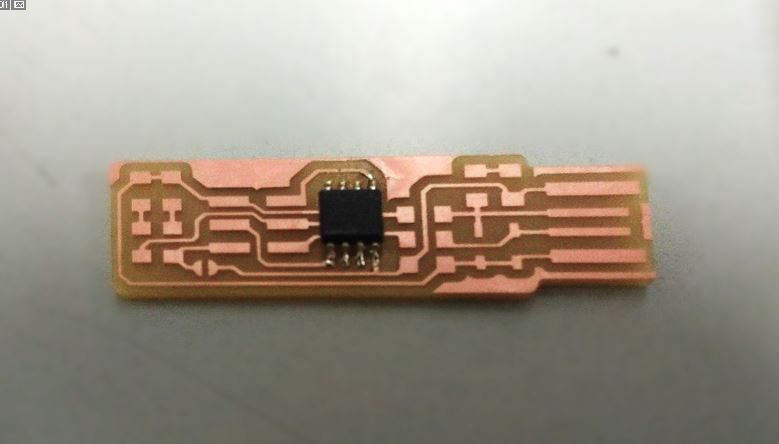
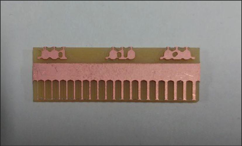
Milling PCB
The next step was to mill the PCB. The PCB board that we use in our lab is the FR-1 grade PCB. Our instructor has already given us some idea about fixing the board to the machine bed. We used a double-sided tape for fixing the same. After the board was fixed the next thing we had to do was to set up the fab module.
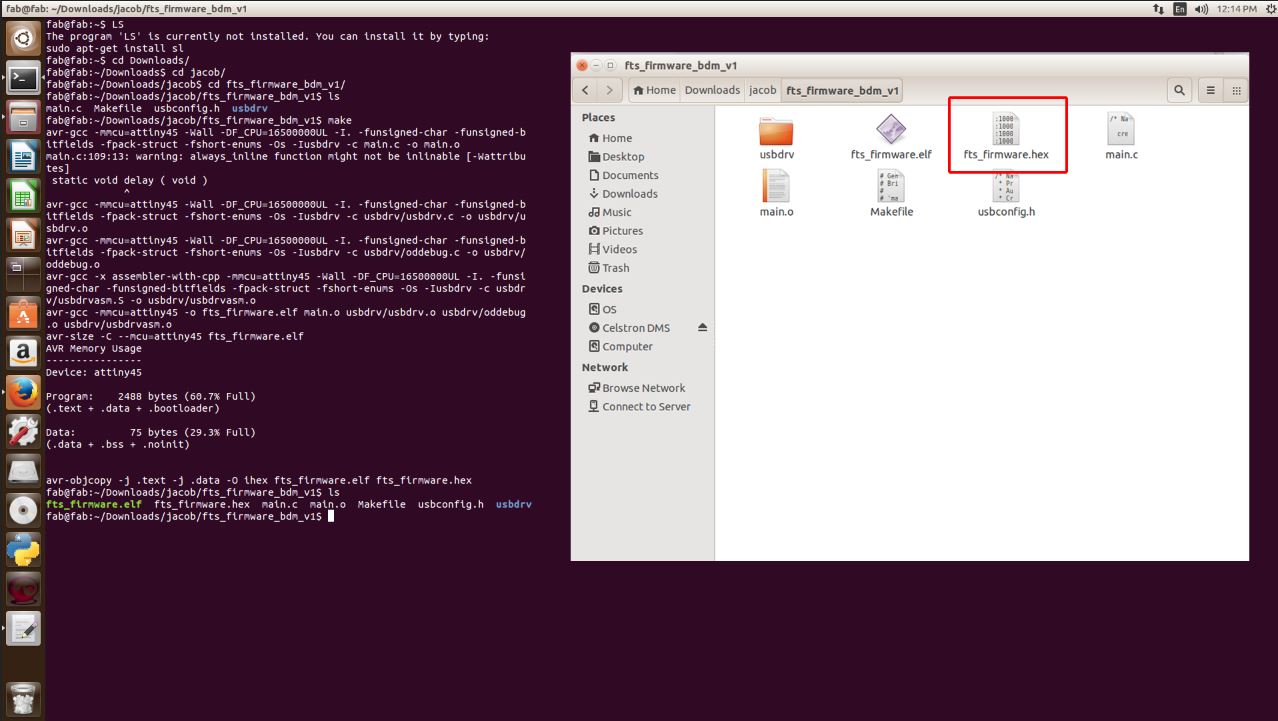
I took the PCB design files, images for tracing and cutting from here

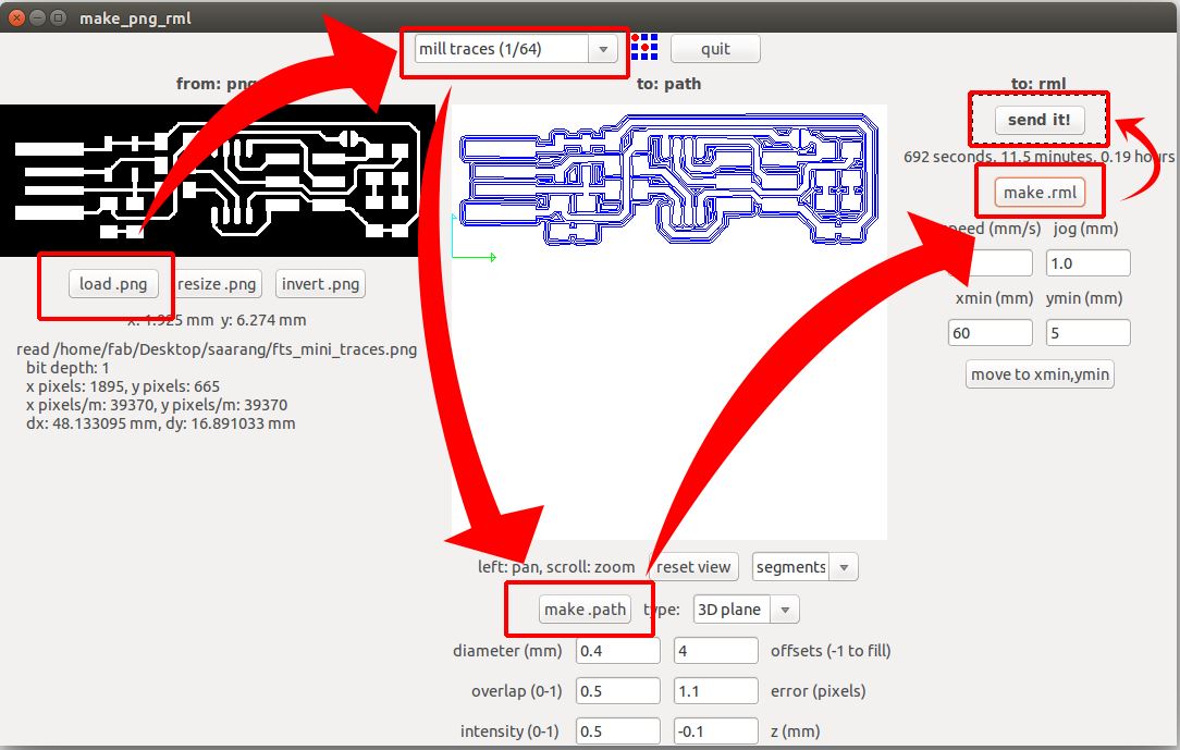
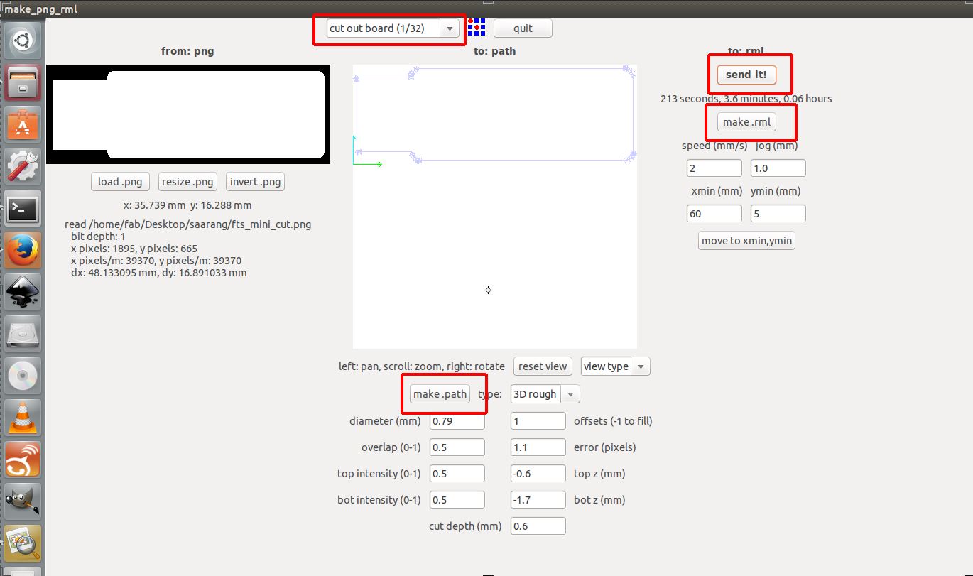
First, click on the 'view' button in the Modella to move the bed to the front portion so that you can place the PCB on to the bed. You can also change the bit now. Select a 1/64 bit as you are doing the milling process first.Open the fab module using the command 'fab' then select 'png' in the 'input format' section and 'Roland MDX-20 mill' in the 'output process'.
Load the png file to the software and click on the option 'make path'. Also, change the default option to 'mill traces (1/64)'.Now select appropriate X and Y value by changing the Xmin and Ymin value.You can set the Z value by using the 'up' and 'down' arrows in the Modella machine. This can get a bit tricky at times so just use the tightening screw to adjust the bit position so that it just touches the PCB.
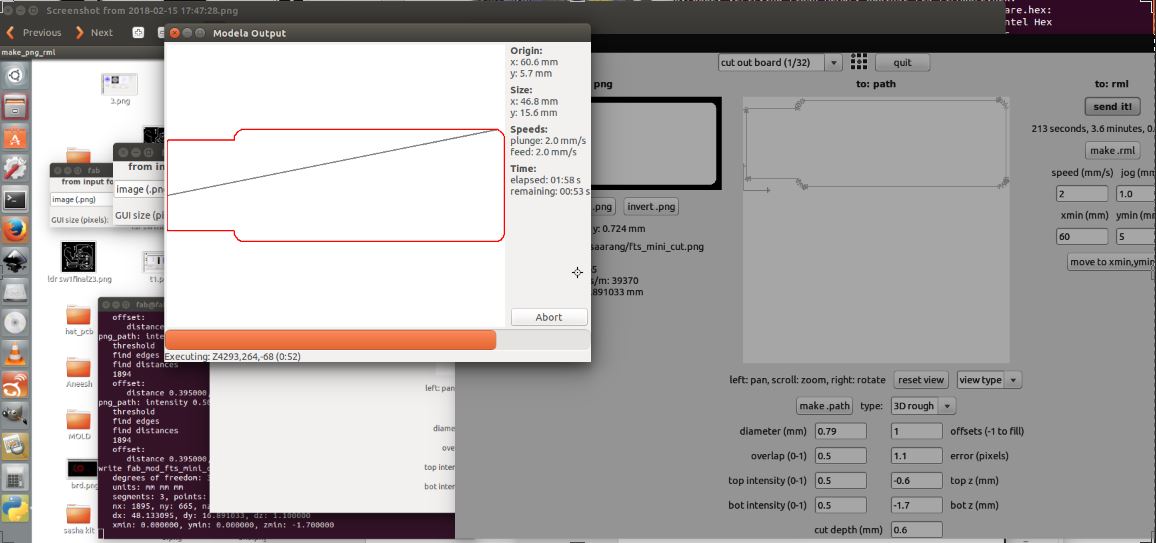
I changed the velocity to 2 mm/s for the safety purposes. Always remember your Xmin and Ymin value as they are required for setting positions at the time of cutting. Now select click on the 'make .rml' button and then 'send it' button. Click on the 'Begin milling' option in the window that appears.You can see the live status of your milling process in the window.
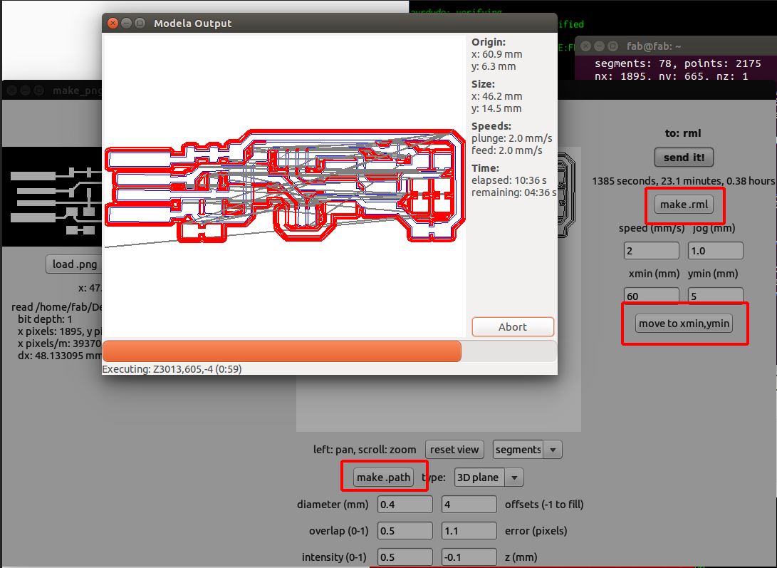
The next step is the cutting process. In order to start the cutting process first, I have to change the drill bit to 1/32 and adjust the Z value. Load the 'cut out image' and follow the same procedures as in the milling process to start cutting.
I adjusted the Z value using the 'down' button in the Modella machine. I couldn't accurately control the Z value using buttons and it went a little deep than required. But I thought it would be okay and started Milling. The drill bit broke instantly and I had to replace the bit. The next time I carefully adjusted the z value by loosening the drill screw using an Ellen key.
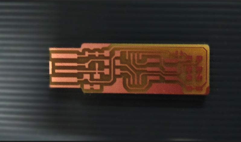
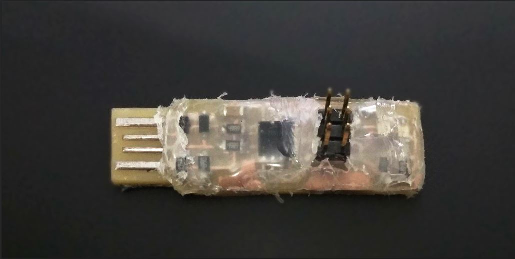
There were some small bits of copper on the PCB which I removed using a penknife. This was the final piece that I received.
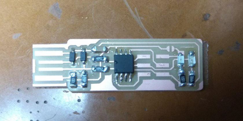
Soldering
The next step was to start soldering the components. I had a minimum experience in soldering from my college days. But I've never soldered an SMD (Surface Mount Devices) before. So it was kind of a challenging task for me. These were the components I took for making the ISP.
I took me some time to sort out each component from their respective boxes and my friend Salman also helped me with it.Now it was time to start the soldering
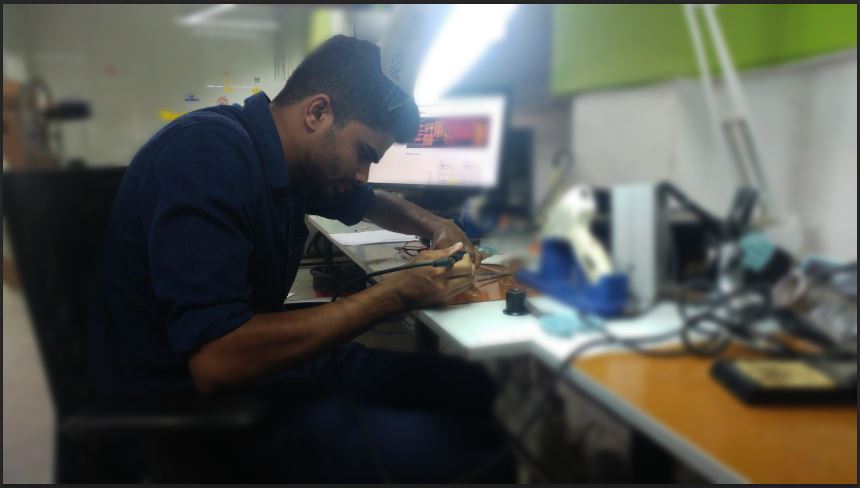
I started with the IC first. My friends at fab lab gave me some tips on how to place your board, how to feed the lead, etc. I really enjoyed this process because this was something new to me. Initially, I used the magnifying lens for soldering but then I found it really difficult to judge the distances and the movement of soldering iron looking through it. I even got a small burn on my fingers. So after a few attempts, I started soldering without using them. With my shaky hands, it took me around 20 min to finally fix my IC :D.
Fixing rest of the components was easy apart from figuring out the polarity in LED and Zener diode.I checked the continuity in each components in order to confirm the current flow between them usning a multimeter. I also studied how to remove the excess solder using a wix.
Programming the ISP
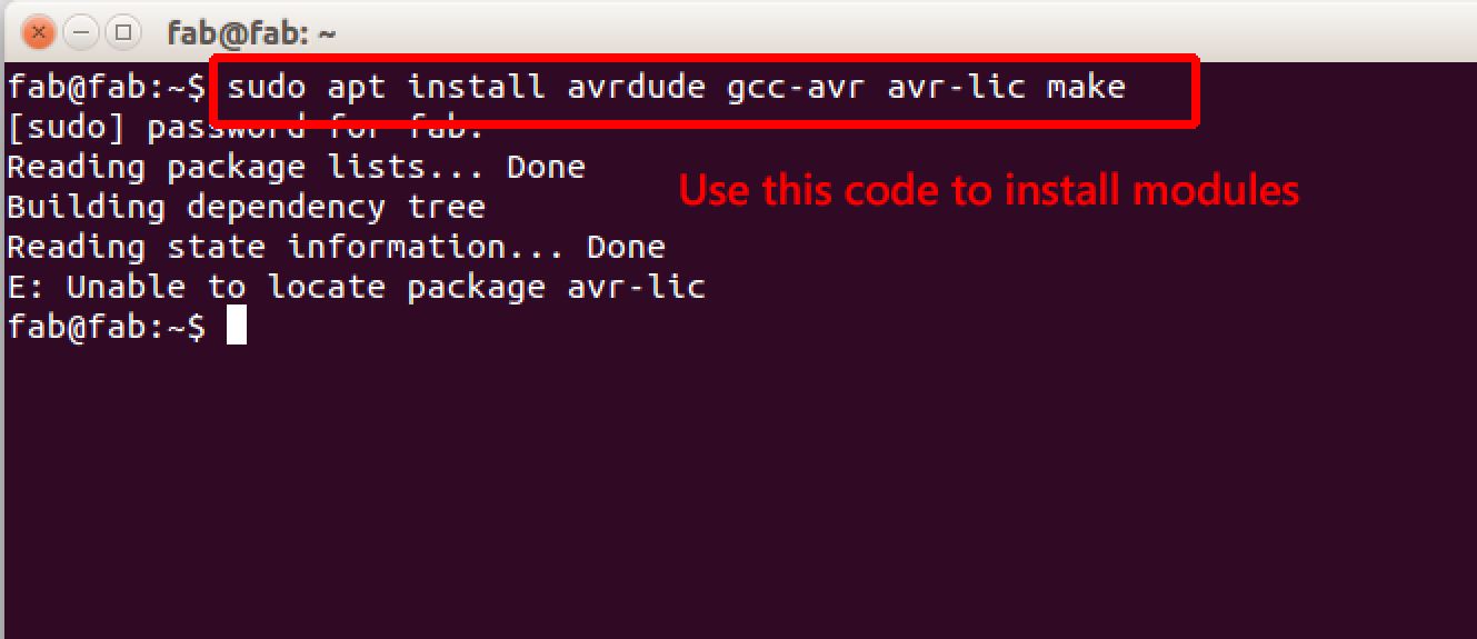
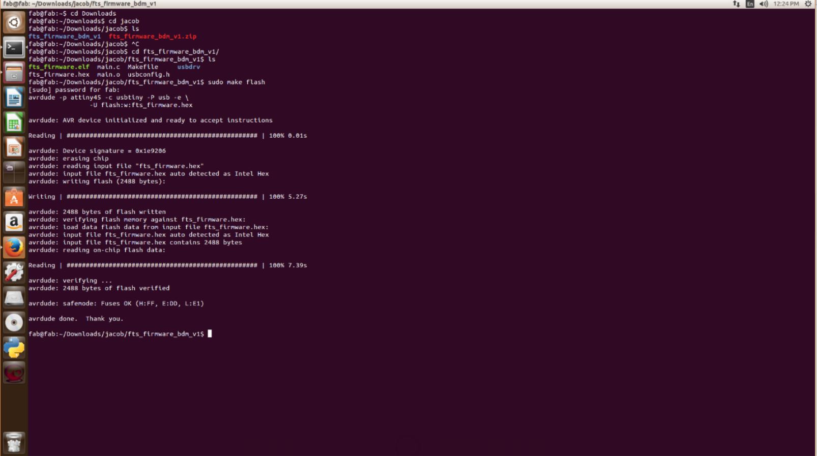
I also tried flashing my ISP this week.The required modules were installed on our Fablab PC.
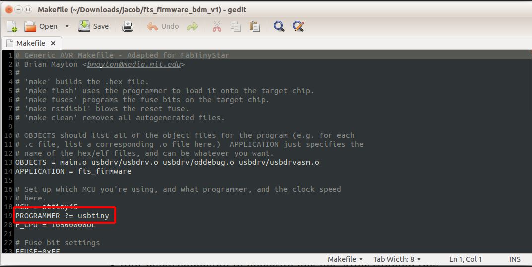
Now download the firmware and go to the firmware directory open the Makefile and check for USB tiny as Programmer.
Now use the make command to generate the hex file
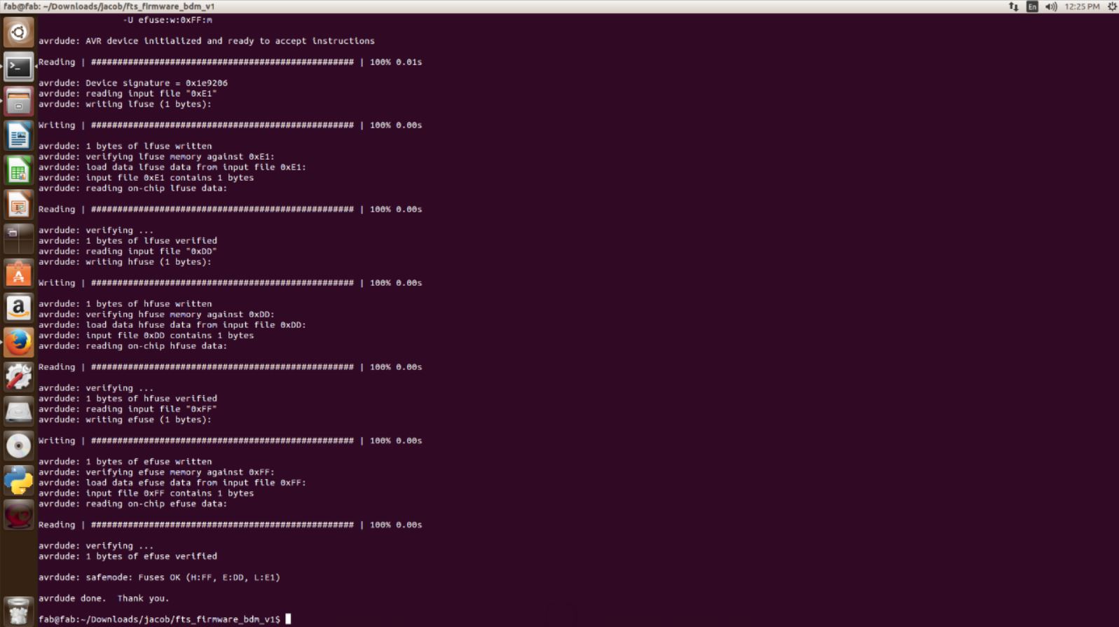
For burning the firmware into our ISP we used another programmer. The ISP is connected to the programmer using an IDC cable and it is then connected to the USB slot in PC. To flash the device all we had to do was to use two codes 'sudo make flash' and 'sudo make fuses'. I successfully burned the firmware into the ISP.
Testing
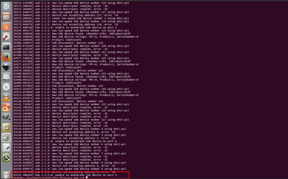
Now it was time to test my ISP. I connected it to the pc and the LED was turned on.To see the connected USB's I used the command 'lsusb'. But I couldn't find my USB tiny on the list. Then I used another command 'dmesg' to check the issues with my ISP. The system couldn't detect my ISP :(.
Trouble shooting
This was the part I was really scared of because finding the problem and troubleshooting seemed like a pretty difficult task to me. I tried flashing the device again. I checked the continuity and looked for any bridges or shorts in the circuits. But everything was correct including the connection. I just couldn't figure out what was wrong with my device. After checking for several hours I thought to see if I have misplaced any components. But I was pretty sure that I had all the right components. Going through the soldered components I found what the problem was. I have accidentally taken 49 K ohm instead of 49-ohm resistors. I immediately desoldered them and soldered in the 49-ohm resistors. I went through all the flashing process again and finally the PC detected my USB tiny. :D
Then it was time for some finishing touches.I used some hot glue at the top of the circuit to protect the circuit. I then used a file to have a nice flattened USB end. I also used a tape to increase the thickness at the end to ensure a perfect fit while inserting the USB.
To reset the reset pin I used a command sudo make rstdisbl.
Group Assignment
This weeks assignment was to characterize the specifications of our PCB production process.We mainly used 2 bits for our process a 1/32 and a 1/64. We checked the minimum resolution that each of these bits could process and we played around with the offset values also.
Using 1/64 bit

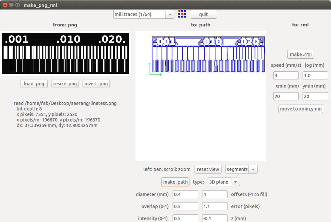
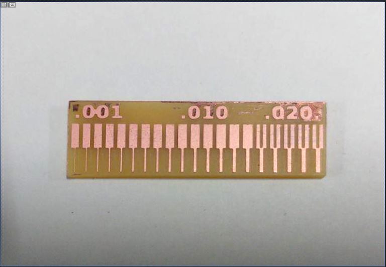
Some part of the copper was still left while using 4 as the offset value.
Using 1/32 bit
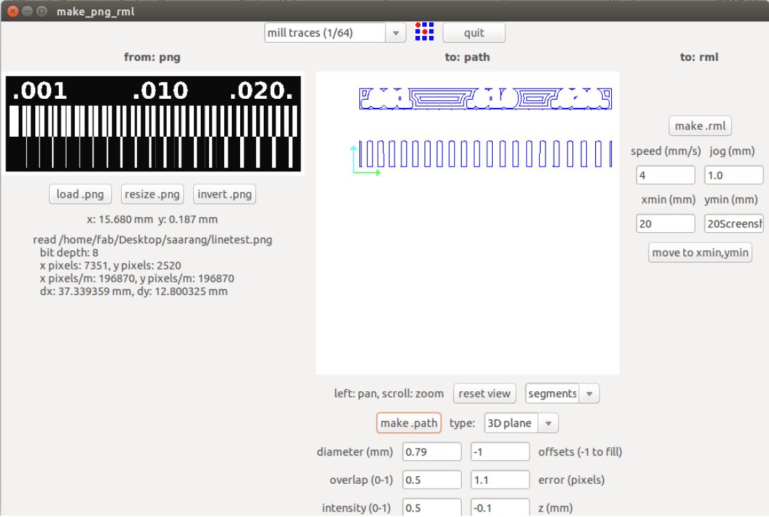
We used an offset value of '-1' here and we can clearly see that using a 1/32 bit couldn't process images in these resolutions.
