Electronics production
Characterize the specifications of your PCB production process - group assignment The team: Me, Kris, Isaac + support of Ilias.
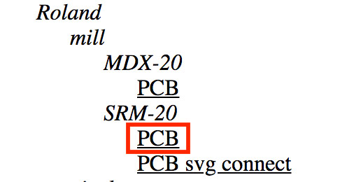
Characterising the machine
For millig the pcb board we are going to use Roland monoFab SRM-20 cnc milling machine. It’s suitable to mill Modeling Wax, Chemical Wood, Foam, Acrylic, Poly acetate, ABS, and PC board.
Workpiece table size is 232.2 (X) x 156.6 (Y) mm.
Distance From Collet Tip to Table is max. 130.75mm
Datasheet here
Machine comes with a controll software VPanel to regulate feed rate, spindle speed and position of X, Y, Z axes
To generate the toolpatch suitable for the machine you can use one of this programms:
- Mods It’s a node base programm, which is kind of better for learning and understanding the process. Each node represent the step like detecting outlines, calculating the patch based on parameters etc. Soyou can see “live” how the toolpath will change if you will modify parameter. It’s cool!
- FabModules It’s an older version of Mods. Hereyou can just see imput and output, without the process which is happening in between.
The material that we are going to use for milling the PCB boards is FR 1 plate. It’s a hard plate made from non conductive phenolic resin coated with thin layer of copper.
Generating Toolpaths with Mods
We are going to make a test with a design: http://academy.cba.mit.edu/classes/electronics_production/linetest.png

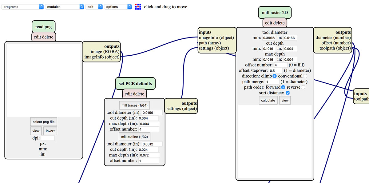
For converting the png file into rml format which is readable by the machine we are going to use the Mods programm: http://mods.cba.mit.edu/ it runs in a browser. In first step in Mods one has to open a server program for PCB milling with the Roland SRM-20.
In first node one have to choose the png with a pattern as an input file.
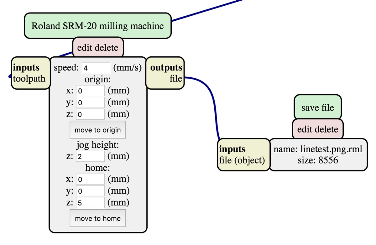
In the original Mods project file, the last node is the WebSocket device node. In our lab we prefer to use files. We replaced the WebSocket device with a save file node. The output from the Roland SRM-20 milling machine node has to be connected to the save file node.
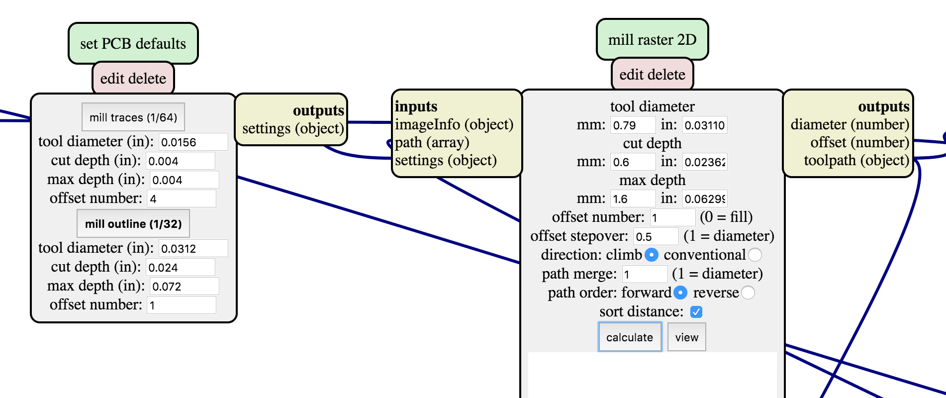
Next node is for Setting PCD defaults. It have two sections:
- mill traces 1⁄64 (<– drill bit size) - for milling the pattern on the board, it’s current png file.
- mill outlines 1⁄32 (<– drill bit size) - for cutting out the board from the plate - this will be second file.
In the node Roland SRM-20 milling machine we set all the origin coordinates (x, y and z) to 0mm, set the jog height to 2mm and home position to 0, 0, 5 (x, y and z respecitively).
We are going the set up the coordinates later manually, outside of Mods software.
Node The mill raster 2D is for setting up the tool properties. For the drill bit 1⁄64 the tool diameter will be 0.4mm, which is a rounded value of 1/64in. For the cut depth we have to specify how deep the tool will cut in one pass. In the case of cutting traces, 0.1mm is deep enough (max depth). After filling the values click calculate for generating the path for milling. Now we can save the file (in .rml format) in last node.
Setting up the machine
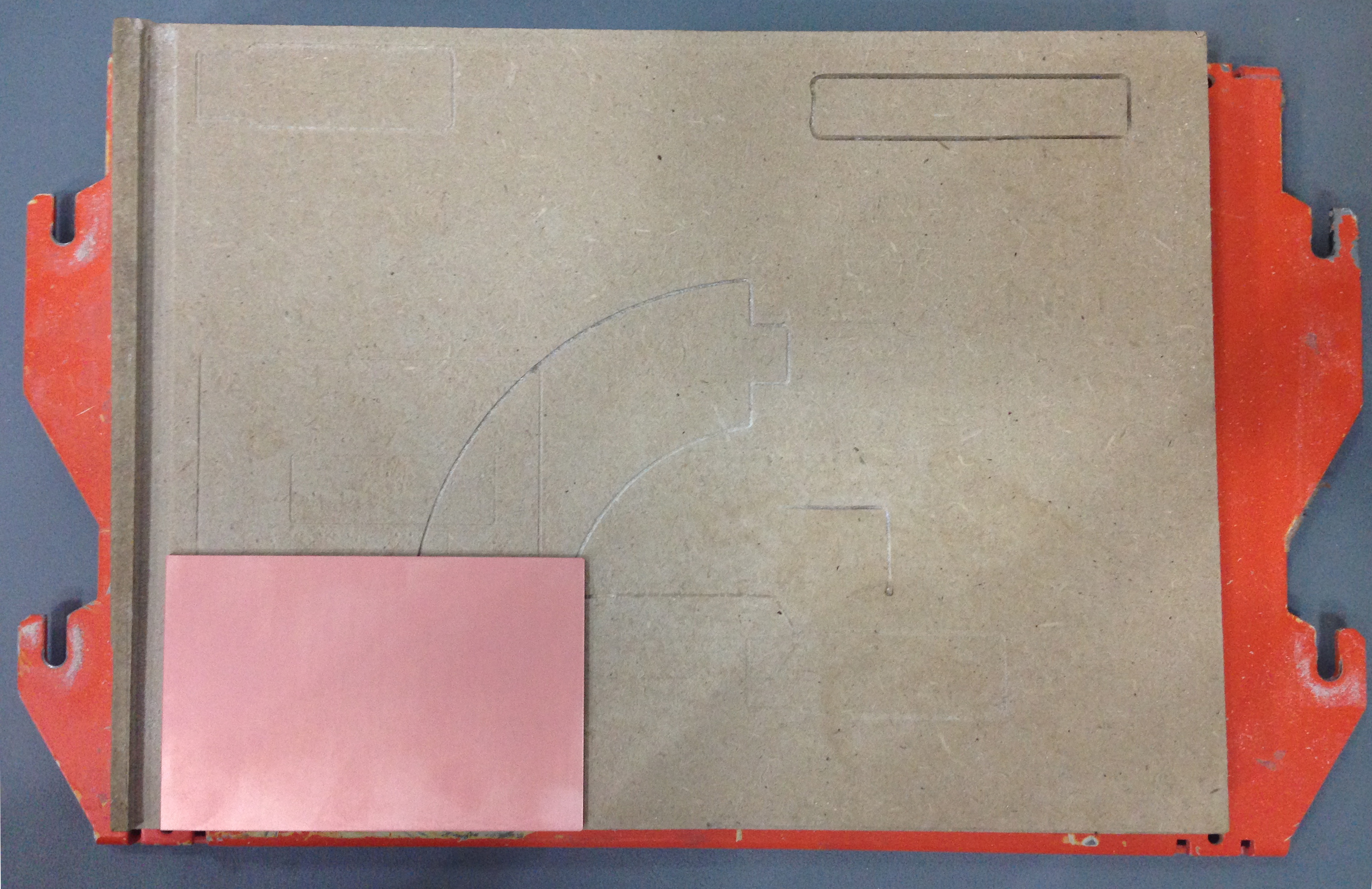
First thing we have to do is to fix the FR-1 copper-coated plate on the wooden plate on the machine (originally there is no wood on Roland, we have it here in fab lab barcelona). The 0,0 axis position is in down-left corner, we can put the plate there. We take the wooden plate out (unscrewing the screw which are responsible for keeping the plate in place) One have to be sure that the wooden plate is clean (one can clean it with alcohol 96%). On the back of the copper-caoted plate we put the strong double-side tape, than we press the plate strongly to the wood.
First we are going to mill the traces, thus we need to install the smaller drill - 1⁄64 (1⁄64 inches = 0.16 mil = ca. 0.4 mm).
Next step is to open the software for controlling the speed and drill position - Roland VPanel for SRM-20.
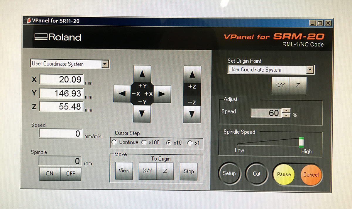
First we have to manually navigate to the bottom-left corner of our copper-coated plate and than press x/y in Set Origin Point section. This will set up the origin 0,0 in that point. For z axis we have to do it more manually. We go with the dlade down, but stopping few millimiters above the copper sufrace. Than we are loosing the drill (unscrewing the holder) and letting it drop to the plate. Than we are pressing the z in Set Origin Point section, to fix this position.
Next we lift the drill a bit up (by using the arrows in the Vpanel software) so it will start froma bit above, and than get to the surface.
In section speed we put 10%, so the process will start slowly. After a while we will increase it to 60% (manually).
To load the job we press Cut, than we delete previous job from the ist in fexist, and by pressing add we load our .rml file.
Next milling pass will be cutting out the board from the plate. Here the .png image that we are going to use.

We have to process the file in Mods and make a few adjustments:
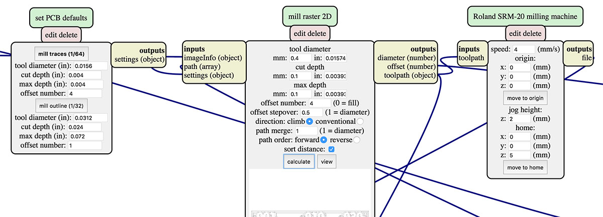
PCB defaults node: one has to hit the mill outline (1⁄32) button to load tool parameters for the 0.8mm diameter tool. Then we hit the calculate button in the mill raster 2D node to recalculate the toolpaths. We leave all the origin and home-related variables in the Roland SRM-20 milling machine node the same as for the tracing step.
Next we change the drill in the machine for 1/32 (1⁄32 inch = 0,32 mil = ca. 0.8 mm). We repeat the process of setting up the z-axis origin. The x/y stays the same as previously.
Again when everything is going fine with a speed 10% we can adjust it to 60%.
After all the cutting anm milling, we “tidy up” the dust by using a brush, and than we are removing the board. It’s good to start by lifting up one side with a wide cutter/blade or similar tool.
At the end is also good to clean the board by using a steel-wool.
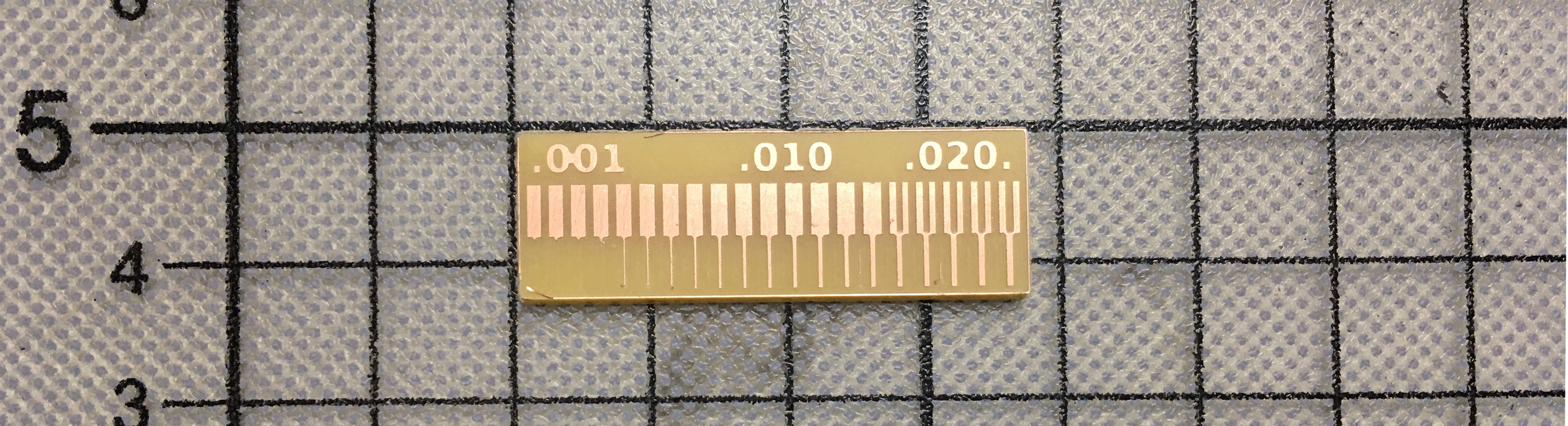
And here it is! The line thickness test in copper-coated board.
Lesson learnt:
- Looks like the line widths around .001mm are bit risky to mill, but thr ones nearer to .01 workvery well.
- When you are fitting the board with double-side tape to the wooden surface be sure to press it really strongly! Sometimes it’s a good practice to clean the wooden plate from rests of the previous tapes, or even hardly visible glue. You can do it with industrial alcohol.
Making an In-Circuit Programmer - individual assignment
We are going to create a board - ISP programmer, which will be able to programm other boards, so we don’t have to buy commercial programmers. That’s pretty cool that one can do it on it’s own.
I decided to follow the tutorial how to make FabTinyISP by Brian: http://fab.cba.mit.edu/classes/863.16/doc/projects/ftsmin/index.html
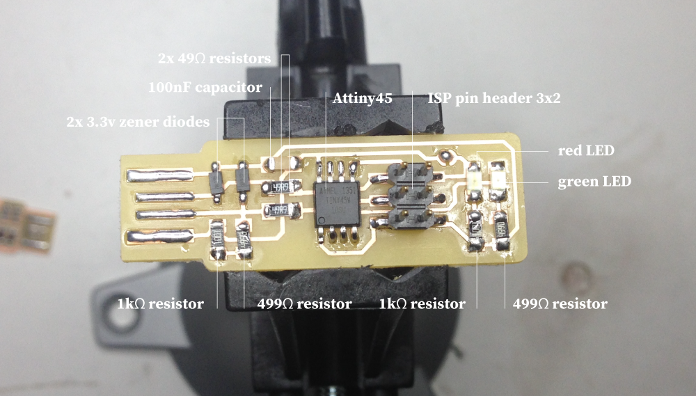
Below the schematic of the circuit and the .png files that I’m going to use.
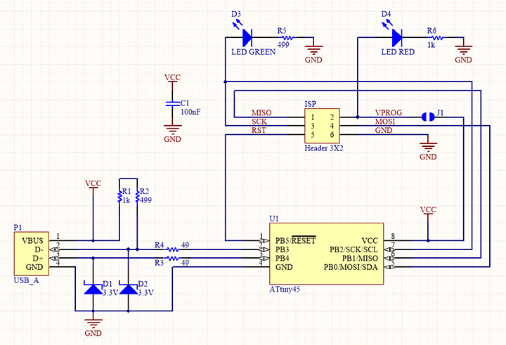

The components that I’m going to use are:
- 1x ATtiny45 or ATtiny85
- 2x 1kΩ resistors
- 2x 499Ω resistors
- 2x 49Ω resistors
- 2x 3.3v zener diodes
- 1x red LED
- 1x green LED
- 1x 100nF capacitor
- 1x 2x3 pin header
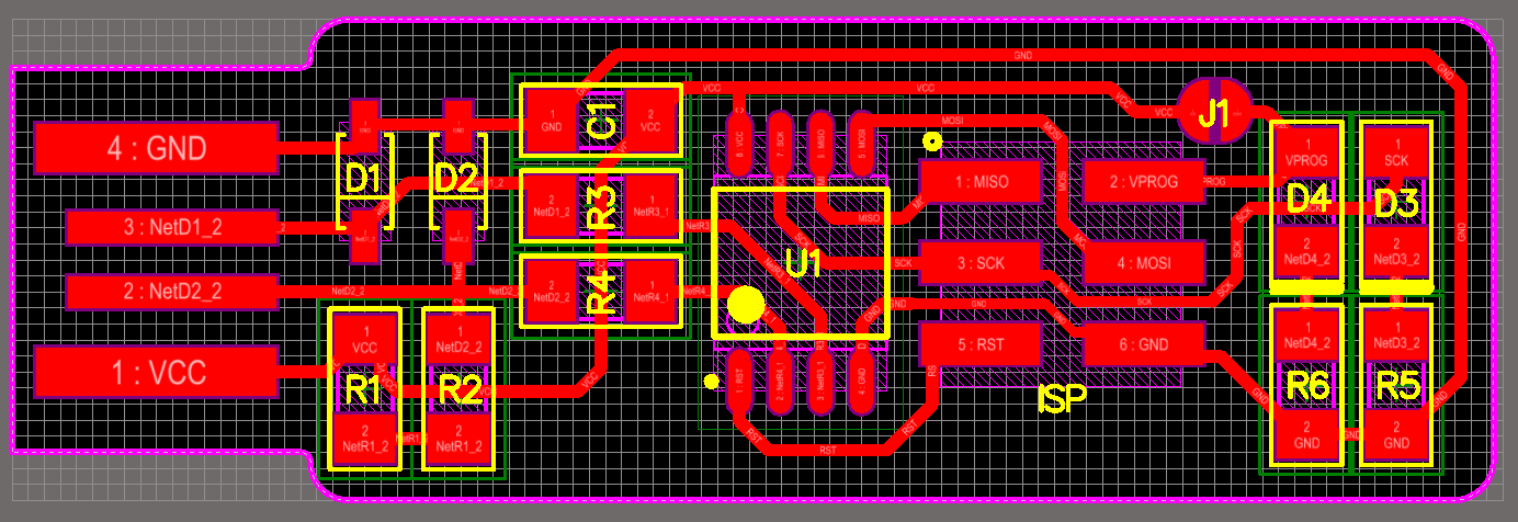
Using the wisdom gained in previous group task, I prepared the .rml files in mods, set up the proper drill, fixed the plate on the wooden board and started to mill…
Fail! looks like the plate was not properly fixed on the wood (though I used the double tape)…maybe I didn’t press enough one surface to another. The plate moved and everything was screwed up.
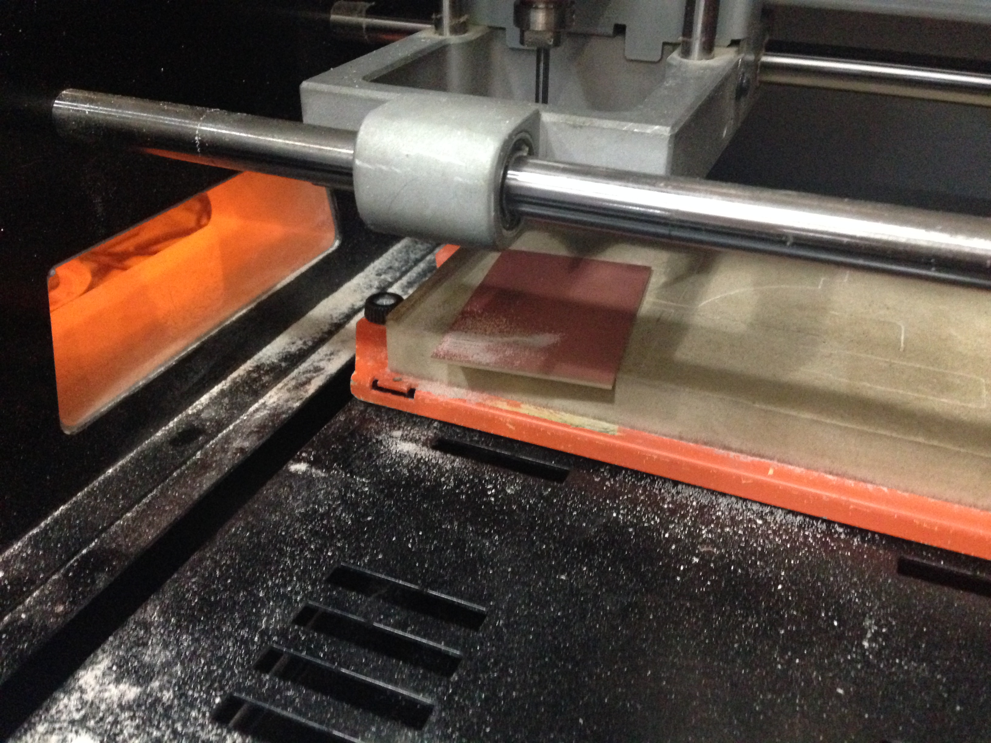
Next time it went better. I’ve managed to mill and cut everything properly.
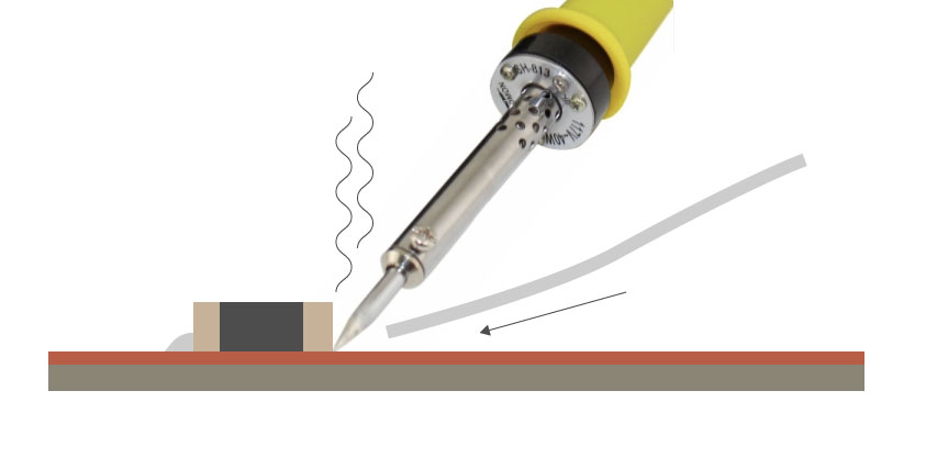
After gathering the components the time has come for soldering. I practiced a bit before so it went pretty smooth. Thanks god there is always an option to unsolder or readjust the components.
While putting the components on the lace one has to pay attention for the orientation of some of them. Also there few important tipps in the tutorial whico component solder as first and last:
- first put the ATtiny45, since is the most difficult
- the zener diodes have a line-mark on cathode side
- the LED cathodes on the PCB drawing are marked with dots and thicker lines
- the ATtiny45 marks pin 1 with a dot laser-etched into the corner of the package. Pin 1 is marked in the drawing also with a dot.
- 1x 2x3 pin header put as last
Another important thing was to create a temporary solder-bridge, which could be removed after programming the microcontroller (marked as J1 in the red schematic above).
Soldering
While soldering is great to have a good direct light and a magnifying glass fixed to the table lamp.
After soldeing some components I realised that the best order of steps is:
- fix the board or in clamps or just tape it with double-side tape to the table
- clean it with alcohol to remowe the grease from fingers
- make small drop of the solder on the right spot
- heat it up again and put one side of component there
- for other side put the soldering iron on the connection of the other side of the component and board to heat them both
- stick the soldering wire on the connecting spot to get a nice bubble of solder
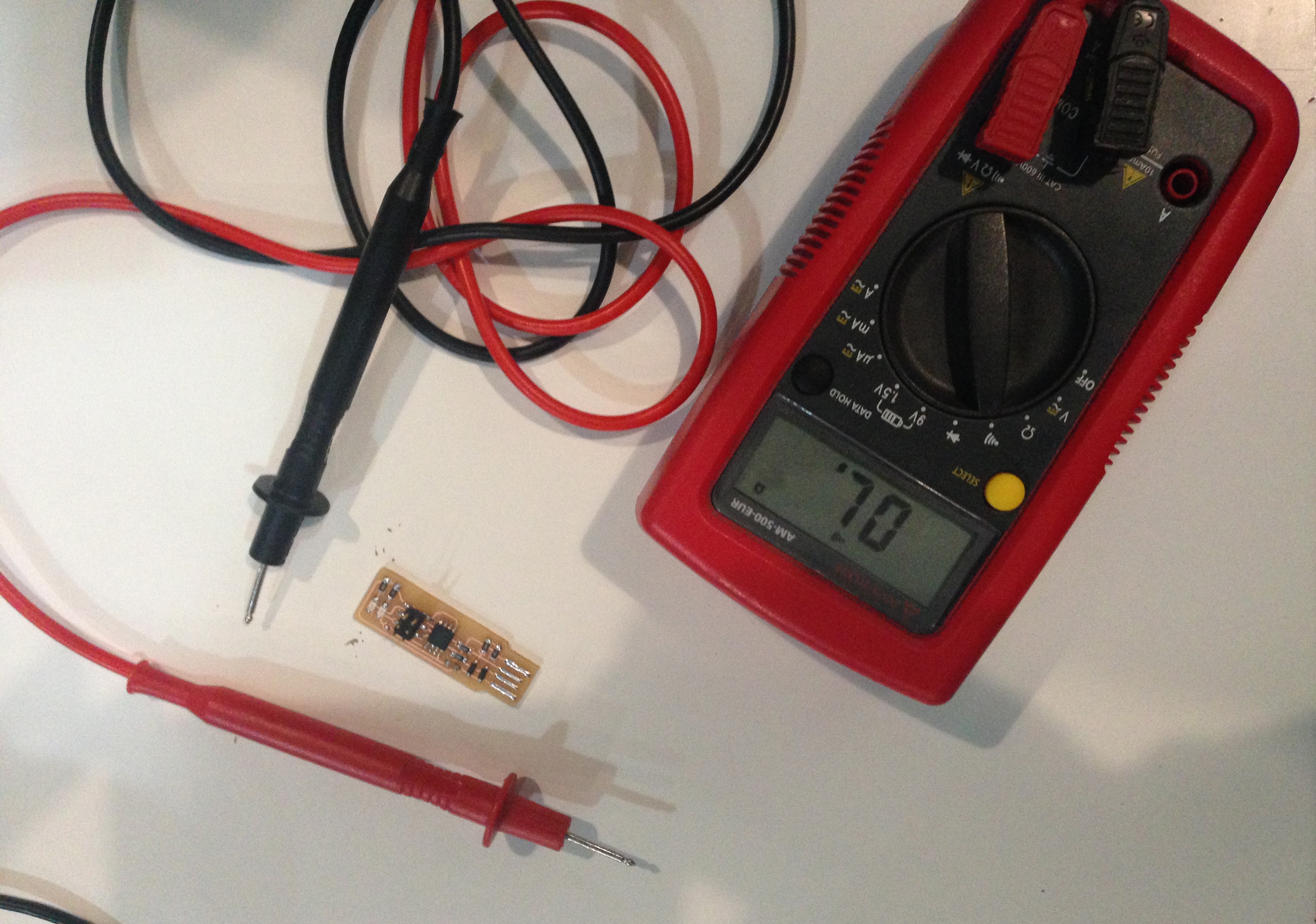
YEAH! I’ve made a test with multimeter, and seems like everything is working!
Programming the programmer
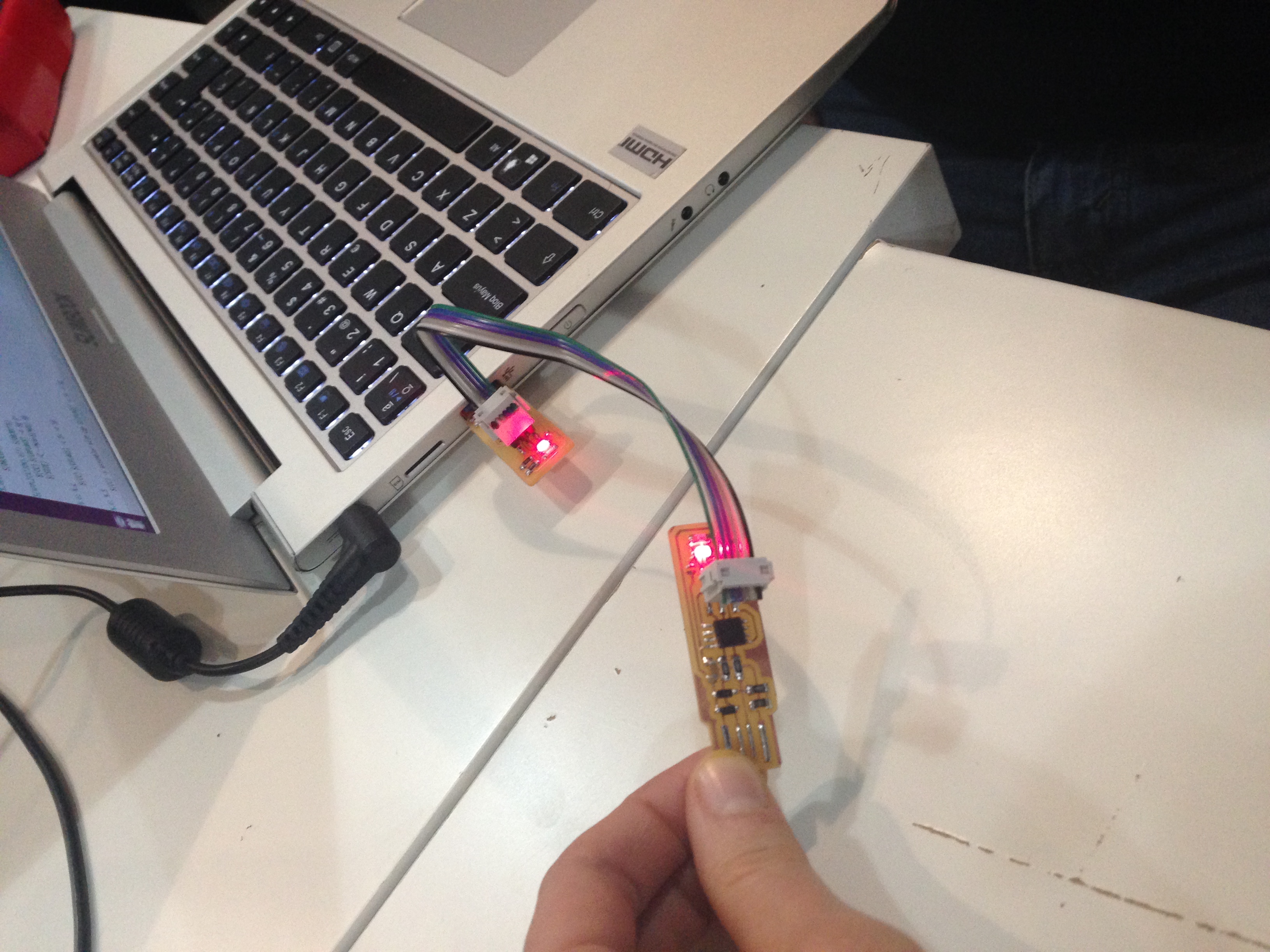
I wanted to try to programm my programmer with programmer of Kris (which was already programmed before). But there a problem occurs. When we’ve been plugging both programmers (one after another) to the laptop usb to check if computer is recognising them…it didn’t worked out. There was a connection (since the red LED was on) but computer couldn’t read the data.
There is a command dmesg to see all the actions being processed by computer in current moment. We can see there if our device is recognised, and what is the problem.
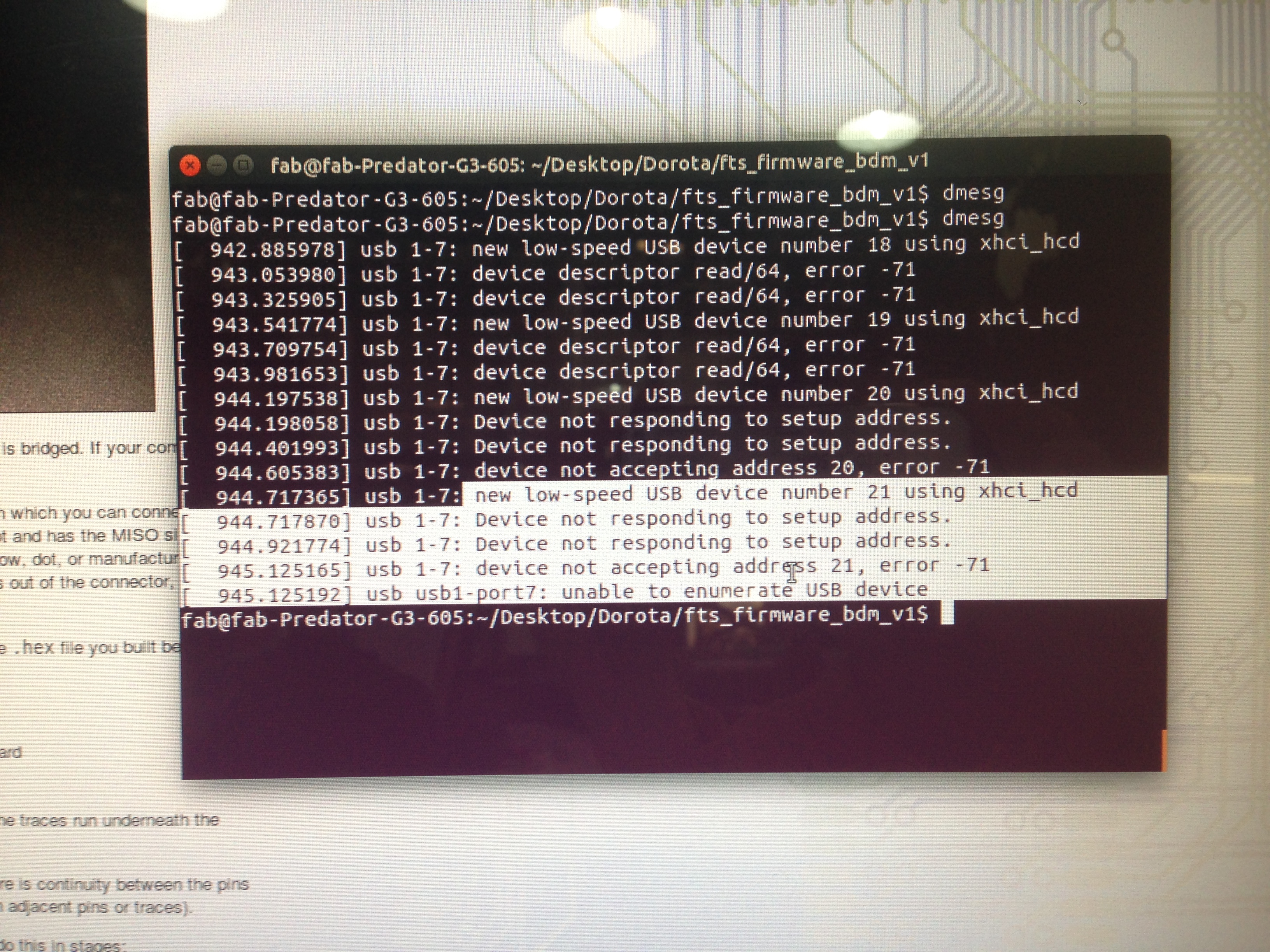
I got good hint from tutor that it could be becouse of too small amount of solder on the side of one component (capacitor)…and it was that! After adding a drop my small programmer was recognised!
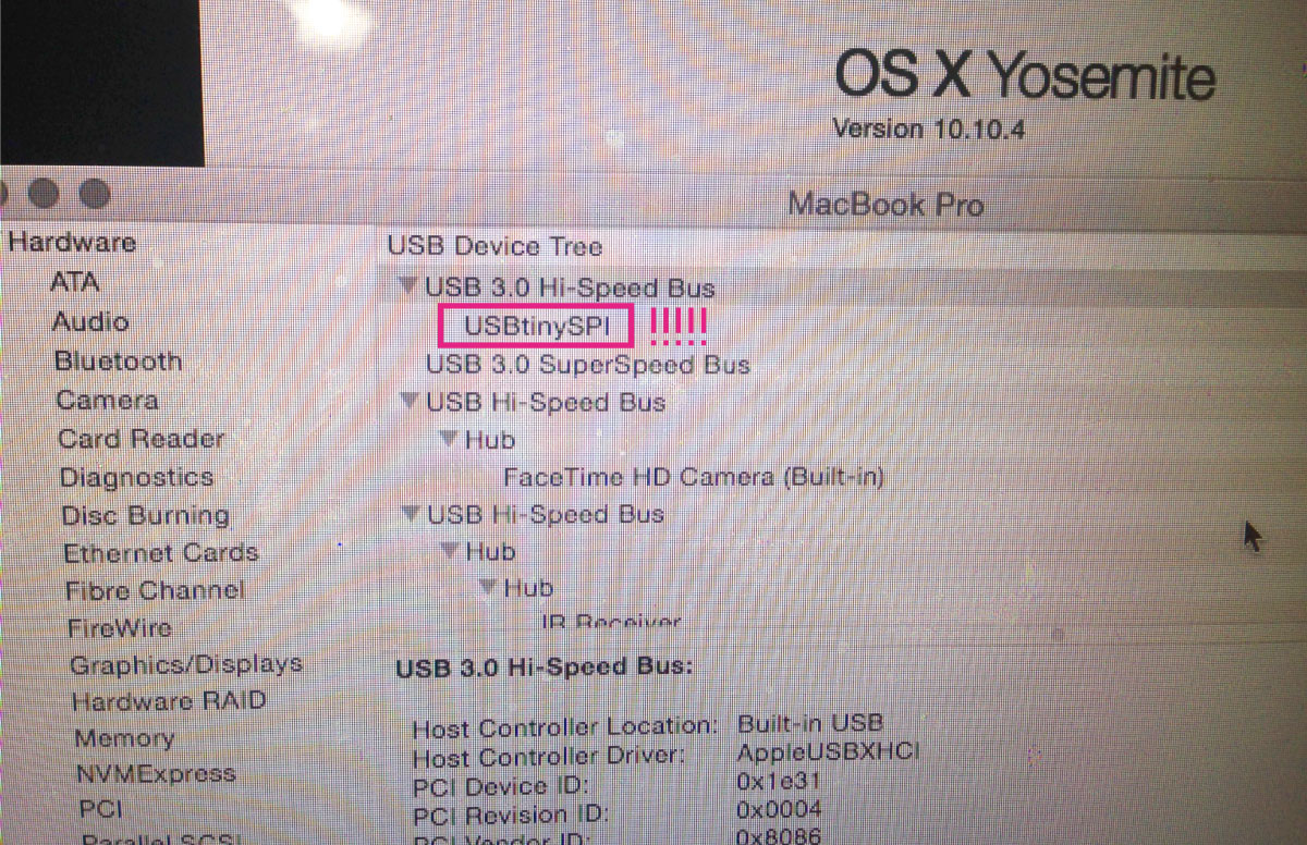
One can check it be going to About this Mac > System Report > USB (from the left list), it USBtinySPI should be listed there.
Now we can programm the programmer by using the commercial AVRISP2.
- download CrossPack AVR (
AVRis a family of microcontrollers) to set up a development environment: https://www.obdev.at/products/crosspack/index.html. The programms will be put in/usr/local/CrossPack-AVR/bin. - download the fts_firmware_bdm_v1 source code, unpack in proper location and navigate to in in command line (
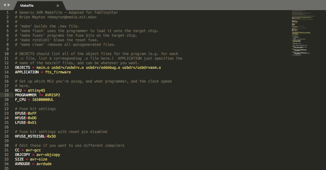
cd). - modify
makefilefile from firmware by using Sublime. Near the top of the file, find the line that says:PROGRAMMER ?= usbtinyand change usbtiny to whatever programmer you’re using.
- type the command
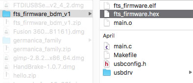
make- to compile the source code and get the filefts_firmware.hex(willbe created in the firmware folder). Now we are going to flash this firmware on our programmer/board
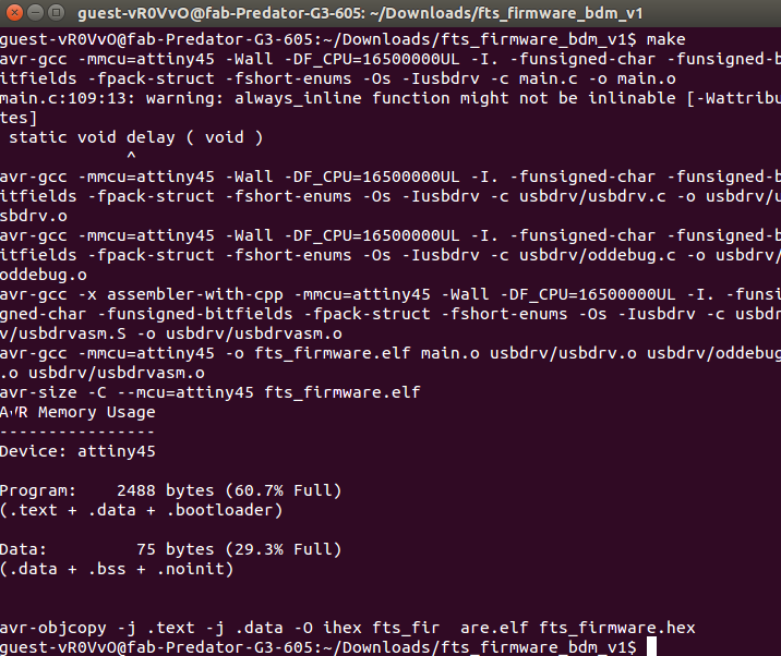
SCREENSHOT FROM FAB COMPUTER MAKE
- plug the board into USB port, plug the ISP header to the port at the end of the cable of AVRISP2 programmer. The red light on your board and green on the AVRISP2 programmer should be lighted up.
- run ‘sudo make flash’ in the terminal - to erase the target chip and program the flash memeory with the content of
.hexfile
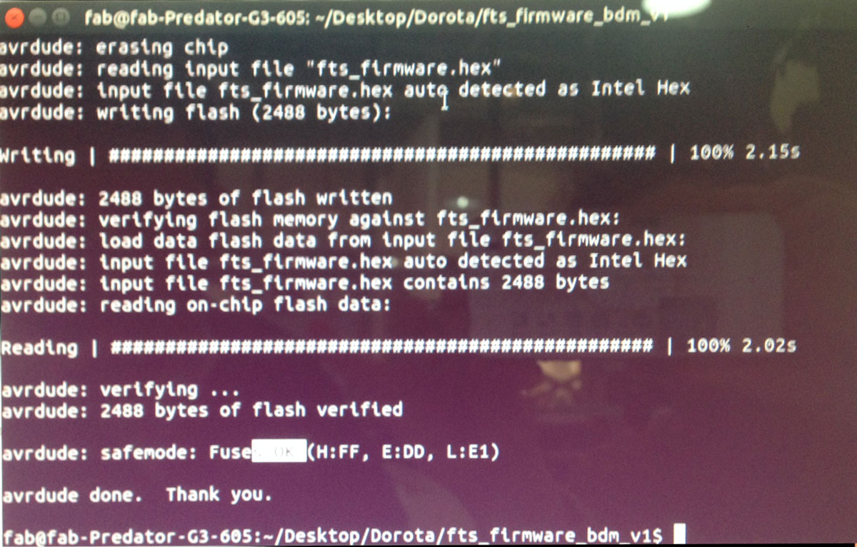
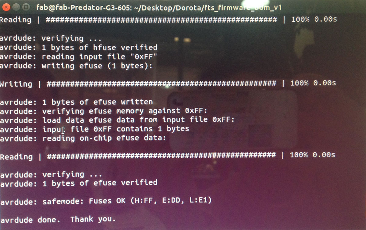
- run
sudo make fuses- this will set up the microchip to work
- remove the bridge on the solder jumper (
J1)
THATS ALL FALKS!