Electronics production
Group assignment
Fabio has a nice description of our PCB milling machine on its website.
3D printed board
As an electrical engineer, I make PCB for more than 20 years.
When I started designing PCBs, my department was using chemical etching.
10 years ago, we acquired a PCB milling machine.
Nowadays, we mainly outsource our PCBs.
With this experience, I decided to try something new: 3D printed PCB.
I saw several videos of people using a 3D-printer to make PCBs.
I decide to try a method using copper foil tape on 3D print board.
Design procedure
KiCAD
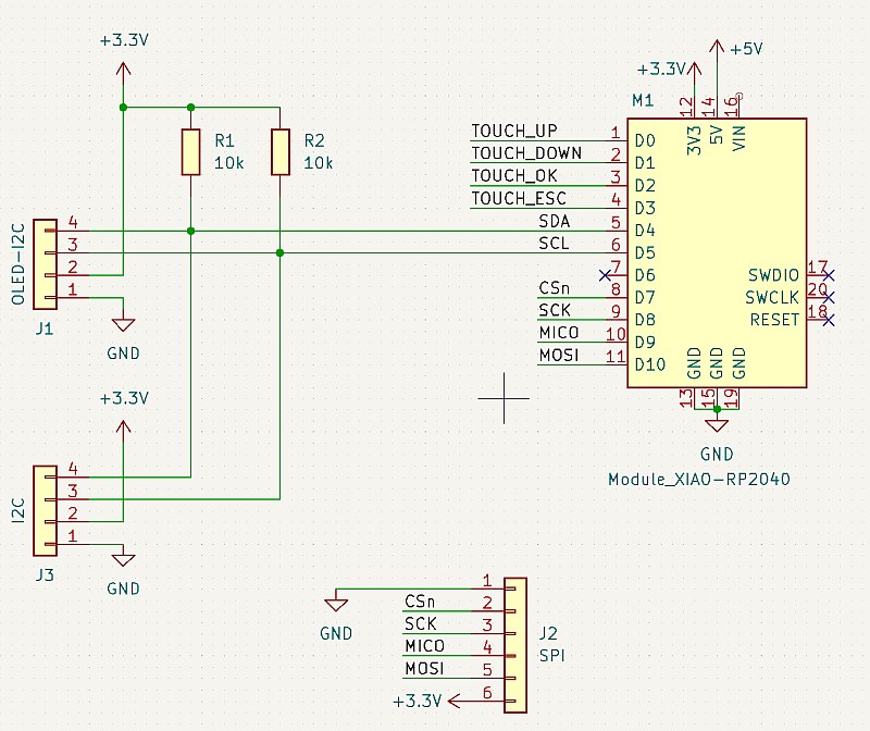
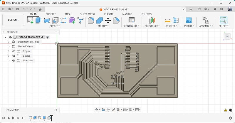
First step is to design the PCB. I used KiCAD to make a simple board, inspired by the QPAD:
Next, use File/Plot... to export the PCB as a svg file:
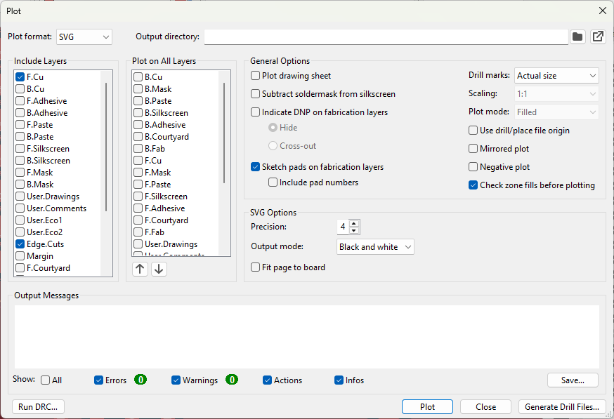
- Uncheck Plot drawing sheet, we don't need it
- Select Actual Size for Drill marks, to have the correct size for the holes
- Check Sketch pads on fabrication layers to add the holes on the edge-cuts layer
- Click on Plot
Fusion360
I'll use Fusion360 to create a 3D pcb from the svg files.
It'll be 2 mm thick in total.
The copper traces'll be engraved in it with a depth of 0.2 mm (a 3D printer's layer thickness).
After some tests, I found out that it's easier to extrude the contour of the copper traces.
Creating a pocket for a copper trace is a long process as it's made of several profiles that has to be selected manually.
Usually, in a PCB, there are less non-copper non-contiguous surfaces than copper traces.
It's now time to import the svg file in Fusion360:
- Create a new file
- Create a new sketch, select the horizontal plane
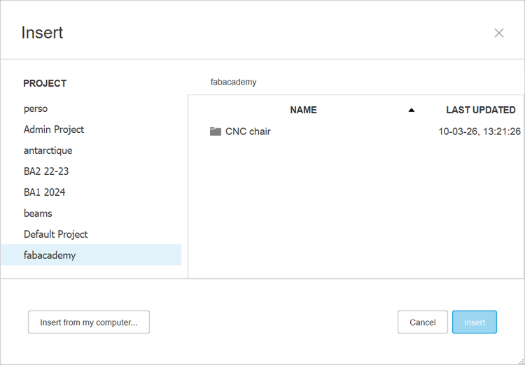
- In the sketch toolbar, select Insert/Insert SVG
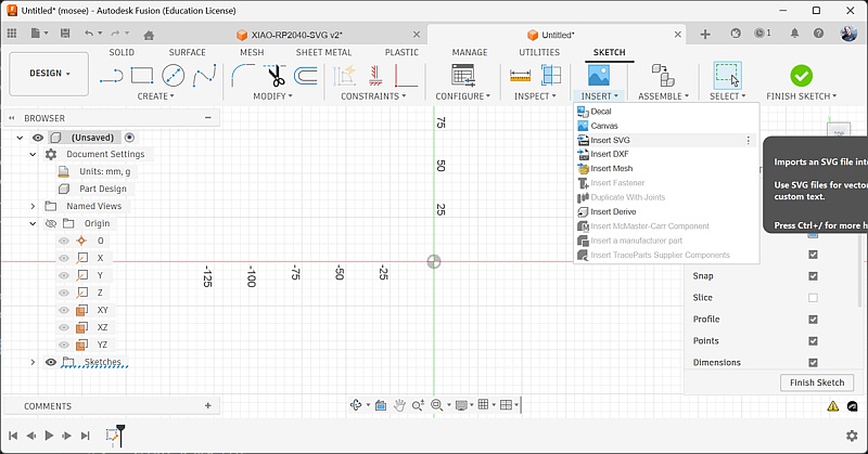
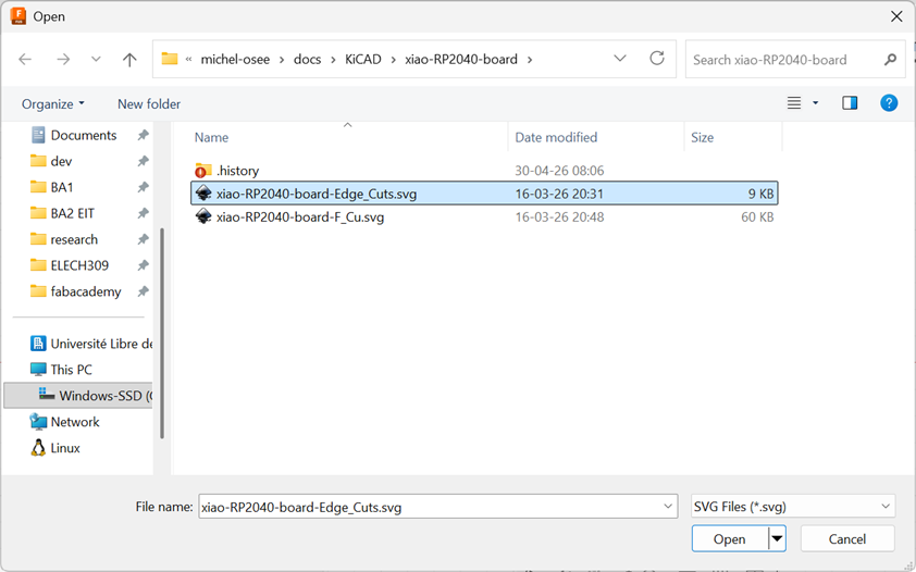
- In the dialog window, select Insert from my computer...
- Select the edge-cuts svg file, created with KiCAD
- There is no need to place the sketch at a particular position, just click OK
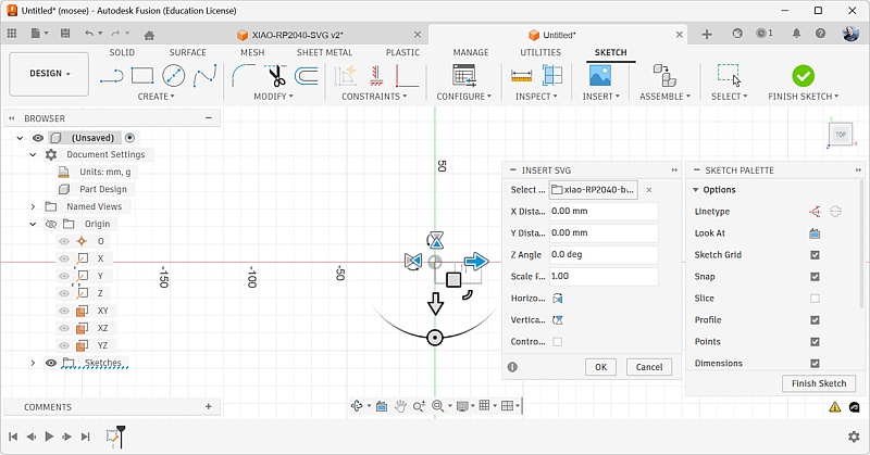
- Click on Finish sketch
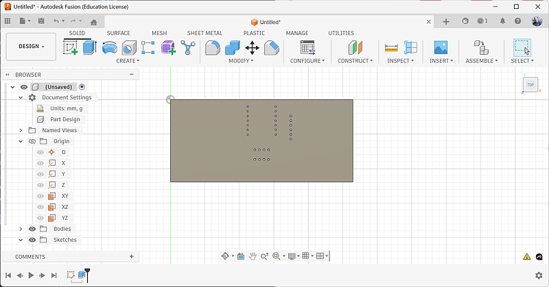
- In the Solid toolbar, select Extrude. Click inside the sketch to select the profile to extrude and choose a distance of 1.8 mm
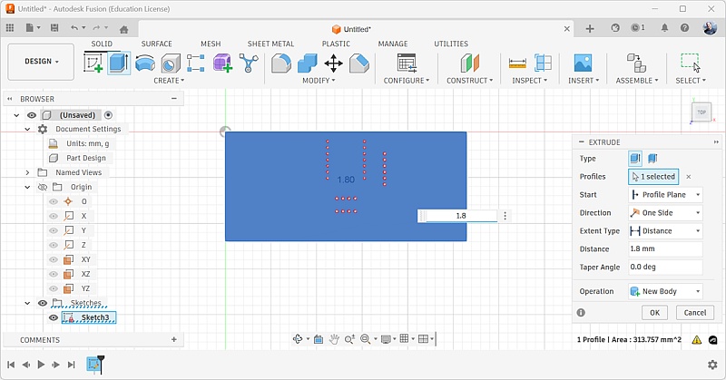
- Results should look like this
- Create a second sketch and select the top face of the first extrusion as its plane
- The svg appears rotated in my sketch:
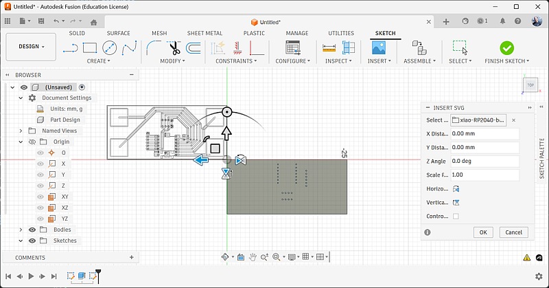
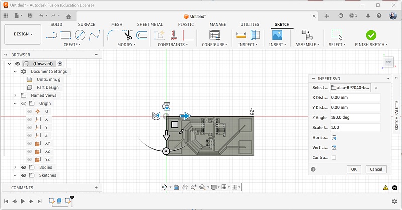
It could happen, depending on how Fusion360 choose the X and Y axis orientation
- in that case, change the Z angle to 180°
-
Finish the sketch
-
Create a new extrusion
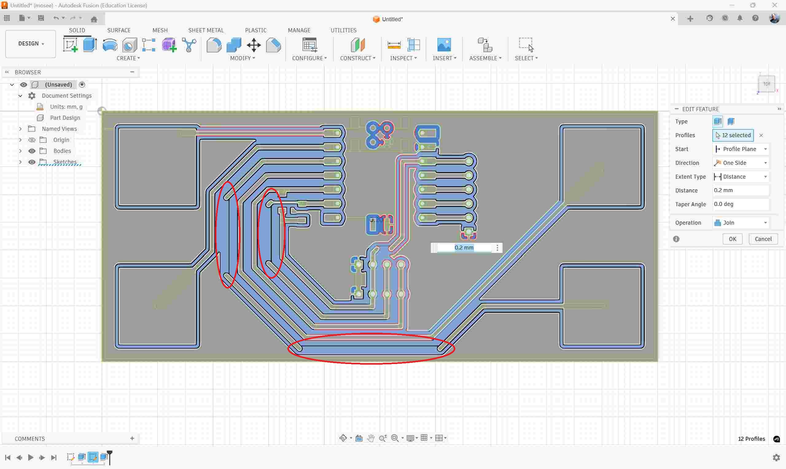
When I tried to select the profiles to extrude, I realize that there are errors in my sketch.
It seems that KiCAD drew some of the copper traces without any thickness, as simple lines.
As they are not closed profiles, Fusion360 can't extrude the sketch.
I opened the svg file in Inkscape to see if I can repair it
In Inkscape, everything looks normal.
After some trials, I found a workaround:
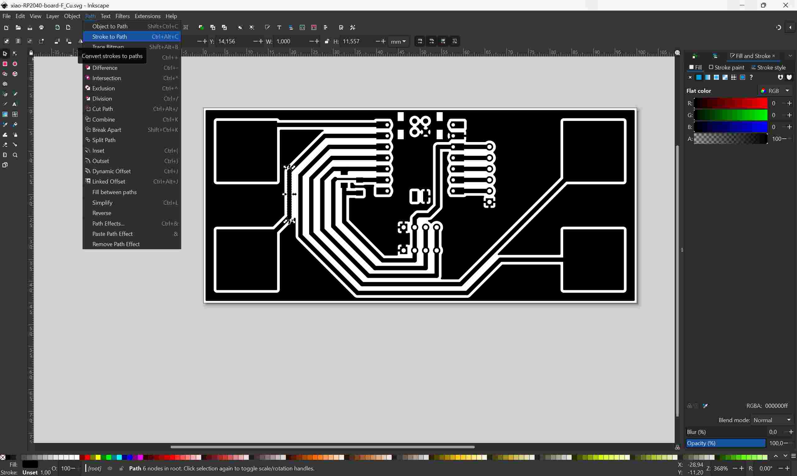
- Select the faulty track
- in the Path menu, select Stroke to Path
It creates a path on the edges of the selected object
I imported the updated svg in Fusion360
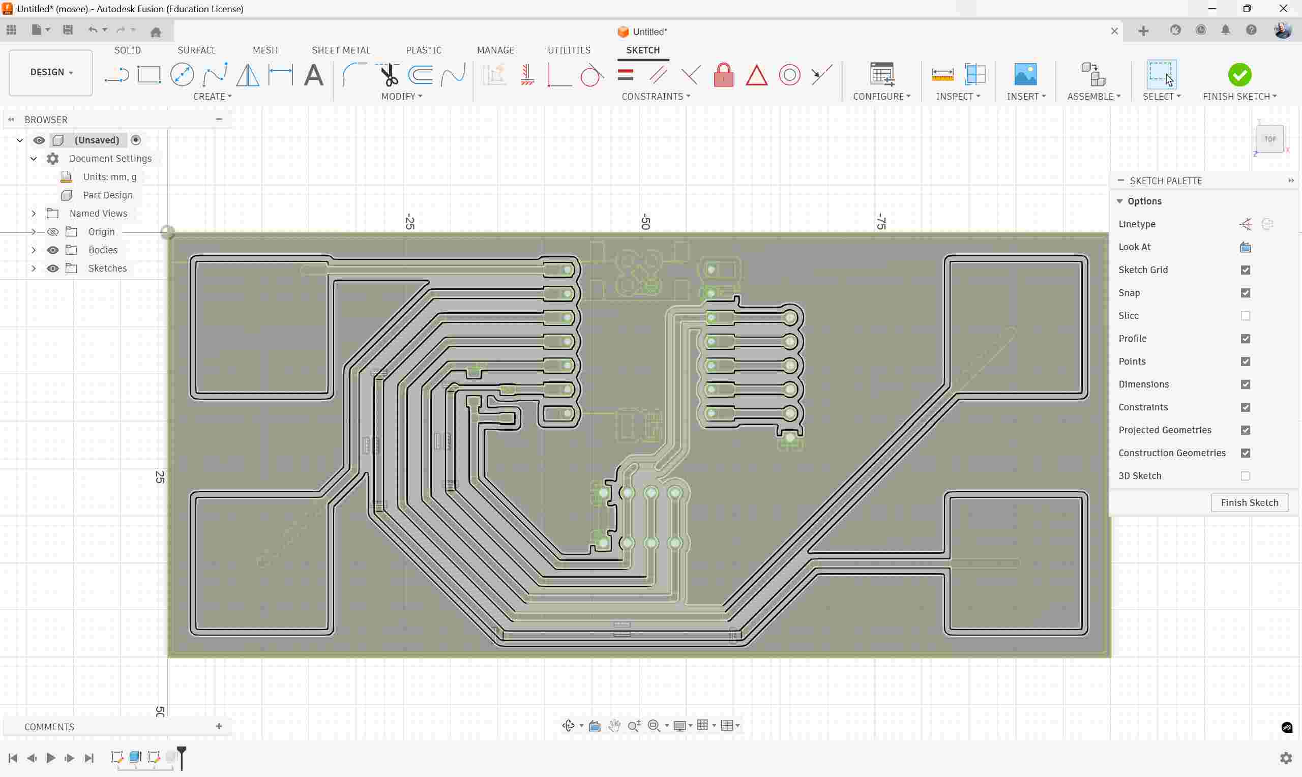
The new paths can be seen on the sketch.
- Create a new extrusion
- Select all the surfaces that are not copper traces
- Check that the selected operation is Join
- Choose a distance of 0.2 mm
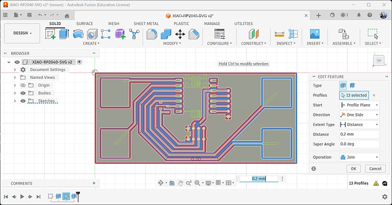
I added a 1 mm fillet on the four corners: I don't like sharp corners on PCB
Manufacturing
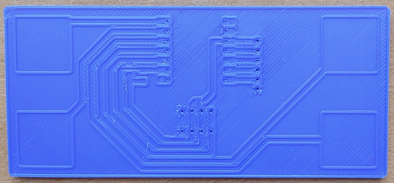
I exported my PCB as a step file to print it with a fab lab's 3D printer:
Next, I put a sticky copper foil on the 3D-printed board
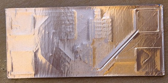
I used my finger nail to press the foil and make it wrap around the extrusions defining the copper traces' edges
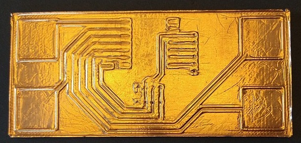
It's time to start sanding!
I used a fine sand paper (240). I placed it flat on a table and rub the pcb on it.
It ensures that I only sand the copper on top of the extrusions.
The progress was very small and I got frustrated.
I decided to try sanding the usual way: rubbing the sand paper on the pcb.
Progress speed improved drastically, as I was able to concentrate on each copper trace individually.
I found out that the copper foil is thick and strong enough to ensure that I won't damage a copper trace during sanding.
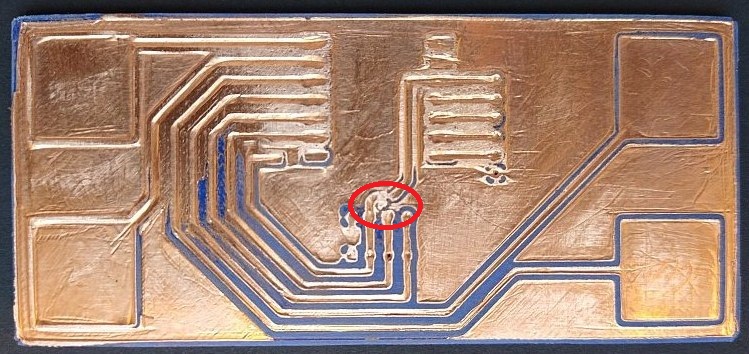
However, I was proven wrong as I started to peel off a copper trace in the center of the PCB, where it has a sharp turn around another trace.
I put it back in place and add a bit of solder to reinforce it.
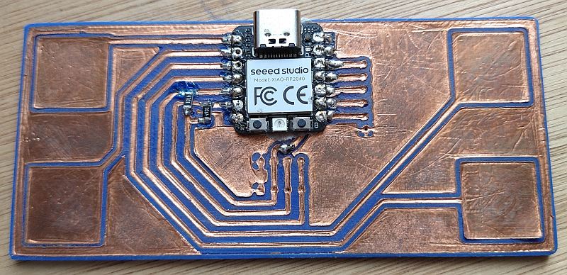
Final result looks good:
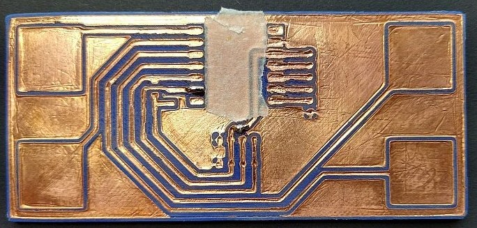
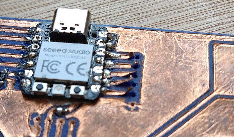
As the picture shows, I added a masking tape piece below the Xiao to avoid short-circuit with the ground plane
PCB testing
As I always do, I started by checking continuity of all copper traces with a multimeter.
I also check for short-circuit between traces.
Everything was OK. I expected that as the circuit is fairly simple and the traces are 1 mm wide.
Soldering 1
I was curious about soldering on a PLA substrate, but it went without any problem.
I started with the Xiao and didn't find it different compared to soldering on FR2 or FR4.
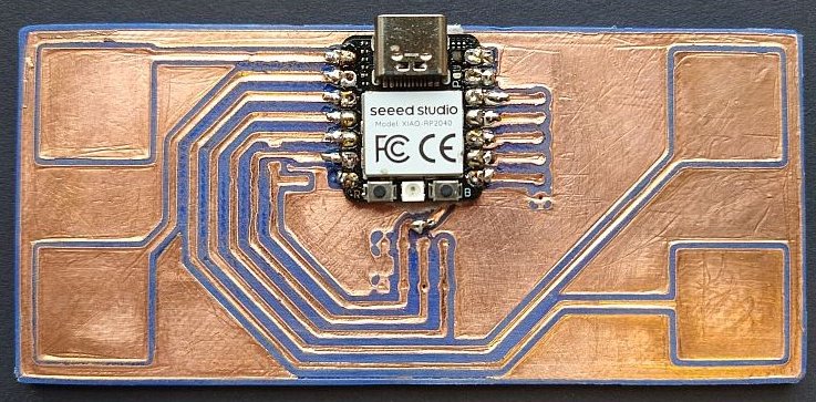
Next I soldered the pull-up resistor for the I2C:
I struggled a bit with one of them and heated the PLA too much.
The result is not pretty, but still functional.
When I finished soldering the SMD components, I decided to test my circuit with Neil's code example for capacitive touch.
Test
I downloaded Neil's code example for capacitive touch.
The only modification I had to make is changing the pins' ID, as i didn't use the same pins.
The modified code can be found here.
I had the same result as Neil, but unfortunately, I forgot to take a video.
Next day, I wanted to redo the test to have a video and my PC didn't recognize it.
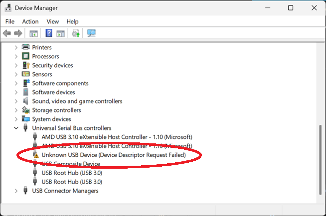 .
.
I checked if there was any short-circuits between the Xiao's pins, but didn't find any.
As I didn't make any change during the two tests, I don't know what caused this malfunction.
Soldering 2
Next, I wanted to solder the LCD header, but I had a problem: the holes were too small. I forgot that 3D-printed holes are usually smaller than expected.
Trying to drill them bigger peeled off the copper traces around them:
Lessons learned
- This method works better than I expected.
- The sanding part is a bit tedious, but not difficult.
- Soldering on PLA is not a problem, but requires some skills
- Avoid trough-hole components
- If needed, be sure to draw bigger holes than needed, or verify and correct their size before applying the copper foil
- Use SMD connectors
- The copper foil adhesion is good, but applying a varnish is probably a good idea to improve long term mechanical stability
- I don't think it's better than FR2 milled PCBs.
I would reserve this technique for special applications like non planar circuits.