Electronics Production
Group assignment:-
Characterize the design rules for your in-house PCB production process: document feeds, speeds, plunge rate, depth of cut (traces and outline) and tooling.
-
Document your work to the group work page and reflect on your individual page what you learned
Individual assignment:Machine:- DGSHAPE monoFab SRM-20
- Cuttable Material: Modeling Wax, Chemical Wood, Foam, Acrylic, Poly acetate, ABS, PC board
- Operating Speed:  0.24 – 70.87 inch/min (6 – 1800 mm/min)
- Spindle Rotation Speed:  Adjustable 3,000 – 7,000 rpm
- Mechanical Resolution:  0.0000393 inches/step (0.000998594 mm/step)
- Control Command Sets: RML-1, NC code
Characterize the design rules for your in-house PCB production process
I started with the trace width line test. Toolpaths were generated using MODS CE.
I used the default settings in MODS excepts for the following minor changes.
Under "Roland SRM-20 Absolute coordinates":
origin: x,y,z  = 0,0,0 (mm)
home: x,y,z  = 0,0,5 (mm)
Setting the Z home to 5 mm above the material will prevent damage to the tool if the gantry was ever moved to the home position.
The settings below, with the exception of speeds, are part of the MODS defaults and produced consistent results for PCB milling on our monoFab SRM-20. The results can be seen here.
Feeds
- 4 mm/s
Speeds
- 7000 rpm
Plunge rate
- This was hard coded in MODS CE at 10 mm/s
Depth of cut (traces and outline):
 - traces: 0.1016 mm / 0.004 in
 - outline: 0.6096 mm / 0.024 in
Tooling
- 1/64 mill: 0.39624 mm / 0.0156 in
- 1/32 mill: 0.79248 mm / 0.0312 in
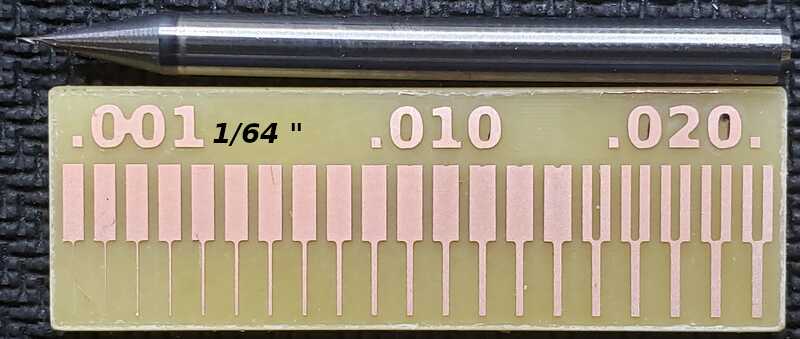
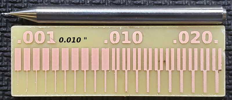
Trace width line test
1/64" end mill
- The thinnest gap a 1/64" end mill can mill into is 0.016".
- The thinnest trace a 1/64" end mill can mill satisfactorily is 0.004".
0.010" end mill
- The thinnest gap a 0.010" end mill can mill into is 0.011".
- The thinnest trace I'd feel comfortable with using a 0.010" end mill is the 0.003".
Document your work to the group work page and reflect on your individual page what you learned
Feeds, speeds, plunge rate, depth of cut and tooling will vary depending on the characterization of the machine, the tools, the materials used, and the desired outcome. Understanding of what the machine can do, it's limitations and the quality of work it can perform informs the user of how to best design for the desired outcome. This information and it's appropriate application can also extend the life of the tool and the machine. It's also useful in recognizing and troubleshooting problems that may arise. For any new materials or tools used, this characterization needs to be performed again so nominal values and settings are established for good, consistent results.
Make and test the development board that you designed
- Described the process of milling, stuffing, de-bugging and programming
- Demonstrate correct workflows and identify areas for improvement if required
Milling
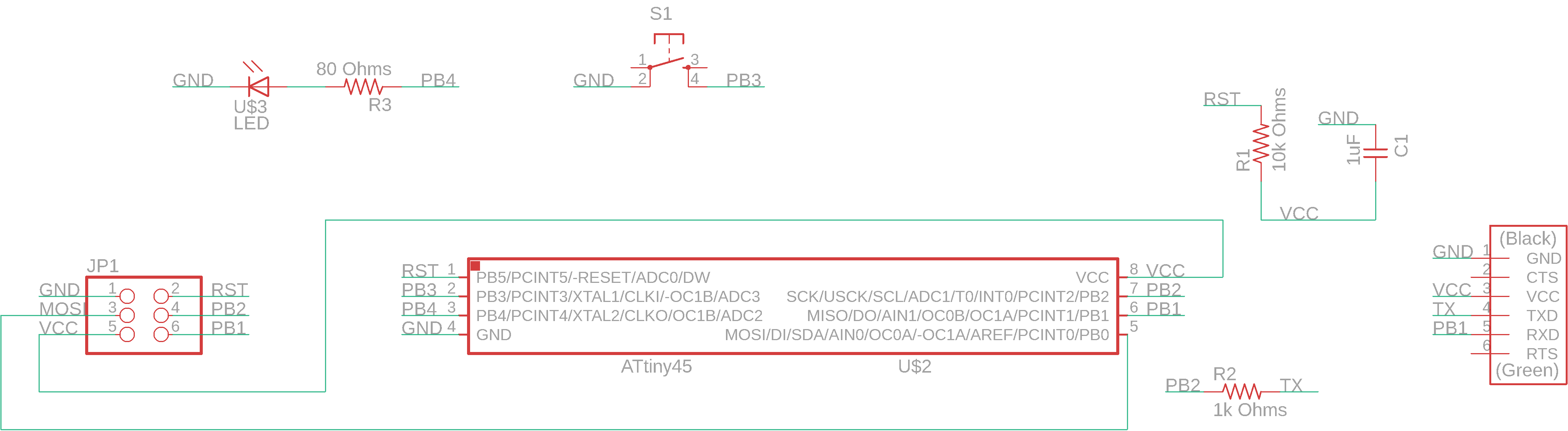
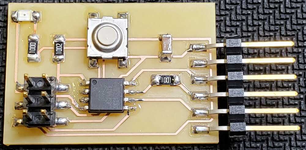
Using the circuit produced in Electronics Design:
Concept:
Using a serial connection to the board, type out a message and push the button to have it blink out the message using morse code.
Components List:
- 1 x ATtiny45
- 1 x 1 kΩ resistors
- 1 x 100 Ω resistors
- 1 x 10 kΩ resistors
- 1 x 1µF capacitor
- 1 x LED
- 1 x ftdi connector
- 1 x (2x3) pins
- 1 x B3SN-3112P tactile switch S
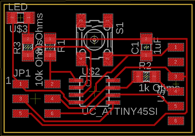
Design Parameters:- Tool: 1/64
- Trace width: 0.010 in
- Clearance: 0.016 in
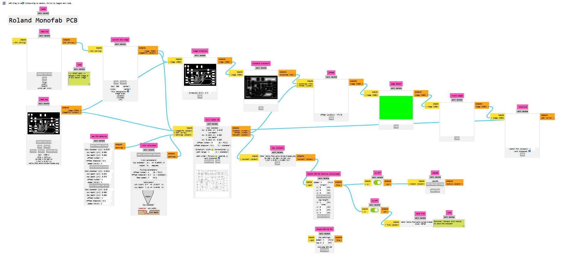
Generating toolpaths
To mill the board, I needed to generate toolpaths from the traces. I used MODS CE to generate this code.
I used the default settings in MODS excepts for the following minor changes.
Under "Roland SRM-20 Absolute coordinates":
origin: x,y,z  = 0,0,0 (mm)
home: x,y,z  = 0,0,5 (mm)
Setting the Z to 5 mm would keep the tool at 5 mm above the material, avoiding damage if the Z was moved to the home position.
Here are the steps I followed to generate toolpaths.
In MODS, load the "Roland Monofab PCB program":
Right click > programs > open program > Under "Roland : SRM-20 mill" > PCB CBA
To generate toolpaths, I did the following:
1. Under "read png", click "select png file" and pointed it to the interior traces file
    * be sure to do the outline file also

2. set PCB defaults > mill traces (1/64)
    * Choose "mill outline (1/32)" for the outline file

3. mill raster 2D > offset number = 0 (I wanted a clean board)
    * use only for the interior traces

4. Roland SRM-20 Absolute coordinates > set origin: x,y,z to 0,0,0
5. Roland SRM-20 Absolute coordinates > set home: x,y,z to 0,0,5
    * again, I set the Z home to 5mm as a cautionary measure

6. on/off > outputs out (to save the toolpath as an RML file)
7. mill raster 2D > calculate (generate toolpaths)
Start with milling the interior traces first.
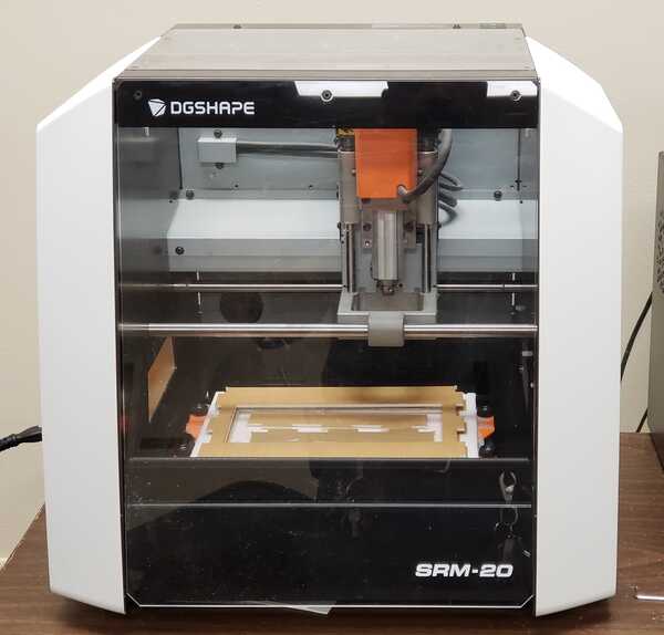
1) Mount the PCB to the spoil bed.
2) Install the 1/64 in mill in the collet.
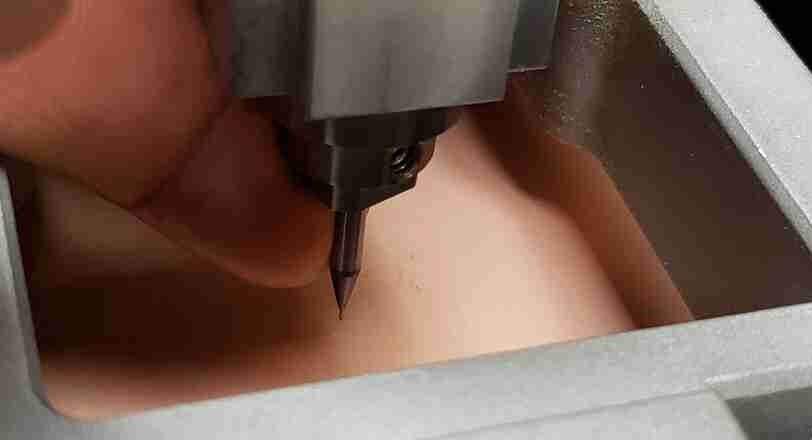
3) Start VPanel, make sure the tool is at a safe travel height, move gantry to an X,Y location relative to where the interior traces will be milled.
4) In VPanel, under "Set Origin Point", click "X/Y" button to register the X/Y origin point. For the Z, determine the best spot to register and move the gantry there. Once there, loosen the nut and slowly release the bit. Slowly lower it until it rests on the surface of the PCB and re-tighten the bit. Now register the Z level by cliking the "Z" button under "Set Origin Point". After registering the origin, raise the Z level to a travel safe height by clicking the "Z+" button before moving on. This will help prevent any accidental damage to the tool should someone start moving the gantry.
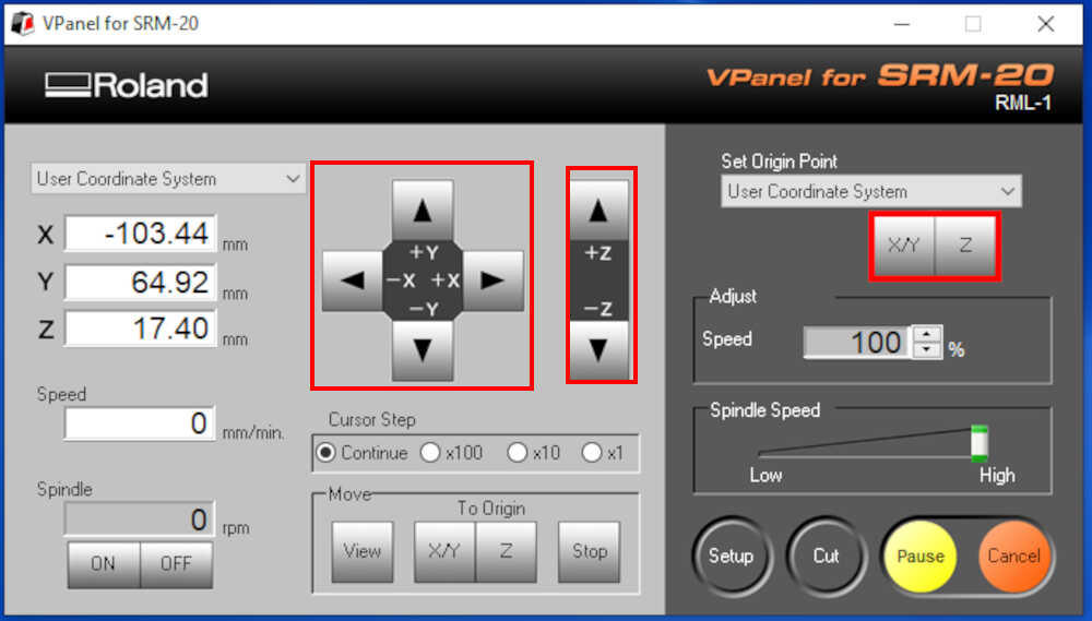
5) Now it's time to load the RML files which contain the toolpath g-code.
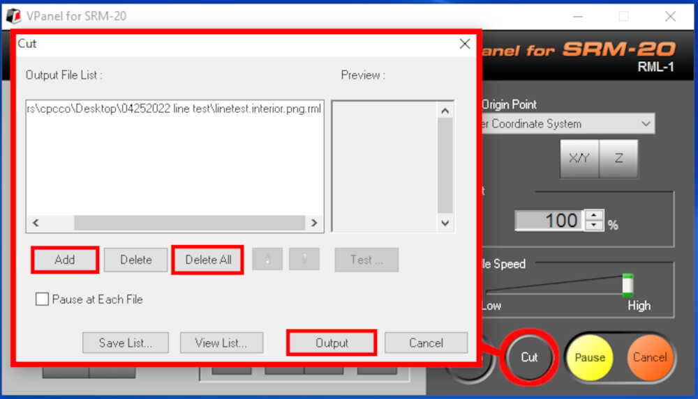
    1. Click [Cut]
    2. Click [Delete All] (if there is anything left in the "Output File List")
    3. Click [Add]
    4. Locate and click the interior traces RML file
    5. Click [Output] (this will start the milling)
6) Milling the outline is similar to milling the interior. Once the interior is done, I like to vacuum out the debris. Then do the following:
    1. Change the mill to 1/32.
    2. Make sure the mill is at a safe travel height. Move the gantry to where the Z origin will be registered.
        * Do not change the X,Y origin registration
    3. Safely lower the end mill to the surface of the PCB and Register the Z.
    4. Click [Cut] > [Delete All] > [Add] > load the outline RML file
    5. Click [Output] to start the milling
Problem:This image shows the results of my first attempt at milling the board.
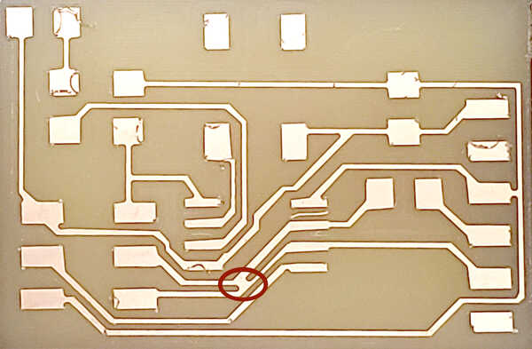
Ignoring the burrs for a moment, immediately I see a couple of problems.
- Two traces were too close for the tool to pass through (circled in red).
- All of the traces are very course and jagged.
What I learned:- A quick design rules check and checking the MODSCE outline would have alerted me to the problem before milling.
- It's also possible the jagged edges of the low resolution traces may have closed the gap so that the tool could not pass through.
What I changed:- I performed a design rules check, corrected the problem traces and modified other questionable areas.
- I exported to a higher resolution, 1500 dpi, but I believe 1000 dpi would have been sufficient.
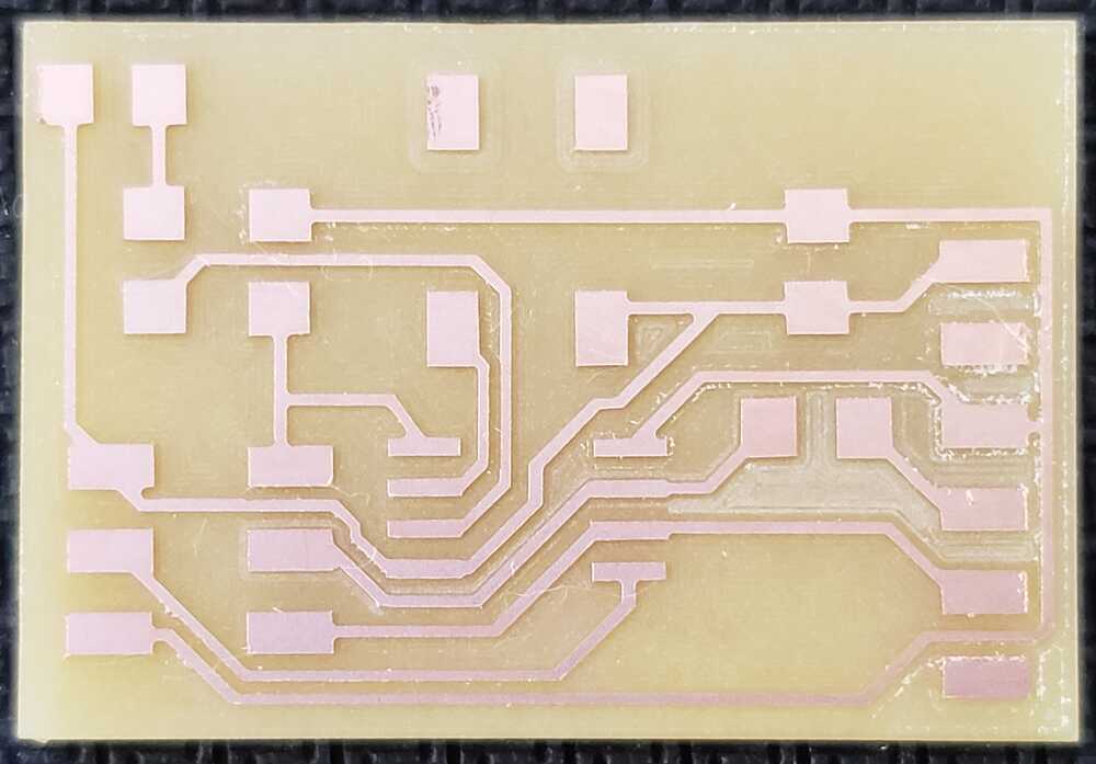
Here is the resulting board after making adjustments and milling the outline. The burrs have been removed. I have a cleaner board and smoother traces.
The board is stuffed and ready to be programmed. Additionally, I used a multimeter to verify continuity across traces and between components. I didn't get any images of myself soldering. I don't have a group to work with so as I got into the rhythm of soldering, I finished before realizing I didn't take any photos.
Load a program and test if your board works
As an initial test, I flashed the original code for the t45-echo board using my Atmel-ICE programmer. The addition of the LED and button shouldn't have any affect on this code and so this code should run properly, and it did.
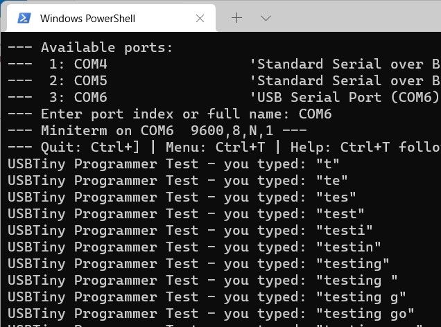
The second part of the initial test involves setting the PB4 pin on the T45 as an output and additionally set it to HIGH to put 5V on the LED to verify the LED is indeed functional.
Though I didn't do a preliminary test on the button itself, I was satisfied the board was ready and therefore any problems I might run into with coding wouldn't be reflective of the board itself but a problem with my code.
Demo
The video below is a combinations of 2 videos. It's not perfectly synced but it's close enough.

Downloads