Week08. Electronics Production
| Assignment | |
|---|---|
| group | characterize the design rules for your in-house PCB production process; extra credit: send a PCB out to a board house link |
| individual | make and test the development board that you designed to interact and communicate with an embedded microcontroller; extra credit: make it with another process |
Photo of the week
Lecture Notes
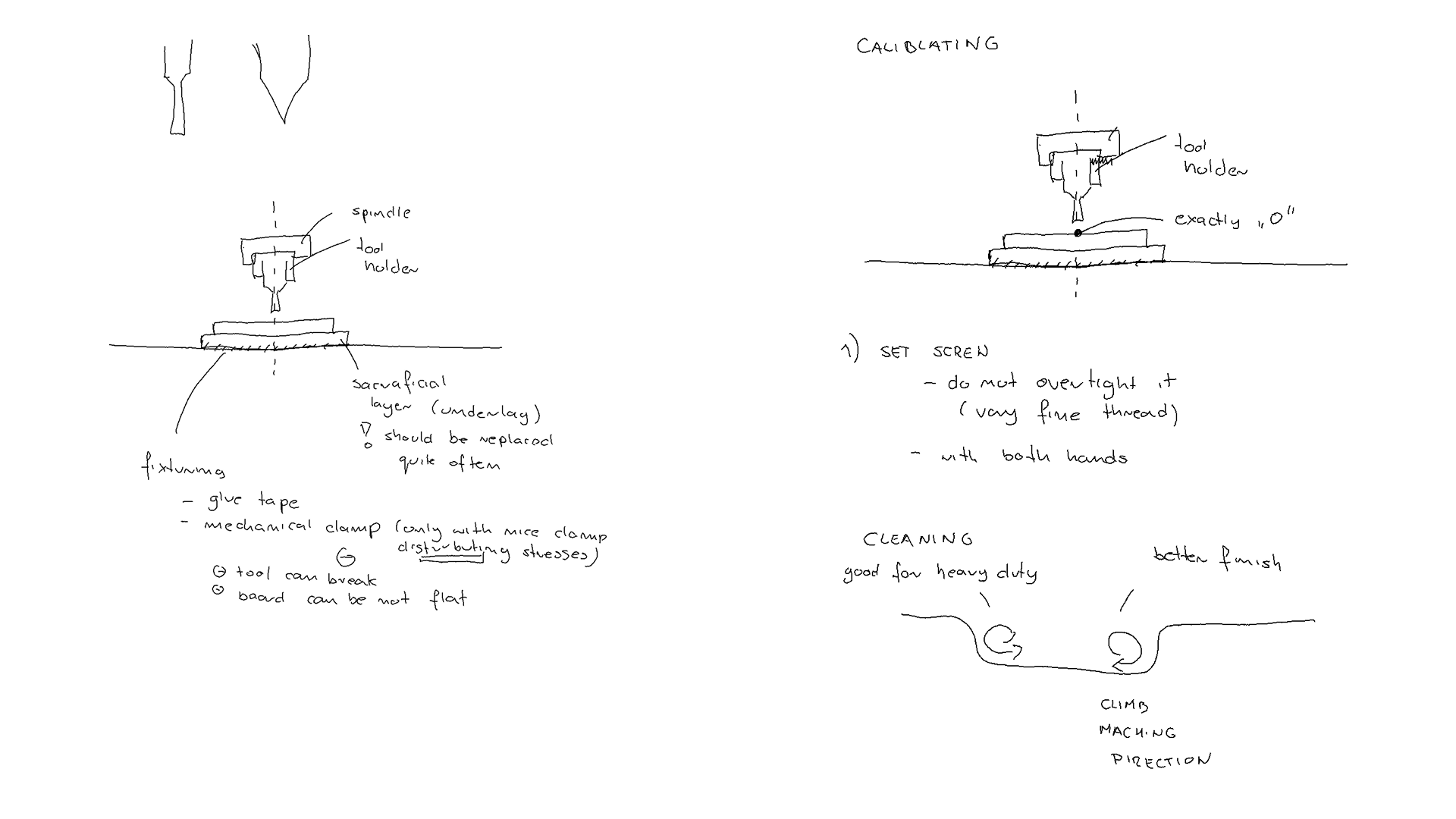
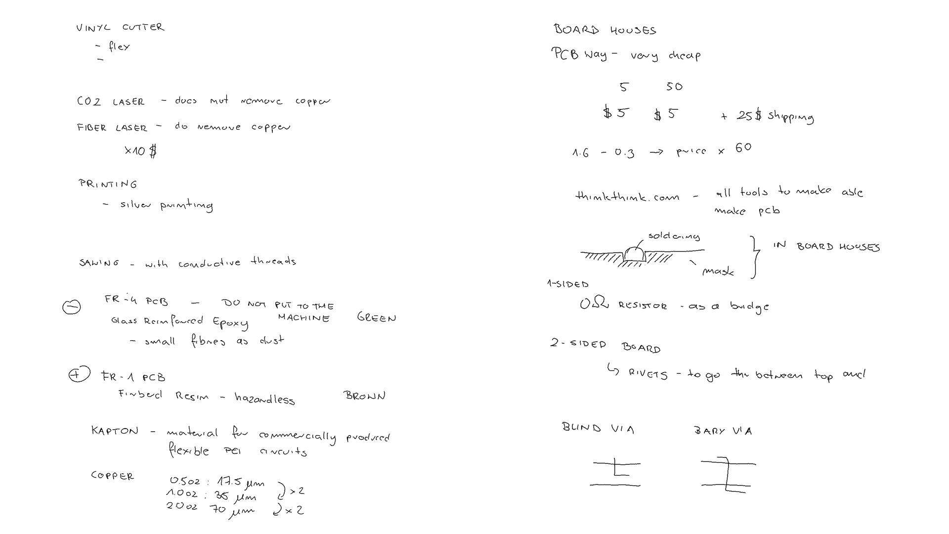
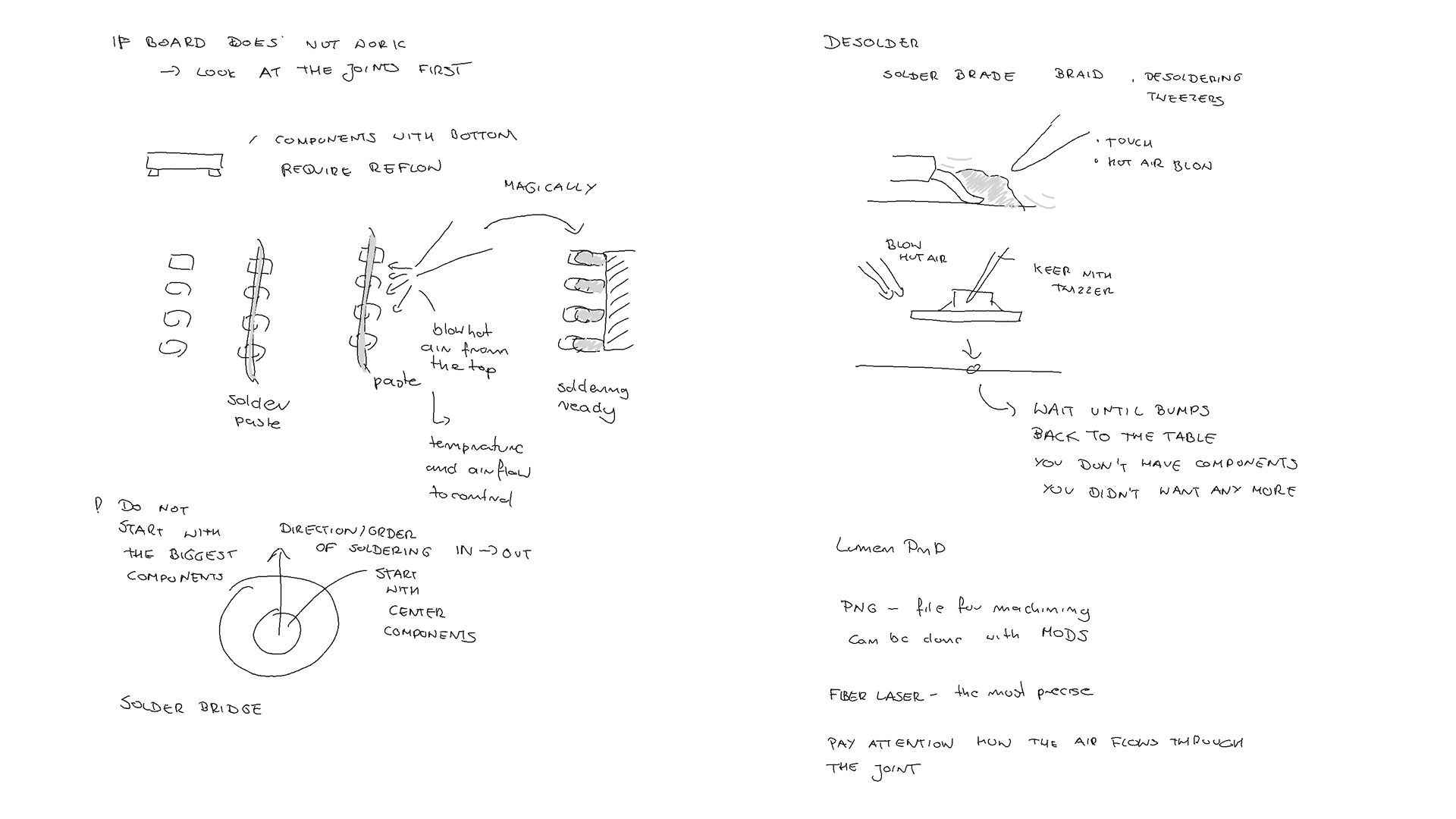
Take aways from the group Assignment
- min wire width and clearance 0.4mm
- a tip on calibrating the tool - screw it slightly > put it down > unscrew so that it hits the surface > screw it again
- workflow how to use mods to generate tool path on the local computer using linux on virtual machine
- 1/64in mill for traces & 1/32in mill for boarder
- tight the mill from both sides
Design
The design was based on the Adrian Torres Fab Xiao.
I had to improve the design of the PCB board from the week 6 Electronics Design due to the required wire width. 0.4mm wire width didn’t allow the wire to go between pin pads, therefore the board required rerouting. Moreover I also found one mistake in the schematic. The schematic of produced PCB board below.
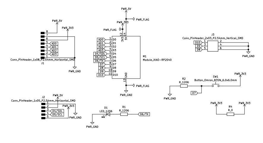 Fig. Final design - schematic.
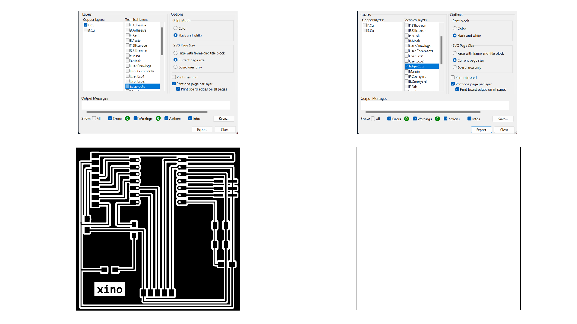 Fig. Final design -Exporting production graphics KiKad.
Production
The preparation of the tool path was prepared with MODS.
-
Read SVG: The svg file was imported to MODS.
-
Convert SVG image: important - set image DPI to 1000dpi.
-
Set PCB defaults: choose the right tool size and cut depth
-
Mill Raster 20: Calculate
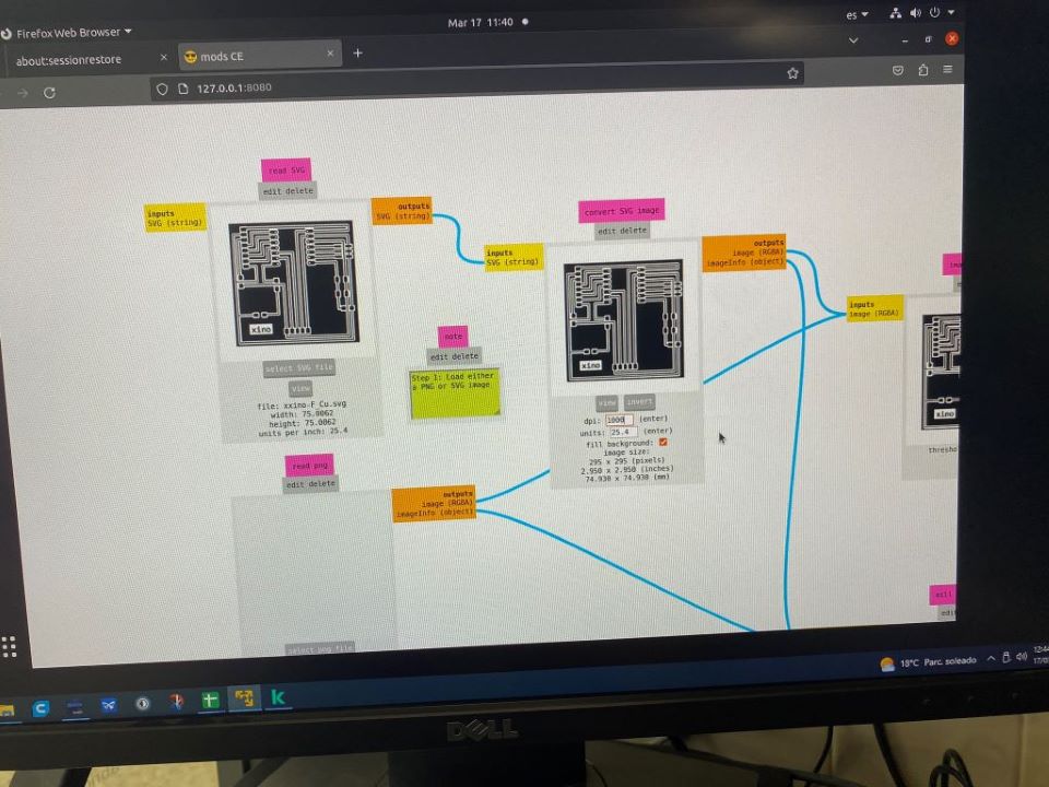
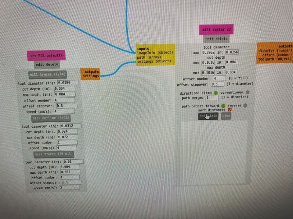
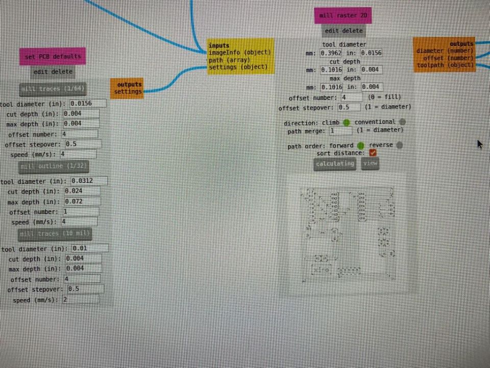
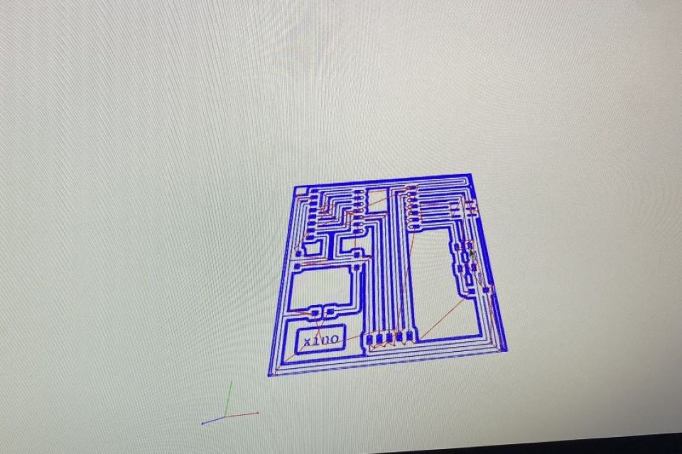
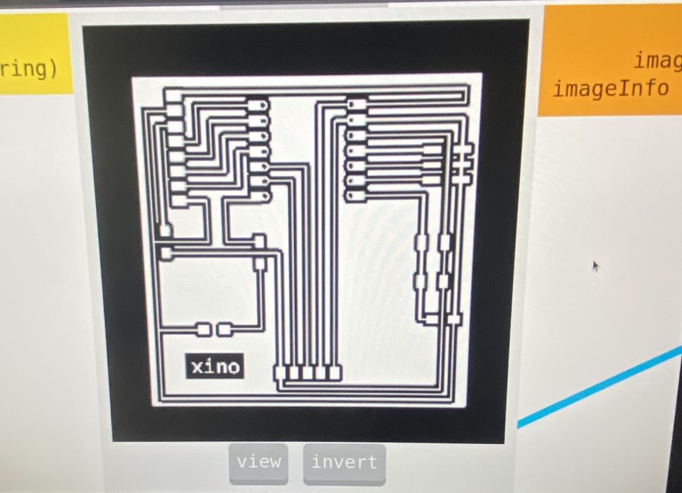
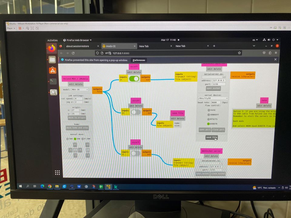
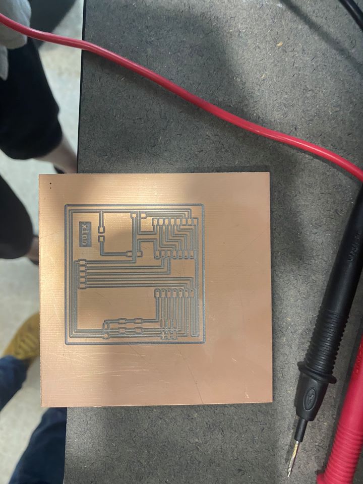 Fig. The first PCB produced - the V tool was wrongly calibrated (0 z-level) and it got too deep minimizing the wire width and breaking the continuity.
The tool for traces was recalibrated.
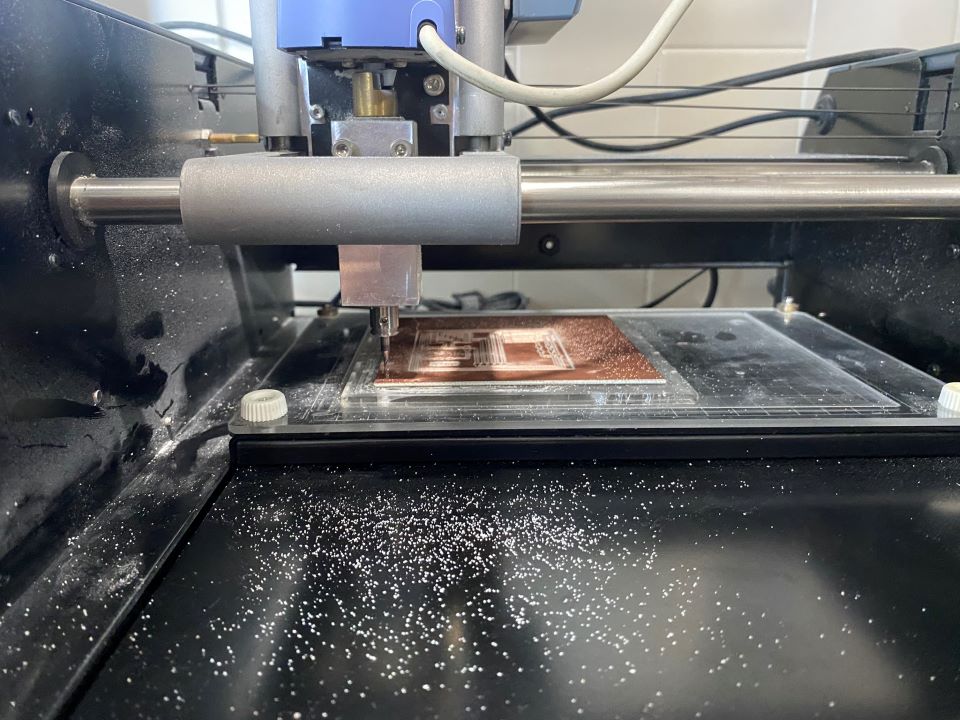 Fig. Proper Calibration.
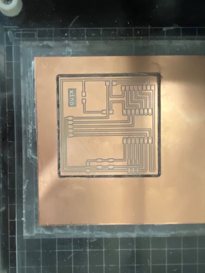 Fig. The final produced board.
Placing components & soldering.
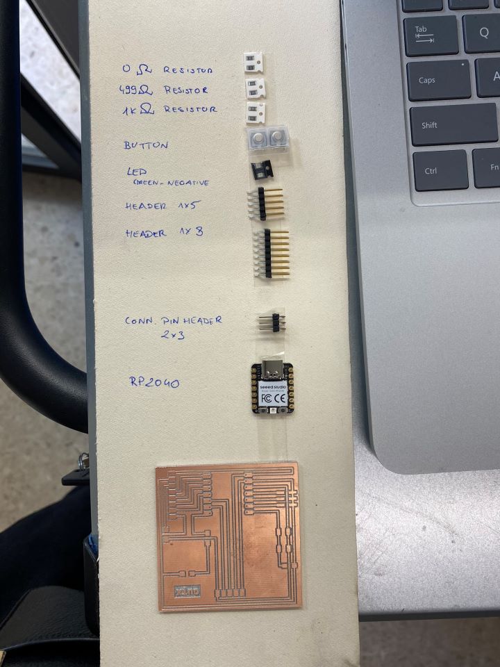 Fig. Board + components.
To solder:
-
make the sponge wet
-
turn-on solder (4.5/5)
-
clean the tool and soldered place with the solder cleaner
-
make the tip of solder wet (putting into the sponge)
-
keep the tip of the solder as close as possible to the component but on the ground (to not to move the component while soldering)
Diode: is one directional - green stripe to the GND
Button: one line of terminals on in-lined pads (just the terminals should be aligned with the traces - having some space on the pads for soldering)
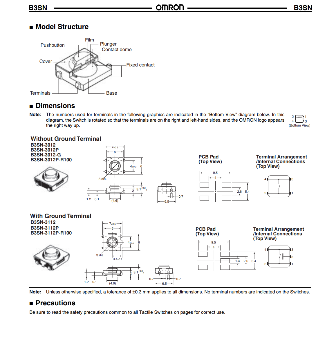 Fig. Switch Button.
Debuging
OHm - if OL (or a big number equal to the measurement when the multimeter ends are not connected with anything), - no continuity, if 0.0 - there is continuity.
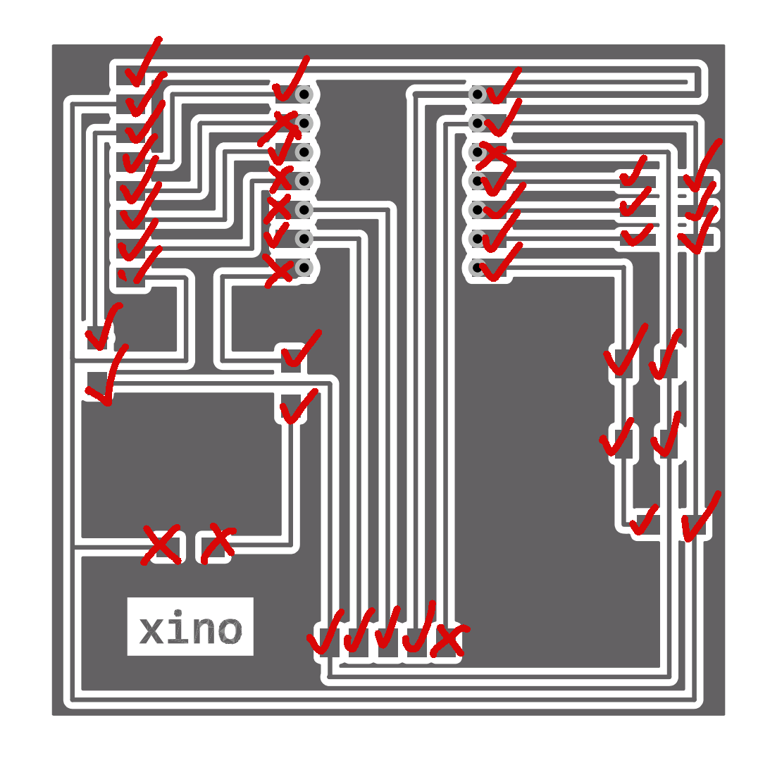 Fig. Points to repair the first soldering.
After improving soldering the measured resistance results:
-
Diode - OL ()
-
Resistor 0Ohm, - 0.0
-
Resistor 1000 Ohm - 0.999 kOhm
-
Resistor 499Ohm - 0.495 kOhm
Code MicroPython
The code in MicroPython to blink the diode. The diode is connected to the pin D6 (P0).
from machine import Pin, Timer

led = Pin(0, Pin.OUT) # default pin was 25
Counter = 0
Fun_Num = 0

def fun(tim):
    global Counter
    Counter = Counter + 1
    print(Counter)
    led.value(Counter%2)

tim = Timer(-1)
tim.init(period=1000, mode=Timer.PERIODIC, callback=fun)
Final Photo
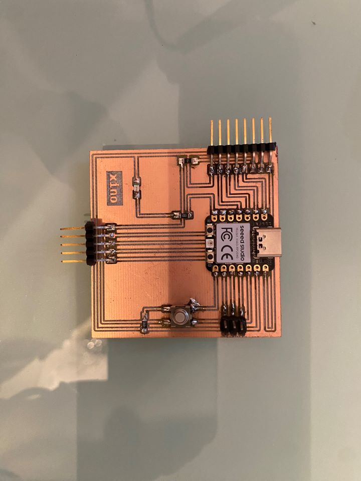 Fig. The produced board with the soldered components.
Final Video
Problems/Questions/Dilemas
- More clearance around traces (double the width?) - it makes it easier to solder, as the melt solder wire sticks to the copper parts.
- You can sort of feel, when the tool goes to deep - there are too many cut out dust.
- For connecting RP2040 to MicroPython, the bootload button needs to be pressed while connecting the board.
- Does diode has so much resistance that is doesnt show continuity?
Files
desing files: Xino - KiCAD
production files: Xino - SVG