
Summary
A fun week using several different skills. More soldering practice, a bit of puzzle solving when designing the PCB and a lot of magic/ luck when it comes to getting your components in the right orientation.
What I thought I knew before
My knowledge of electronics was limited by what i remembered from physics lessons at school all those years ago. It’s been some time ;).
Learning Outcomes
Theory and use of things i learnt from this assignment:
- Select and use software for circuit board design.
- Demonstrate workflows used in circuit board design.
Lessons to take away
Design PCB boards to match your expertise in soldering: Don’t position components on a board closer together than you can solder.
Risk Assessment
Milling & Soldering
See Week 4 - Electronics Production
Most used settings
Milling
See Week 4 - Electronics Production
PCB Design Rules
DESIGN RULES
| SETTING | DESCRIPTION |
|---|---|
| Min. Track Width | 0.39 mm |
| Min. Via Diameter | 0.4 mm |
| Min. Via Drill | 0.3 mm |
| Min. uVia Diameter | 0.2 mm |
| Min. uVia drill | 0.1 mm |
| Min. Hole to Hole | 0.25 mm |
NET CLASSES
| SETTING | DESCRIPTION |
|---|---|
| Clearance | 0.4 mm |
| Track Width | 0.39 mm |
| Via Size | 0.8 mm |
| Via drill | 0.4 mm |
| uVia Size | 0.3 mm |
| uVia drill | 0.1 mm |
| dPair Width | 0.39 mm |
| dPair Gap | 0.25 mm |
Limitations
Milling & Soldering
See Week 4 - Electronics Production
PCB Design
- Size of the board your milling machine can handle.
Operating instructions
Milling & Soldering
See Week 4 - Electronics Production
Work Flow
- Design your circuit.
- Make schematic diagram of components used in your circuit.
- Transfer schematic diagram to PCB editor and route tracks.
- Mill board.
- Solder board.
- Test board.
Individual Assignment
- Redraw one of the echo hello-world boards or something equivalent, add (at least) a button and LED (with current-limiting resistor) or equivalent input and output, check the design rules, make it, test it.
What I did
Design your circuit:
Using KiCad software tools, I opened a new project in the [Schematic View]. The assignment was to expand the Fablab “Hello-World” circuit with a button and an LED, so i started by referencing that diagram.

Make schematic diagram:
Using the [Place Symbol] button i added the components from the Fablab library to the diagram. It doesn’t matter really where the components are placed on the diagram, as the purpose of the schematic diagram is to make connections and relationships between the components. The [Assign foot prints] tool imported the dimensions and footprint of the components so you can see how much space they will take up on the board.
Adding [Global tags] to the various legs of the components allowed the software to know where and how the different components need to be attached. For human reference, i annotated the symbols using the [Annotate tool] and labelled the values of each component from the contextual menu > Properties > Values.
If needed, check with the component manufacturer’s website / data sheets on their function and how to map the different pins etc.
 Generating a Netlist using the [Generate Netlist] tool makes a list of which components are connected to which. This information will be used by the PCB editor program.
Transfer schematic diagram:
Open the PCB editor from the Tool menu. You should be presented with the schematic diagram on a PGB board, with all the components connected - resembling a ‘Rats nest’. If the Schematic diagram or Netlist hasn’t been transferred, use the tools to do so.
Now it is time to really ‘design’ the PCB by using the [Route Tracks] tool to draw lines between the components. Moving and rotating the components on the board is the first step. Trying to untangle the elastic lines of the rats nest that connect the components. These lines are only to assist and, its up to you to draw tracks around any that cross.
Tips:
- Rotate the components for easier routes.
- If the component is big enough, you maybe able to run a track underneath it and through its pads.
- Sometimes tracks may have to go around an obstacle and attach from ‘behind’.
To check if your design has met the design rules click on the ‘Ladybird’ button [Design Rules Check] to highlight any problems.
(If you’re having problems designing the routing you can ‘cheat’ by using the external “FreeRouting” software that will automatically find the best routing.)

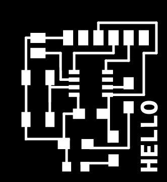
Once the design is finished, you’ll need to export different images from KiCad to send to the milling machine. Making sure that the diagrams have a defining border. This can be done by adding a closed path in the ‘Margin’ layer. Export as .SVG files to later import into Mods.
One for the traces, and one for the outline. Both need to be in black and white, with the white areas defining what will stay.
I imported the .SVG’s into Illustrator to tidy up any details, and add a ‘fake’ text trace on the board. Text is easier to manipulate in Illustrator (and i needed to outline the text to work). In the end Mods weren’t happy with my .SVG, so I exported to as a .PNG file instead.
Mill board.
To mill the board, see Week 4 - Electronics Production

Here the problems started, entirely with issues coming from exporting .SVG from KiCad and importing into Illustrator (see below). Eventually, i managed to create files that Mods was happy with, and delivered a good board.
Solder board.
To mill the board, see Week 4 - Electronics Production

Again, another exercise in trying to solder extremely small components. With enough magnification it was quite easy. I also used a little trick of sticking a bit of low-adhesive tape onto the component and securing it temporarily to the board whilst I solder the first end/pin of the component. This ‘third hand’ made it a lot easier to solder them in completely.
The biggest issue was to make sure that those components that needed to be positioned in a particular orientation. Referencing the schematic diagram, PCB design and data sheets for the particular components, I had a good idea how to identify the orientation and which way round to place them on the circuit. Only final testing will show if my educated guesses were right.
| COMPONENT | IDENTIFIER | ORIENTATION |
|---|---|---|
| IC (ATtiny412) | U1 | Yes (Dot over pin1 ) |
| UPDI | J1 | Yes Solder pins must sit flush on the board |
| FTDI | J2 | Yes (Solder pins must sit flush on the board) |
| Button (6x6mm) | SW1 | Yes |
| Phototransistor (NPN1206) | M1 | Yes |
| LED (1206) | D1 | Yes |
| Resistor 10kΩ | R1 | No |
| Resistor 5kΩ | R2 | No |
| Capacitor 1uF | C1 | No |
I also printed a little case to enclose the circuit and give it a bit more rigidity.
Test board.
Testing of the board consisted of two parts:
- Testing the electrical qualities of circuit.
- Testing the purpose of the circuit (can it be used as a programming circuit?).
Testing the electrical qualities of the circuit:
This consisted of using a Multimeter to measure: Continuity of the soldered joints either side of the component. A ‘beep’ shows that electricity can flow across the solder joints and through any path you choose.
I could also check the values of the components such as resistors and capacitors, using the Ohm, V or Capacitor settings. Since the LED is a ‘non-Ohmic’ component it wouldn’t show any values, however, get the probes on the correct ends and it will light up :).
With the help of another person, the button can be tested (pressed) to show that it will bridge the circuit with the probes placed either side of it.
The Phototransistor will have to wait to be tested by programming the circuit.
Testing the purpose of the circuit:
See Week 8.
What I should’ve done
I should’ve exported the files from KiCad as .PNG’s in the first place. I wanted to add the ‘HELLO’ text which was easier to do in Illustrator for me. Equally, i could’ve done that as a .PNG in Photoshop.
Mistakes & Issues

Surprisingly no issues with designing the board with KiCad. Sticking to the design rules and following my tips, it went well and quite quickly.
Illustrator .SVG files must be Saved as > More options > Responsive (unchecked) to be understood properly by Mods. Even after doing that Mods wasn’t happy making tools paths from it (red arrows everywhere on the track paths). So i exported a .PNG (at 300 dpi) from Illustrator instead.
Now, it turns out that there are more things you need to look out for when importing KiCad’s .SVG into Illustrator. Illustrator defines shapes using ‘strokes’ (lines) and ‘paths’ (closed polygons). A stroke is given a width, which, unfortunately for me, widens the dimensions of the pads on the circuit board. This caused the ATtiny412’s 8 very tiny leg pads to be joined together, without anyway of separating them.
To make sure the tracks didn’t share the same problem (they did seemed thinner than normal), I converted the tracks from lines into shapes themselves.
Outline files, i found out, need to include a closed black border. Mods doesn’t use the margins/boundary of the file as part of the milling path.
Group Assignment
 (image from Douwe)
- Use the test equipment in your lab to observe the operation of a microcontroller circuit board (in minimum, check operating voltage on the board with multimeter or voltmeter and use oscilloscope to check noise of operating voltage and interpret a data signal)
- Document your work (in a group or individually)
What we did

Multimeters
A Multimeter is just that. A gadget that can measure multiple qualities in an electrical circuit. Just not all at once. Most have some sort of a way to change which attribute your measuring, and some have a dial or something to change the sensitivity value of the read out.
By placing the probes in the correct places, they are able to measure:
- Voltage (Volts)
- Current (Amps)
- Resistors (Ohms)
- Continuity (See if current can pass in a circuit)
Ohm’s law states: For a given resistance, current is directly proportional to voltage.

Oscilloscope
 (image from Douwe)
An oscilloscope takes the voltmeter function of the multimeter a step further. Where the multimeter will output a simple value, an oscilloscope can visualise what the voltage is doing including over time.
The horizontal axis on the screen denotes the amount of time, and the vertical axis denotes the amount of voltage. Depending on wha the voltage is doing, the oscilloscope will plot a waveform of some sort. The most usual being a sine wave. Adjusting the knobs on the oscilloscope can refine the time scale, and voltage scale and where to plot the waveform on the screen.
Waveforms are ‘characteristic’ patterns each telling a different story of what the voltage is doing. These waves are measured by the number of times it completes a full ‘wave’ in one second, defined by the units ‘Hertz’ (Hz).
Some machines have the ability to do more than measure just one input at the same time, allowing mathematical functions to be performed on the output.
Operating the Oscilloscope Begin by resetting the machines knobs and buttons to their neutral positions. Set the [Volts/Div] to 1 and [Time/Div] to 1ms. Giving the waveform plotter a good starting point. Set the [Trigger] to Auto if the machine has the function, to try and stabilise any ‘wandering’ of the waveform graph drifting.
To test a circuit attach a probe to the [CH1] or [A]. Then attach the ground connector of the probe to the ground point in the circuit and touch the tip of the probe to the point of the circuit you want to test.
Adjust the [Volts/Div] and [Time/Div] knobs to clearly see the waveform, using the grid lines to measure the value.
What we measured: Testing an Arduino board, we measured the flashing LED function. This gave us a square wave, which after adjusting to get a clear picture of the waveform, we could measure the following attributes:
- The amount of voltage passing through the LED on each wave.
- How long the voltage was passing through the LED. And how long it ‘paused’ for.
- How many times a second it went through a cycle.
Mistakes & Issues
Always connect the GND lead of the probes (or connect to the GND of the circuit) before you use a second probe to do the measuring. This ensures the highest chance of safety for the board.
We were lucky to be shown how to pass too much voltage across an LED and short out it out, thereby ruining an Arduino board. It make a short, sharp crackling sound.
Always be careful of the angle you’re holding the probes of the oscilloscope at, making sure they don’t accidentally touch another part of the board at the same time.
CONCLUSION
‘Electrickery’ - Understanding electronics circuits continues to be part alchemy/magic for me. Choosing which components to use and what they need to be connected is abstract witchcraft - for the moment. I’m hoping more understanding will come through increased exposure and practice.