
Summary
From what i learn this week i will decide on what sensors to use in my final project.
What I thought I knew before
What i’ve managed to absorb from Weeks 4 + 6, ‘Electronics Production’ and ‘Embedded programming’.
Learning Outcomes
Theory and use of things i learnt from this assignment:
- Demonstrate workflows used in sensing something with input device(s) and MCU board.
Lessons to take away
-
No matter how meticulous in your preparations you are before milling, there is always an amount of ‘luck’ you need but you can’t control it.
-
Persevere!
Group Assignment

- Probe an input device(s)’s analog and digital signals.
- Document your work.
What we did
LOGIC ANALYZER Saleae Digital analyzer (8 digital channels, 24MHz)
This is a device that ‘sniffs’ the packets of digital data sent from / to the board for a specified amount of time. Using software this data can then be visualised in different ways to assess performance. This isn’t possible with a traditional oscilloscope without an expensive external adapter.
First thing I installed the software that goes with the analyzer, and opened it up.
Workflow:

-
Open a new ‘analyzer’ (RHS) Choose the type of chip/board you’re going to be testing.
-
Assign the pins/settings Depending on the chip/board and type of communication/protocol it uses, assign the channels of the analyzer to the pins.
-
Edit the simulation settings (LHS) Set the sample rate and duration of the test (‘sniff’).
-
Start simulation ‘START’
-
Examine the timeline for signals Change the ‘Decode Protocols’ settings (gear wheel RHS) to change the data format (e.g. Hex, ASCII etc).
Due to time schedules, it was a little difficult to make a group. I ended up getting together with Erwin one evening over a video call to go through the assignment. He was equipped with an Oscilloscope (and an old analyser which didn’t work) and i had a new Fablab analyser.

Originally i had briefly got together in a group after the teaching on Thursday. There we had tried to get a signal from one of our ‘Hello’ boards from week 6. We had used the ‘trial and error’ approach to plugging in different cable to the different channels on the analyser and the UPDI (Tx/Rx) pin.
Which thinking about it now, there was no communication element in the program that was on the ‘Hello’ board so why would there be any output form the UPDI pin. However, Paola did attach another wire/ crocodile clip to the analyser and tried touching various parts of the board in hope of a signal. And of course, touching the button with this ‘probe’ and pressing the button we got an input signal!
So after leaving that group early and working with Erwin, i was able to get a signal easily when the button was pressed. I dutifully explained to the more experience electronics expert how the software and the ‘magic’ black box worked (as his didn’t). And he nodded reassuringly.
Erwin then explained how he was getting an input signal on his oscilloscope from an Arduino creating a sine wave. Showing me the output and explaining what the graphs meant.

This was very helpful experience for me as i could ask all those little ‘Electronics noobie’ questions that fill in some gaps in my knowledge, and help to understand some of the bigger things. I left the video conference with a new sense of confidence in what i was doing in electronics (he also checked it looked like it should work and explained small things about my circuit).

With a probe I touched the LED and pressed the button. And this is part of ‘Hello’ in morse code as seen by the analyser.
Mistakes & Issues
Logic2 software starts from channel 0
A little confusing is that the number of channels in the software interface starts form channel 0, where as the pins on the analyser start labelling from 1.
ReadTimeout Error
Seeing this soon after you try and take a reading for the first time is a bit disheartening, but a quick google about the error and all it means is that the sample time has finished. Turning the ‘play button’ sign of the stat sample button into a ‘video stop button’ instead i think would be better feedback, but there’s probably a little more to the error; perhaps more input signals were detected outside of the sample time. Anyhow, something to ignore at this level.
Individual Assignment

- Measure something: add a sensor to a microcontroller board that you have designed and read it.
As always, after a global lecture’s worth of stuffing your head with a ton of new information and possibilities, my mind was shooting off at tangents about what i could make in this individual assignment.
I had 2 directions i could go in. One, use this a as trial run/practice of what i would need for my final project (very safe, not so exciting and easy), or two create something completely different (new, risky, useful and does something).
So obviously i first leaned in that direction. One word that stuck out for me in the lecture was ‘multi-touch’. This i thought would be cool as it opened up more possibilities for human-computer(/microcontroller) interaction. Simple electronics projects i’ve seen in the past (but never attempted) included small ‘pianos’ using a stylus for input and generating monophonic ‘sound’. With no idea how i would physically put my idea together, i thought making a polyphonic version of this small toy electronic piano would be a good implementation of multi-touch inputs. Even adding RGB LED’s to output a mix of colours depending on the chords you could play on the piano. Designing this board now would nicely setup an straight forward extension when it comes to the ‘Outputs’ week assignment - (other than the LEDs) namely speakers!
So then comes the research. What may seemed like a simple idea wasn’t. Words and phrases kept turning up like, ‘multiple timers’ and ‘midi patches’ for the sound generation and the reality of what i was capable of doing in this week dawned on me.
So back to an idea that would be within capabilities this week and help me with my final project. The simplest version of input for my final project would be to use a 6-axis accelerometer as the input (and based on the acceleration signals it gives, output eventually to RGB LED). Spiral development of my final project would include more sensors measuring multiple different factors to combine and output a more accurate and more sensitive result.
What I did
But where to start? The biggest hurdle for me is how to first get to a list of components that will do what i want? First thing i can do is make a list of design criteria that the board must meet and from that research and try to find the main components that are capable. Maybe i can get a few specification numbers from them that i can fit into an equation or two to move me onto finding what other accompanying components i will need.
Design criteria
This will closely match as possible the perceived design criteria for my final project.
- Small form factor. The final project is intended to fit on the wrist as a ‘wearable’ piece of technology.
- Powered by a button battery or ‘rechargable battery unit’. (3.3v-5v?)
- Include a 3/6 axis motion sensor.
With an eye on the future (assignments and spirals) a little thought should go into including the following list of criteria into the design.
- Space for more inputs in the future.
- Space for an ‘output’ (RGB LED or multiples of)
Initial decisions
The most important component is our course the input sensor, and then the next is the microcontroller / board on which it will control the signal it gives out. The Fablab inventory has a 3 axis accelerometer (ADXL343BCCZ-ND) and a simple search on the internet with this part number and ‘ATtiny’ (since that is the chip architecture we’ve used most and it’s ‘Tiny’) gave me a good idea of what to use. UPDATE I’ve been told that i’ll need to use ATtiny412 as my microprocessor.

Taking Neil’s 3 axis accelerometer circuit as an base example, there a few things I’ll need to redesign:
- UPDI headers, (instead of the ISP headers) with 2 pins (1 GND + 1 Tx/Rx async communication).
- Replace the ATtiny45 for an ATtiny412.
- ‘Delete’ the need for FTDI header pins by adding an extra 5v pin to the UPDI header pins (Suggested by Henk)

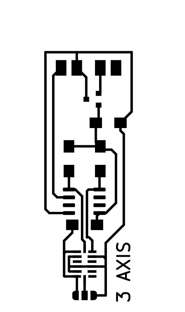
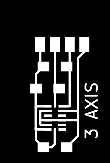
So I need to compare the 2 different micro-controllers and translate what the 45 does onto what the 412 does from their data-sheets. Check Neil’s coding to see what pins he assigned to the ATtiny45. Study the images of the traces, from KiCad and the finished board to try and work out what i should do.

BOM
To be ultra-safe and have as much support as possible, its probably best to try and source the components from the Fab Academy electronics inventory
| COMPONENT | DESCRIPTION | DATA SHEET | SPECIFICATIONS |
|---|---|---|---|
| ADXL343BCCZ-ND | 3 axis accelerometer | ADXL343-Datasheet.pdf | MAX V s / V DD = 3.9v |
| Extra Header pin | To connect to the UPDI+5v board. | ||
| ATtiny412 | Attiny212-412_datasheet.pdf | Polarity | |
| Voltage regulator | To drop the input voltage by 1.2 v for the sensor. | LM3480_datasheet.pdf | Polarity |
| Capacitor (1µ) | To stabilize power signal. | Non-polarity | |
| Resistor (10k) x2 | To control amount of current going to ATtiny412. | Non-polarity. | |
| CONN: UPDI 01x03 male | UPDI Tx/Rx communication, GND one component. And VCC, 5+V | ||
| Resistor (0 Ohm) | To use as a bridge for tracks to run underneath. |
KiCAD

- Set up project.
- Open ‘schematic layout editor’.

- Place ‘Symbols’.
- Attach ‘Global labels’.
- Place direct connections with ‘Wire’s if needed.
- Place ‘no connection’ where needed (to stop errors).
- Place ‘PWR FLAG’s to suppress power errors.
- Run ‘Electrical Rules Check’.
- Run ‘Assign PCB footprints to schematic symbols’.
- Run ‘PcbNew to layout printed circuit board’.

- Set design rules with ‘Board Setup’.
- Track ‘Routes’ and manipulate components rotation/position.
- Run ‘Perform design rules check’.
- Draw outline of board with ‘graphic polygon’ tool, on ‘Edges cut’ Layer.
- Export ‘.svg’, for the traces layer (‘F.Cu’) and interior layer (‘Edges cut’).
What i think the circuit does.
Power and GND comes in from two of the UPDI header pins, drops from 5v by approx. 1.2v in the voltage regulator to 3.3v. The power signal is then ‘smoothed’ by the capacitor. The current to the ATtiny412 is controlled by the resistors, and the sensors signal is synced and transmitted by connections to the SDA and SCL of the ATtiny412.
Board Production

Using the exported .SVG files from KiCad, I converted them into .PNG files in Illustrator (I remember something about Mods handling .PNG files more consistently). It was easier to get Mods to invert the ‘traces’ image than in Illustrator.
Imported into MODs and set the milling machine up to start the job. (for instructions see WEEK 4 and WEEK 6).
Obviously I had problems milling a board based on passed experiences; you can find them explained below.
Eventually after applying the correct design rules (not done at the right time), modifying footprints of components where needed, and exporting .PNG traces at 500dpi I was successful! (see above).
Side note: as I had modified the board to accept UPDI with a power connection, i will have to make a modified UPDI to work with my new board - 2 for 1 boards in this assignment. All that will be modified from the previous version were the communication female pins swapped to male pins, and a single one added to the +5v track of the USB. Jumper cables will be used between the male pins of the UPDI, and the male pins of the sensor’s board.
Soldering the board

The trickiest thing was always going to solder on the sensor as this was tinnier than the ATtiny!. Using the technique shown in Neil’s video i thinly tinned all the respective pads on both the board and the bottom of the sensor. I spent a lot of time and patience positioning the board. As you can’t see the where the pads of the sensor are from the top, its a game of getting it as straight and as centred as possible. Then came the hot air gun! I heated the area slowly around the sensor until I could see the solder melt on copper tracks. Pulling away a little to cool the solder slightly and hold the sensor in place. I was then confident to hold the sensor down with the pliers without it moving, and heat again to make sure the solder joined all the pads.
All the troubles i’ve had in the past with soldering vanished as i use my favourite flux to all the pads i was going to tin, then applied the components and with a light short touch with the soldering iron, everything was secure on the board. :).
I added a small piece of wire on the jumper to how Neil designed his board, which will be easy to remove or fix the other way around if I need to change polarity.
Overall, the soldering was the easiest and least ‘mistake’ prone part of this project!
Board Testing
A visual test with a loupe could only see how neat the soldering was. There looked to be no accidental shorts due to excessive solder use. But impossible to see under the sensor. Continuity testing of all the tracks and pins of the components that i could see showed that the soldering was successful. Next to the sensor the tiniest of pads was visible so i tried to see if they were connected properly with the probes. The SDa and SCl tracks and pins ran up the board underneath the ATtiny412, so I knew that no accidental connection had been made across from one side of the sensor to the other. Those meant to be connected from one side of the sensor to the other connected fine. UPDATE HOWEVER! Pin 3 on the sensor that shouldn’t be connected to anything, made a beep :( when one probe touched other tacks on the board. So it look all my steps to use the minimal amount of solder didn’t quite work (or the positioning isn’t quite straight) and a short is present under the sensor.
I even had a look at the board under the microscope camera to see any problems. Fascinating to see, but shows me nothing to concern me.

UPDATE
Reheating the sensor with a heat gun again to see if some of the very small amount of solder use can flow away. This worked as a continuity test ‘sounded’ that there was no connection between the sensors pins any more. :)
To check if the IDE could see the ATtiny412 on the board anyway I worked through the list of ports that Arduino IDE could see on my computer (Tools > Port) and tried to see what information it would give on the attached device with ‘Get Board Info’ (Tools > Get Board Info).
It showed that an ATtiny412 chip was present. :)
In preparation for a working board, When i can measure some data coming out of the sensor. I had downloaded and installed the Adafruit ADXL343 Accelerometer library to my Arduino IDE. This would be used in the programming once the board had successfully responded to me in Serial.
Due to the lack of serial (and any output feedback functionality), I borrowed some special probes from Henk to attach directly to the Rx and Tx pins of the ATtiny 412.
I uploaded a sketch to test if there was any Serial communication coming out. And there was!! :)

The values were very close together no matter what axis I shook the board in. From 1016-1018, which was at the high end of an analogue value. I could find nothing in the data sheet of the sensor to give me any clue as to what output to expect, so I assumed it would mean something when used in conjunction with the Adafruit library. ( I know now that its probably more to do with not using the right protocol and physical pins).
However, I could no replicate the results of the serial output again. The board had effectively stopped talking serial for some reason. I was advised to ‘move on’ to the current assignment as i had effectively got some reading out of the input as the assignment required. Just it wasn’t going progress much further.
So here is the code i had tried to modify from the example that came with the Adafruit library, if the board had worked.
I modified the ‘defined’ pins (MOSI, MISO, CS) to correspond with my ATTtiny412 communication (SDA/ SCL and CS). Once i have tried to fix the board I will start testing the code.

What I should’ve done
-
Made a ritualistic offering to the ‘Milling machine gods’.
-
Probably used a fresh new copper board that is more likely to be flat than using a half used one from the box of part used boards.
-
Added some serial output pins to debug.
Mistakes & Issues
Designing the circuit from scratch
My initial understanding of the assignment was to design the circuit from scratch. Probably a mixture of over thinking and panic, as this is a task beyond my current level of electronics understanding, although something i aspire to be able to do like Neil one day! So I should’ve started by ‘modifying’ an existing circuit to do what i wanted, which is still a difficult task.
Electrical Rules Check Errors

Had a few ‘Noobie’ errors with KiCad, I could easily solve these by adding a couple of ‘PWR flags’ assigning ‘VCC’ and ‘GND’ to them to the circuit knows where the power is coming from.
The other error just need me to add ‘no connect’ labels for the program to know not to expect any connections.
ATtiny45 / ATtiny412 swap
The biggest problem when swapping these IC chips over was that the position of th pins for the ‘SCL’ and ‘SDA’ were swapped over on the ATtiny412. After many hours of trying, and a failed attempt to install and auto router cheat with ‘Free routing’, I just couldn’t get all the ‘GND’ and ‘VDD’ connections of the components to route properly on the board. I needed to fins a trick where i could make one of the ‘VDD’ routes ‘jump’ over the ‘GND’ route.
KiCad not connecting tracks
Pins 4 and 10 on the sensor needed to be connected underneath the component. What ever i did i could not draw a track/wire joining them. Pin 10 wasn’t even visible on the schematic diagram.
I tentatively ‘modified’ the component’s ‘symbol’, where i found Pin 10 was selected as ‘non visible’. It was designated ‘NC’, not connected, so i made ‘visible’ and tried to add a global label ‘GND’ to it so the net list will allow the pin 4-10 connection. No luck. NO amount of changing the pin 10’s settings output/input/ bi-directional in the schematic helped. Out of desperation in the ‘Pcbnew’ view, and with the ‘wire’ tool selected i right clicked on the pin 10 pad and tried the ‘make track’ option. It worked!
Tracks not small enough
The tiny accelerometer needs small tracks. However, the footprint in the KiCad library requires a smaller mill bit than 0.39mm to work. I found this out after i had milled the traces already. Henk remembered a past student having the same problem and gave me a link to his site to see what he had done Illias Bartolini.
The solution he had found, was to modify the footprint given to the component in KiCad. He had kindly left his files so i could download and have a look. I examined the footprint in the footprint editor and was able to save it into a new library (one one inside my KiCad) - by right-clicking on the footprint name in the list on the left.

This inspired me to modify a footprint myself as a solution to (the following problem). Erwin was kind enough to check my circuit for me and queried Neil’s use of the sensor’s middle 7 pin, as this was designated the CS pin, but the line symbol above it in the data sheet meant that it had a polarity.

One that didn’t match the circuit of Neil. To give me the option of designing a board that i could easily switch that polarity Erwin suggested having a 3 part ‘solder jumper’. The sensor’s pin could attach to the middle pad, and a small blob of solder would bridge the connection with the side that worked (when i found out by trial and error ;)).

Above you can see the faint line of the ‘no go’ zone around the pad, with the size of the pad now being inside it. So no design rules broken!

Design Rules Rule!

Having managed to mill the tiny pads of the sensor, i noticed other tracks were merged :( . The cause was that i had (as a last step in designing the PCB) applied the design rules and tested my design against them at the last moment. The way the program interactively traces a path needs these rules set up at the beginning of the PCB design process to eleminate the possibility of such errors.

Image from Nadieh
Resolution of PNG files (500 dpi!)
With the tracks fixed in the PCB designer the .SVGs that i had exported were converted to .PNG in Adobe Illustrator as usual (Export > PNG). The usual high quality setting is 300dpi, which has always worked well. This time Mods couldn’t make tool paths from the .PNG for the new smaller pads either. I had noticed that Illias Bartolini had exported his files as 500dpi. So I went back into Illustrator and exported the PNGs at that higher resolution than it’s ‘Max quality’ preset of 300 dpi. Mods suddenly could see the gaps in the design now and make tool paths through them :).

Milling problems

I thought i had overcome the bad luck and all the possible problems you could have when milling a board were behind me. Unfortunately not, Mill bits, new in the morning, broke halfway through a job. Try as i might to put a new copper board on flat on the work bed, one corner was lower than the rest so failed to get milled completely. But my tiny tracks had finally been milled! Grrrrrr.
See week 4 for more milling problems.
UPDATE
Adding serial pins to the design I was wrong in the assumption that ‘communication’ tracks could be used between different protocols. Especially a Rx UPDI line could be used as a serial Rx line if assigned in the embedded programming.
SPI or I2C With my knowledge at the time (or lack of networking and communication protocols to be exact), I didn’t know that the sensor would need special pins for communicating. I thought serial output would be enough. It spoke in SPI or I2C, which I was advised to wait for that teaching week before i go down that rabbit-hole. Which meant, unbeknownst to me, I was going to fail that week whatever i tried.
UPDATE - A WORKING SENSOR - Week 14

Together with the ‘Controller’ board i made in week 13 for Networking and Communications, I attempted to make a new version of the sensor from which I could plug in to the I2C communication pins.
- Board design

This new design wouldn’t need an IC on the same board, so the bigger chip (ATtiny 1614) on the controller board would do the main part of the work and be able to hold the library needed for I2C communication.
I researched the use of this sensor by other students in the Fab Academy’s past, and found some that directly copied Neil’s board using a ATtiny45. Only a couple I found had tried to do this with the sensor on a board separate from the IC. Ilias Bartolini Esteban Martín Gimenez.
But nobody had ported the sensor to the new generation of ATtiny chips yet. So I would be the first to use it in combination with a ATtiny 1614 (ATtiny412 might not have enough memory to hold much more than the needed library - see issues Networking and Communications)
So i made a list of all the components that the different circuits had in common to make the basic design. Somethings I was unsure about, one circuit used 2 Mosfet transistors for some reason (not explained in the documentation), and an extra capacitor to smooth the power for the sensor (the control board already has one).
A check with Henk, and I would just have to make it to see if it worked.

An easy routing as it was so small and few components.
- Production
A quick mill, and solder and it was done! No not really. The modified footprint of the sensor had allowed the small tracks to be milled, but the challenge would always be soldering the sensor in the right place.
I thinly tinned the tracks on the board, and added a ‘bubble’ of solder onto the tiny pins of the sensor. Then i very patiently positioned the sensor over the tracks, getting it in the middle of all the tracks from every angle. Then with the hot air gun, I delicately held the sensor in position and heated the areas around the sensor. When the solder was hot enough i saw it flow along the tracks and now it was a gamble if all pins had connected to the tracks.
-
Testing
- Continuity testing
For the components i could test i did, but there was no way to test if the sensor had connected to the tracks properly, other than it not falling of the board.
- I2C scanning
The easiest test to do was to scan the I2C bus and see if an address would come back, acknowledging it could make communication with the sensor.
  #include <Adafruit_I2CDevice.h>

  Adafruit_I2CDevice i2c_dev = Adafruit_I2CDevice(0x10);

  void setup() {
    // Initialize serial port
    while (!Serial) {
      delay(10);
    }
    Serial.begin(9600);
  }

  void loop() {
    Serial.println("I2C address detection test");

    // Loop throuth all possible i2c addresses
    for (char i = 0; i < 127; i++) {
      // Send address
      Adafruit_I2CDevice i2c_dev = Adafruit_I2CDevice(i);

      // If response on address, print address
      if (i2c_dev.begin()) {
        Serial.print("Device found at 0x");
        Serial.println(i2c_dev.address(), HEX);
      }
    }
    // Wait 5 seconds, then rescan
    delay(5000);
  }

And the sensor is alive!!!!! It wants to speak. :)
- Serial output
So the next step was to see if it was saying anything now I knew it was able to communicate. I downloaded the arduino files from Ilias Abrtolini, and just throw it on the controller board to see what would happen. The code is mostly in C, which i didn’t quite understand. The Hex address in the code for the sensor was the same, i wasn’t sure about assigning the pin variables for PB3 and PB4 as these for the ATtiny45. Maybe it would give me a ‘helpful’ error if it didn’t work so i tried it anyway.
    #include <Wire.h>

    #define BUFFER_SIZE 25

    #define ADXL343_ADDRESS                 (0x53)    // I2C ADXL343 ALT Address
    #define ADXL343_REG_DATAX0              (0x32)    // X-axis data 0
    #define ADXL343_REG_DATAY0              (0x34)    // Y-axis data 0
    #define ADXL343_REG_DATAZ0              (0x36)    // Z-axis data 0

    int i = 0;
    int pb3, pb4;
    char buffer[10];

    uint8_t adxl343WriteRegister(uint8_t reg, uint8_t value) {
      Wire.beginTransmission(ADXL343_ADDRESS);
      Wire.write((uint8_t)reg);
      Wire.write((uint8_t)value);
      Wire.endTransmission();
    }

    uint8_t adxl343ReadRegister(uint8_t reg) {
      Wire.beginTransmission(ADXL343_ADDRESS);
      Wire.write((uint8_t)reg);
      Wire.endTransmission();
      Wire.requestFrom(ADXL343_ADDRESS, 1);
      return Wire.read();
    }

    int16_t adxl343ReadWord(uint8_t reg) {
      Wire.beginTransmission(ADXL343_ADDRESS);
      Wire.write((uint8_t)reg);
      Wire.endTransmission();
      Wire.requestFrom(ADXL343_ADDRESS, 2);
      return (uint16_t)(Wire.read() | (Wire.read() << 8));
    }

    void setup() {
      delay(2000);
      Serial.begin(9600);
      Serial.flush();
      Serial.print("hello_serial: starting\n");

      Wire.begin();

      uint8_t deviceId = adxl343ReadRegister(0x00);
      Serial.print(" deviceId: ");
      Serial.println(deviceId);

      adxl343WriteRegister(0x2D,0x08); // POWER_CTL register
      adxl343WriteRegister(0x31,0x08); // Full res register

      i = 0;
    }

    void loop() {
      //_delay_ms(500);
      delay(500);
      i++;

      int16_t x = adxl343ReadWord(ADXL343_REG_DATAX0);
      int16_t y = adxl343ReadWord(ADXL343_REG_DATAY0);
      int16_t z = adxl343ReadWord(ADXL343_REG_DATAZ0);

      Serial.print("x: ");
      Serial.print(x);
      Serial.print("\ty: ");
      Serial.print(y);
      Serial.print("\tz: ");
      Serial.println(z);
    }

Success!!!! Now to try and visualise this serial data Week 14.
CONCLUSION
Old problems and new knowledge. This week i’ve learnt a lot about basic electronics and and struggled again with the milling machine. I have successfully soldered the smallest thing in the Fab Lab electronics inventory (that’s a guess), and it even looks pretty! So a big win there this week.
Getting it to work is something i still need to work on!
FILES
| FILE | DESCRIPTION |
|---|---|
| Traces | The traces for milling. |
| Interior | The interior for milling. |
| ATtiny412 datasheet | ATtiny412 datasheet. |
| ADXL343 Accelerometer Datasheet | Accelerometer Datasheet. |
ATTEMPT 2
| FILE | DESCRIPTION |
|---|---|
| Traces | The traces for milling. |
| Interior | The interior for milling. |
| KiCad | The KiCad files. |