 Erwin Kooi
06 - Electronics design
This week focusses on electronic design. How can we translate a desired function into an electronic circuit? It will start with a general introduction into electronics and then move to the design and creation of a circuit board.
The assignments for this week are two-fold:
-
Group assignment:
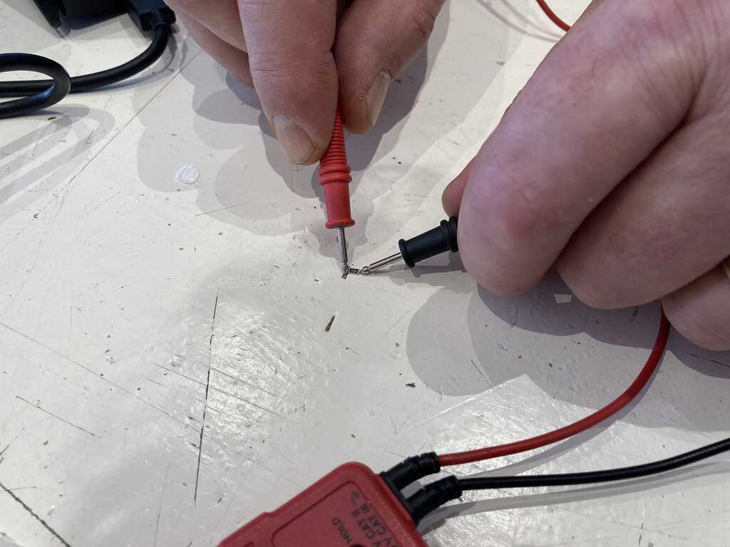
- Use the test equipment in your lab to observe the operation of a microcontroller circuit board (in minimum, check operating voltage on the board with multimeter or voltmeter and use oscilloscope to check noise of operating voltage and interpret a data signal)
- Document your work (in a group or individually)
-
Individual assignment:
- Redraw one of the echo hello-world boards or something equivalent, add (at least) a button and LED (with current-limiting resistor) or equivalent input and output, check the design rules, make it, test it.
- I have designed circuit boards before in EAGLE (with a purchased hobby license), but switched to KiCAD when they were bought by Autodesk. Most were double-sided boards with a mix of through-hole (PTH) and surface-mount (SMD) components. I have KiCAD installed and know my way around it.
- Creating a single-sided board with SMD components, no vias and no zero-ohm schematic wiresresistors, preparing it for milling and mill it as we did in week 4 is a good preparation for my home pcb creation process.
- Generating machine code from KiCAD that can be read by the GRBL controller on the CNC3018 mill (and bypassing mods) is something to investigate.
- Labels can have their uses, even in small KiCAD schematics.
- I am not the only one struggling with oscilloscope settings. (^-^)
- Mods is not as complicated as I first anticipated.
- The coffee at “Black gold” in Amsterdam is AWESOME!!! (thanks @Nicole)
- The cnc3018 mill will fit in my bike bag.
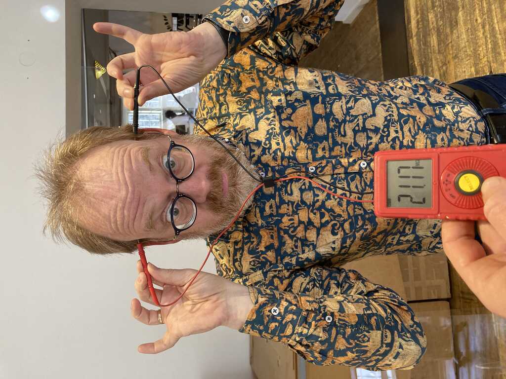
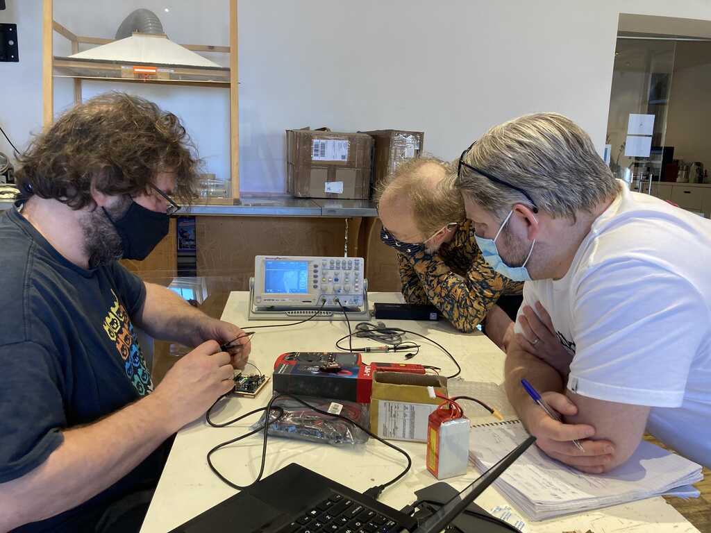
The group assignment revolves around working with test equipment in the lab. We will measure a number of components. A lot of time was spent on an introduction in electronics and I can imagine that this is very overwhelming if this is the first time you come in contact with it (even though it is literally all around us).
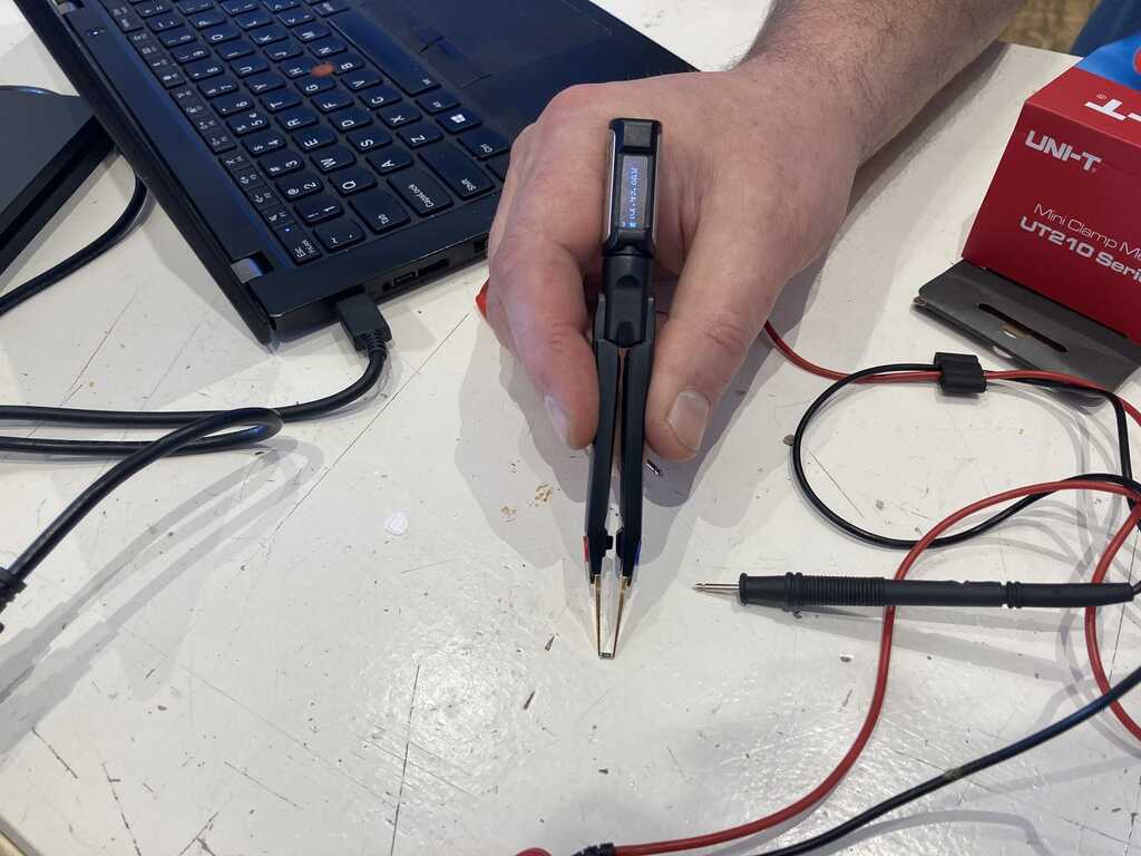
We measured components using the multimeter, but for smd components this is not the best tool. One moment of lapsing attention and the component flies across the room.
The node recently got some magic tweezers that will tell you the smd component type and value.
Yes, i ordered one…
If you define students as component, then you can measure them too…
The force is strong in this young padawan.
THen we got a very nice demonstration of magic smoke by Henk. When trying to show the PWM signal on a scope, there was that distinct snap and a puff of white smoke. The probe of the scope had shorted some traces…
For this week’s project, we are building a Hello World board. This board uses a microcontroller (an attiny412), an LED with current-limiting resistor, a button and a photo transistor. The attiny will be programmed using the UPDI interface we made in week 4.
The tool I like to use for designing PCBs is KiCAD. This program is developed by engineers at CERN in Switzerland and is used for component on the particle accelerators the have over there. The program is extremely versatile and flexible, but had a complicated user interface. But this has been greatly improved by the move from version 4 to version 5.
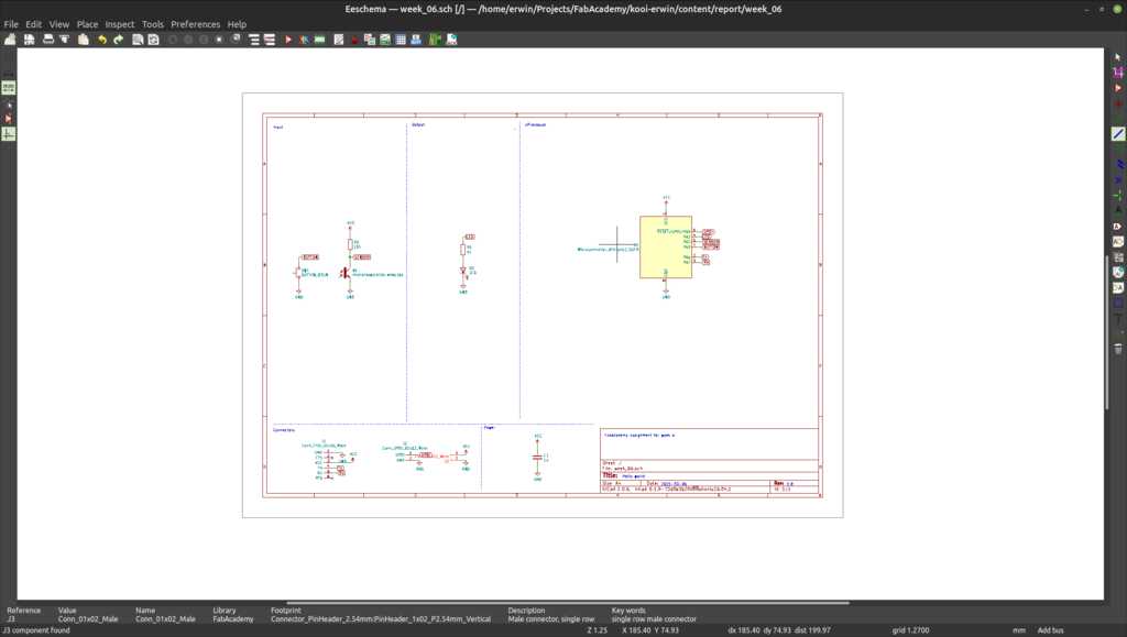
There are four distinct steps
- Design the schematic with the functional model of the comonents
- Design the circuit board with the footprints of those components
- Create the pcb and solder the components
- Test the board and fix mistakes
For the design of the schematic are basically two standards. Wire everything together
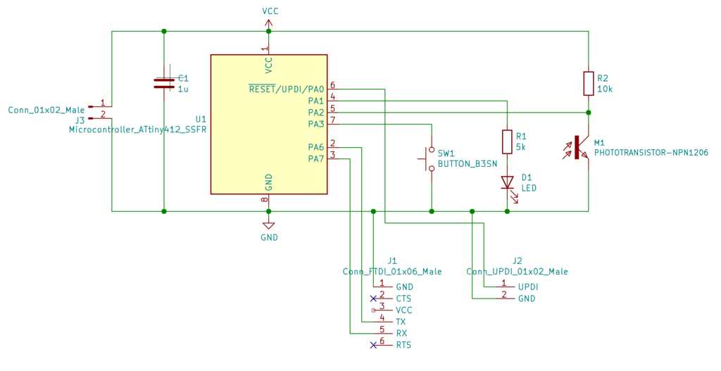
or label everything together
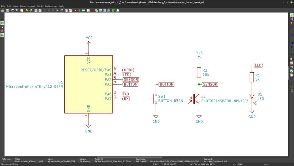
For small projects I like to use wires, but here I went the label route. This also allows groups of funcitons like inputs and outputs to be grouped together.
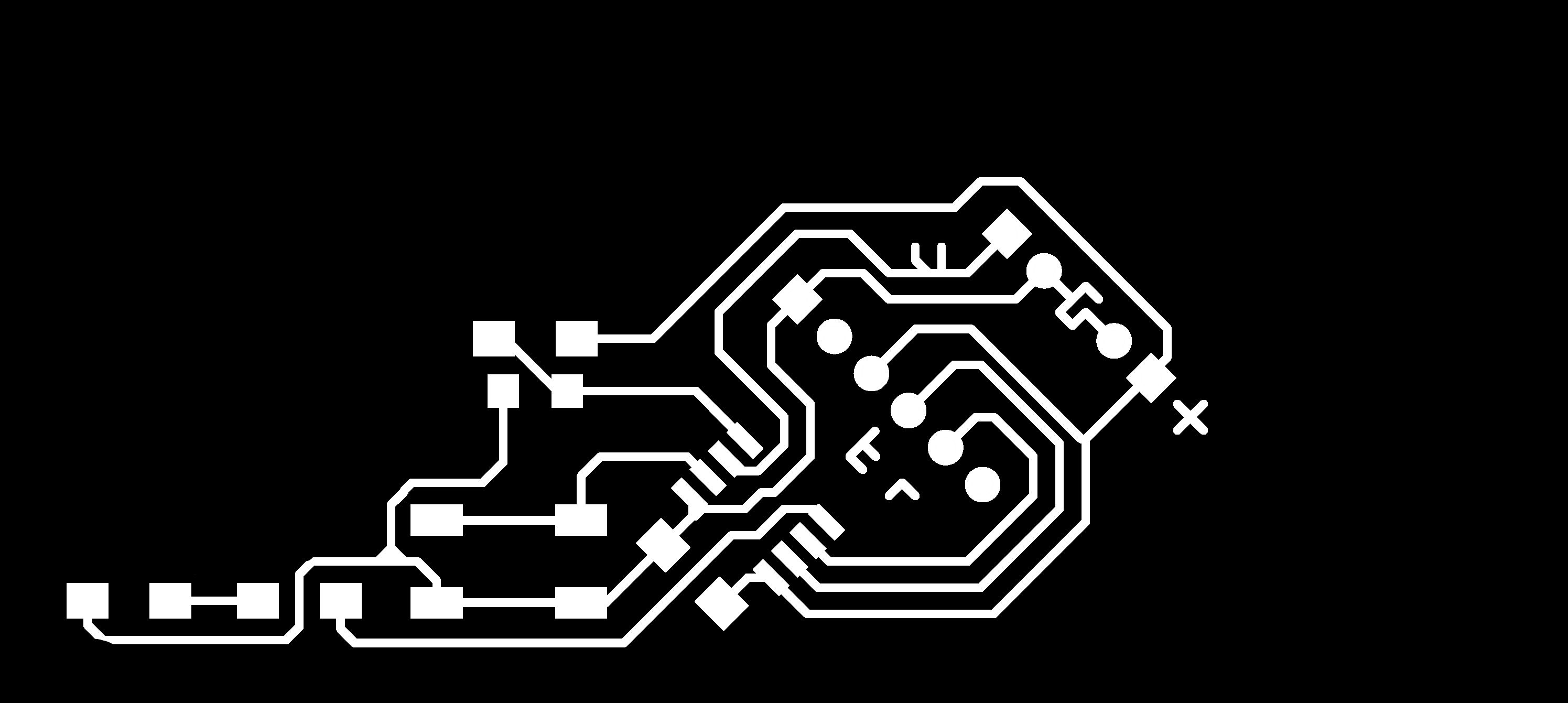
After the schematic has been created, the functional components have to be mapped to the footprint of physical components. Here you can tell KiCAD if you will be using through-hole or smd components, their size and their orientation.
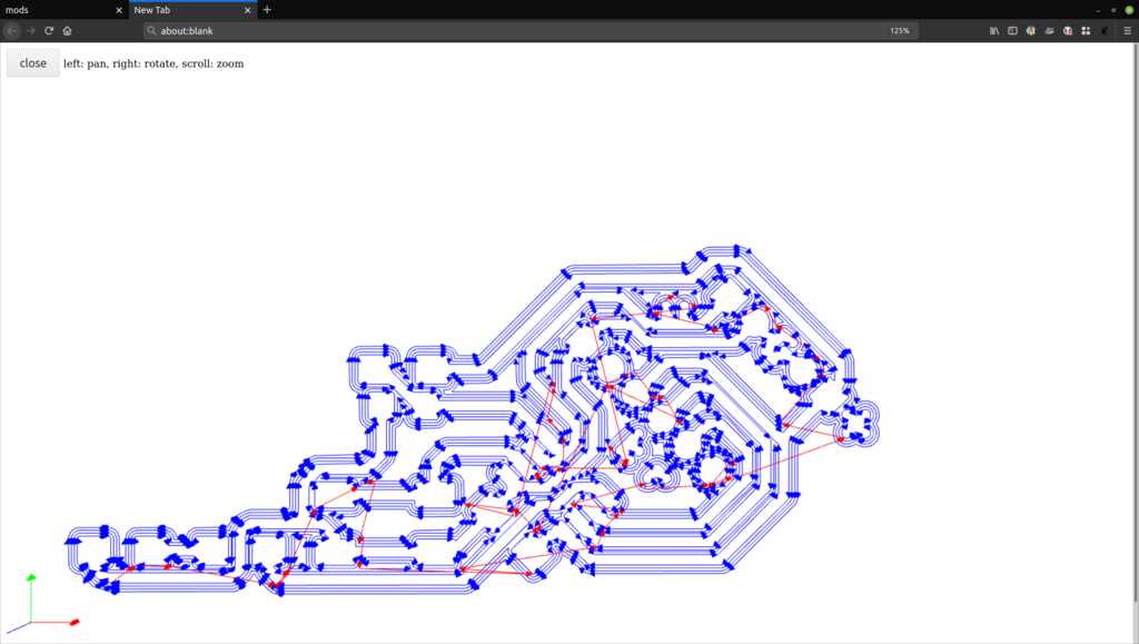
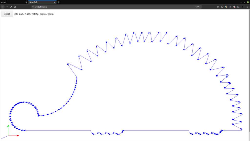
Then the zen-like activity starts of layouting the footprints and wire traces between them. This can be very relaxing, but quickly become frustrating when those last traces cannot be routed. :-) And at an unexpected moment, your alter-ego tries to influence the shape of the circuit board… The LED will be on the nose and the photo transistor on hie eye. The connectors for the FTDI, UPDI and power will be through-hole versions that will be soldered on the smd pads under an 45 degree angle. This will create the effect of quills.
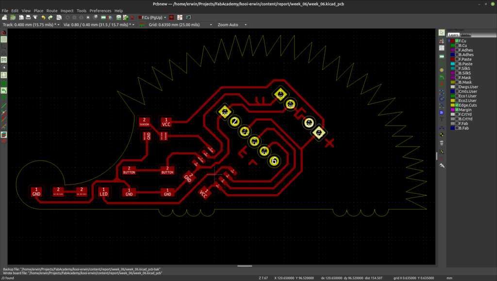
The fully routed board can now be produced. This is done on the pcb mill at the node.
The necessary files have been created with KiCAD and Inkscape.
Note that I removed the holes in the through-hole footprints of the connectors.
The traces along the outline are not necesary, but will create a nice effect after milling the board outline using the edge-cut.
And the final result:
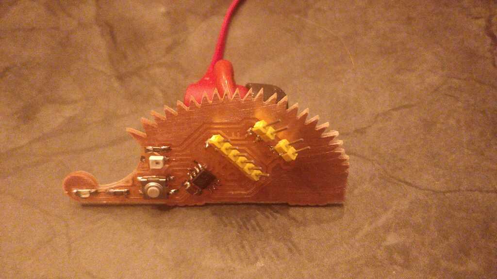
<tada.wav>
All traces have been tested for connectivity. In week 8, we will load firmware on the microcontroller.
The KiCAD project file can be found here.
The KiCAD schematic file can be found here.
The KiCAD pcb file can be found here.
The MODS file for the traces can be found here.
The MODS file for the traces without outline can be found here.
The MODS file for the outline can be found here.
The given current limiting resistor is 5k Ohm, but I think that is way too high.
The forward voltage of the LED is 1.8V.
- If the board is powered by 5V, this means the resistor has to drop 5-1.8=3.2 volt. 3.2V/5kOhm = .64 mA.
- If the board is powered by 3.3V, this means the resistor has to drop 3.3-1.8=1.5 volt. 1.5V/5kOhm = 0.3 mA.
LED’s typically require 20mA, so a resistor of 3.2V/0.02A = 160 Ohm (for VCC=5V) or 1.5V/0.02A = 75 Ohm (for VCC=3.3V) would sound more likely.
- The drawing of the schematic and circuit board went fine and the working with mods became much more fluent over time. I will also start using this for the workfloschematic wiress on my cnc3018 mill in my home-lab.
- I didn’t find the time to mill the pcb at the node. I will fix this by having my own mill in my personal fablab. Still waiting for some essential parts that are in the mail.
- I would check the size of the circuit board before milling. The hedgehog has now a somewhat flat bum…