7. Electronics design
This week I worked on designing, producing and programming a PCB.
I worked on a few simple designs of hello boards, starting from ATtiny44 and ATtiny45 microprocessors and adding the components needed for their functioning, with the addition of a switch and a LED diode.
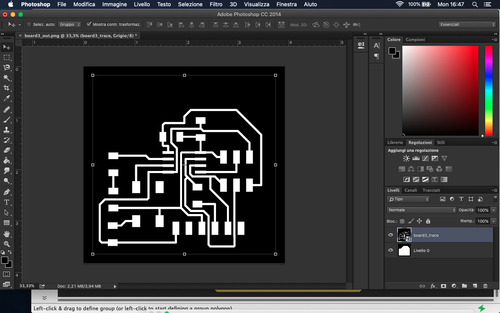
The software I used for the design is Autodesk EAGLE, I generated CAM files with FabModules
Design
It took me a while to understand how to design boards: not only it was problematic to understand what components I needed, but also to put them together. I also often found that my designs would not necessarily be ready to be milled straight away, but I had to make modifications so that they would be milled correctly.
Libraries
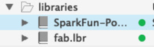
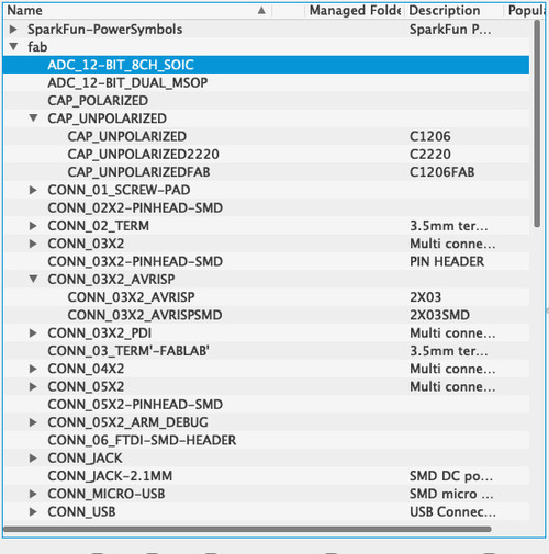
Before starting to design my boards I added the libraries of components I would need for my boards.
I download the Fab library from github for the components and the Sparkfun power symbols library to clean up my schematics page and to more easily understand what was happening on my board.
In Eagle a library is added by:
- moving the library file to the correct directory (Documents/EAGLE/Libraries)
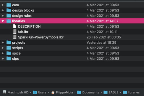
- activating the libraries by clicking on the gray dot in the drop menu
Schematics
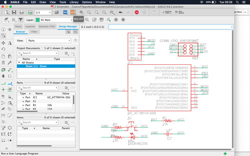
The first step in the PBC design was finding out what components I needed and compile a Bill of Materials.
I used the command Add to start navigating the libraries to find what component I needed. It’s important to select the components’ right package for the PCB.
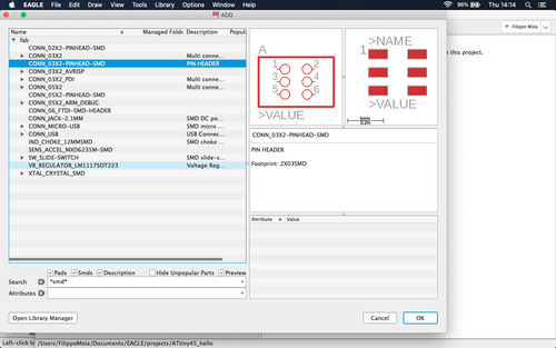
Left click to position the component in the schematic, right click to rotate them.
Once a component is placed, you can return to the libraries menu by pressing ESC.
I connected some of the components by placing them one next to the other, some others by using the command Net.

Once a Net is generate, you can connect them by giving two or more the same title with the command Name

For the components that need one you can add a value notation with the command Value

I tried to keep my schematics tidy and put the most closely connected components together in order to help me in the following steps.
I encountered some problems in the beginning when choosing pull down resistors, but I generally understood quite quickly how and what to connect.
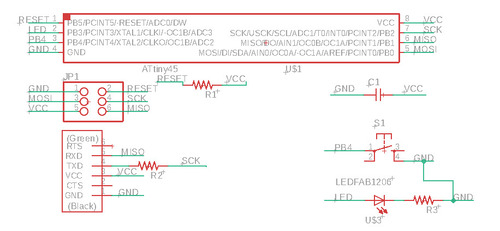
Here are some screenshots of my schematics design process.
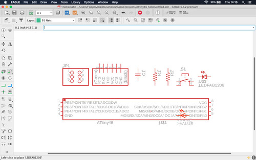
Before connections.
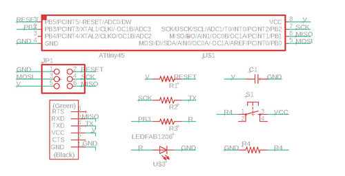
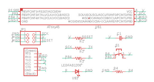
Various trial and errors. Sometimes I changed positions after having tried connections in the board viw and not managing to place and connect everything.
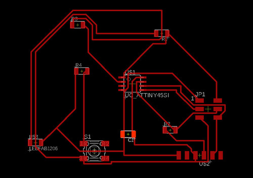
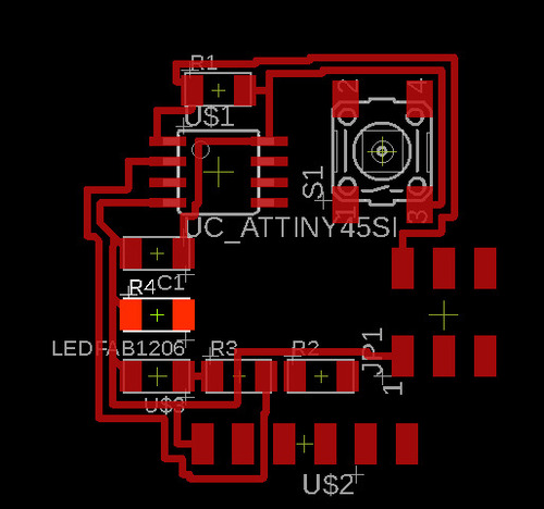
Final version.

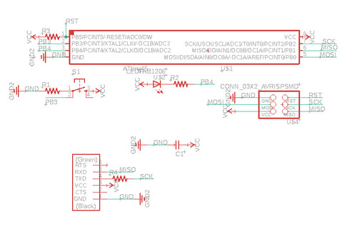
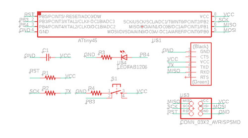
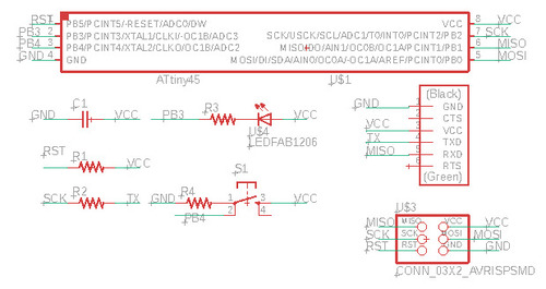
ATtiny45, Schematics
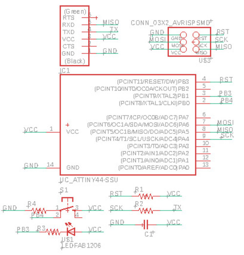
ATtiny44, Schematics
BOM
A Bill of Materials is generated by:
- clicking on Run ULP

- selecting Generate BOM
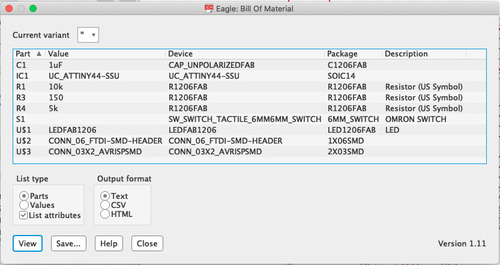
- choosing the preferred options and saving
ATtiny45, BOM
ATtiny44, BOM
Generate\Switch to board

In order to pass onto the final step of the design you have to click on the Generate\Switch to board.
This button will generate the components chosen in the schematics area and place them in the board view, and can be used to switch back and forth between the two modes for further modifications.
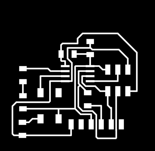
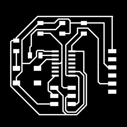
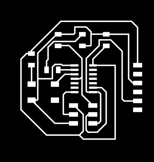
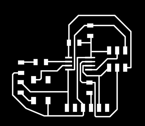
Board design
In this view you can move and rotate components by using the same commands as in the command area.
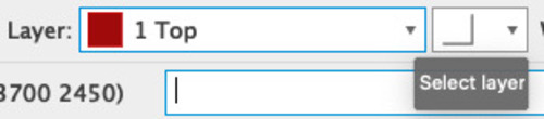
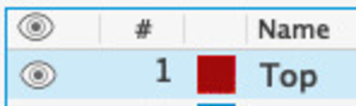
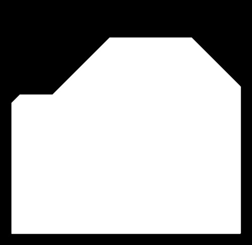
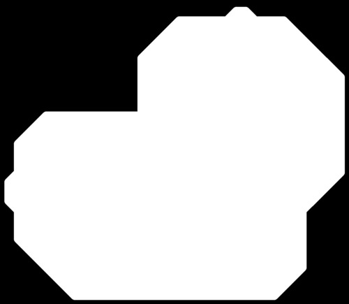
The layer on which to work can be selected with the drop menu, for my designs I only used the Top layer for components and traces and the Dimensions layer for the outline of my board.
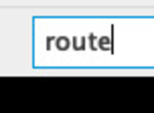
As opposed to the Net command in schematics, traces are placed by using the Route command.
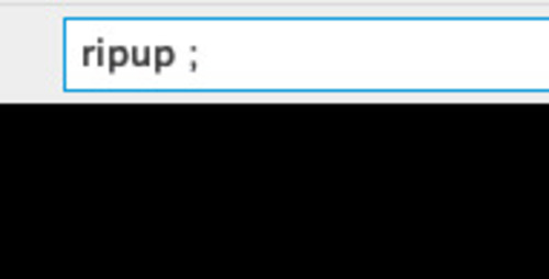
Traces are instead deleted by using the Ripup command, Ripup ; will instead delete all connections.
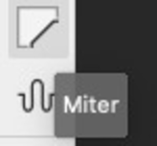
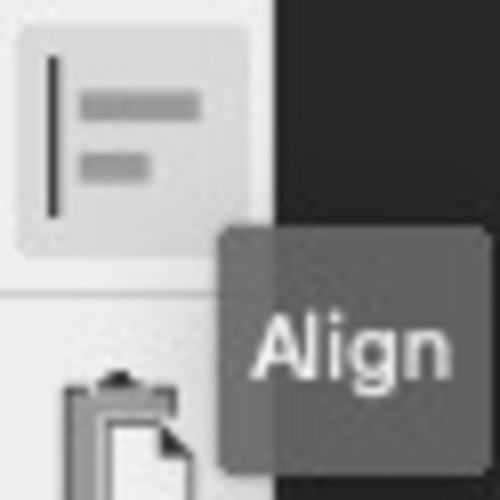
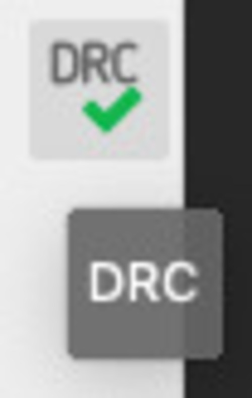
Other useful command are Align (to distribute the components on the grid), Miter (to smooth the angles) and DRC (to check that the design respects the design rules)
In the dimensions layer the outline is designed using the Wire command.

Components, routes and dimensions are cancelled using the Delete command.
The process of routing my boards was quite long as it took me a while to discover a workflow that was functional, as well as a way to prioritize routes and componets that would make this process easier.
It was a long trial-and-error process, but I found it extremely pleasant as there was an element of gamification as I started interpreting the routing as a puzzle.


I designed 6 boards in total and I think it took about 3\4 versions of each to finally get to a correct and complete routing, sometimes I tried the AutoRouting function in order to get an idea of how I could proceed, but I found it much more satisfying to solve the puzzle myself. I also found that my own routing were generally tidier and more visually pleasing than the ones generated by AutoRouting.
I only finalized two boards (the ones I considered best), in order not too waste too much material and components.
Grid
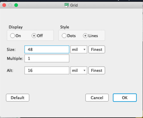
To make the board design process easier its helpful to carefully decide the grid options.
I decided to select the base movement as wide as 3 traces and the alternative movent as 1 trace, this helped me as I knew that in between componenent I would always have space for at least 1 trace.
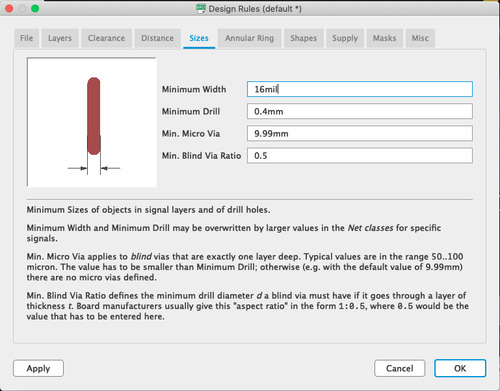
Design Rules
The two sections that I modified in Design Rules were Clearance and Dimensions.
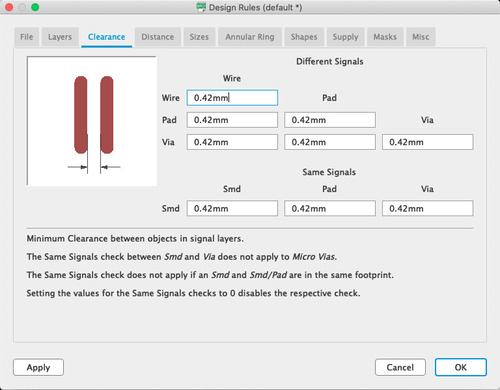
In Clearance I chose the distances in between components and traces, 0.42mm is a little wider than the mill end I would use in the CNC. In Dimensions I also chose measures related to my mill end.
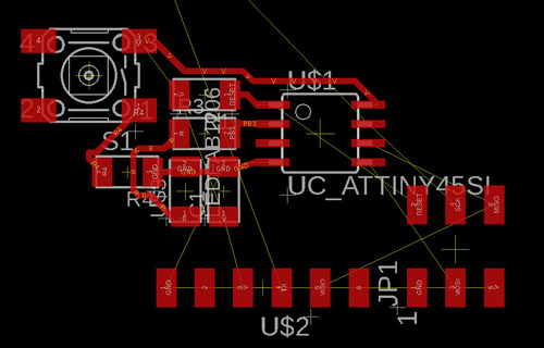
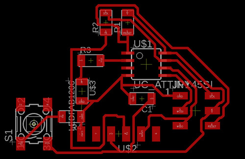
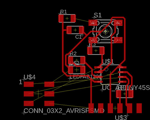
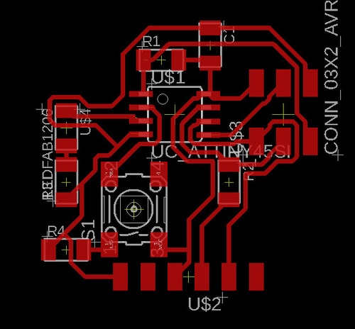
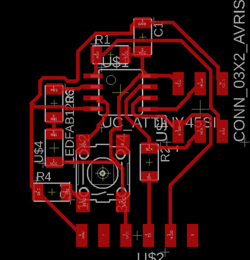
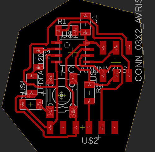
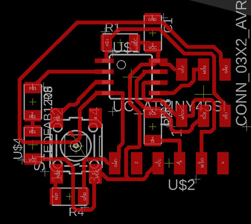
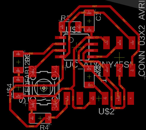
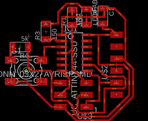
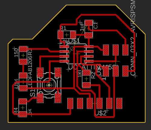
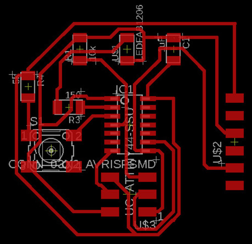
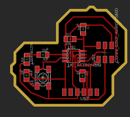
ATtiny45, Board
ATtiny44, Board
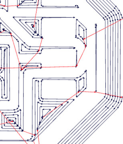
CAD to CAM
Once the board design is finalized, it’s time to generate a CAM file.
The way I operated was to generate a .png file, and feed that to FabModules.
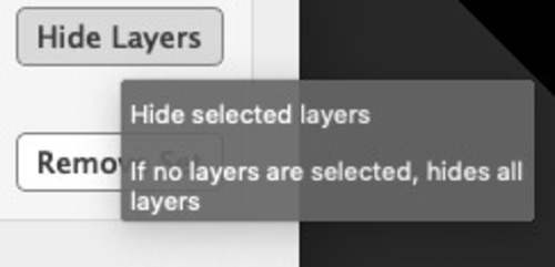
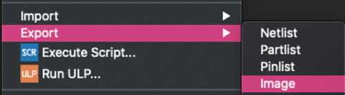
In order to export, you have to first hide all layers.
Than I selected which layer I wanted to export (Top, Dimensions).
For each layer you have to generate a Monochrome image at 1000dpi.
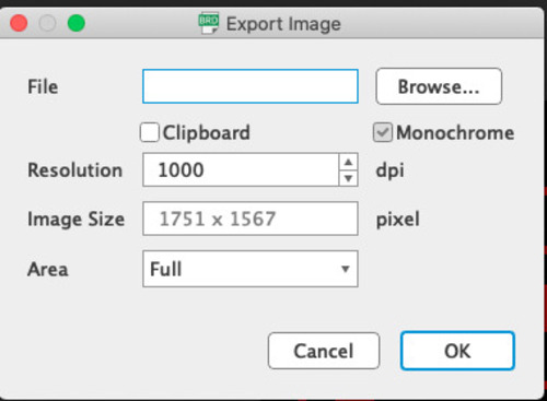
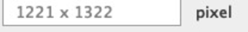
I noticed a small bug for that the images generated were 3 pixels bigger than how they were supposed to be exported, whith such high dpi, 3 pixels amount for a very small dimension distortion.

I then used Photoshop to fill the inside area of my outline layer, enlarge the black layer around the outline (so that it’s easier for FabModules to interpret the design), and then to match the dimension of the Traces image with the Outline image, so to assure alignment when machining.
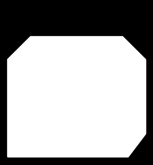
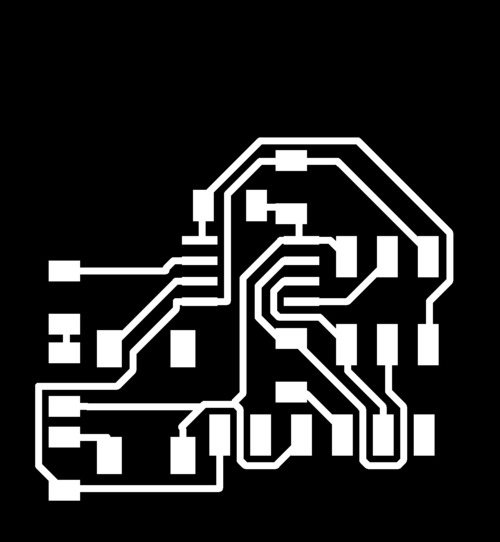
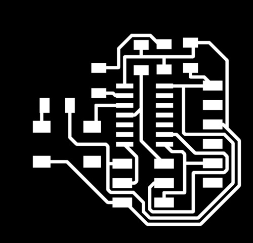
Here are the images exported via EAGLE and adapted via Photoshop of all 6 boards I ended up designing.


When generating CAM files i realized that even if I placed correct design rules, and my designs respected them (as checked with DRC command), sometimes FabModules would still not interpret them correctly, especially along diagonal lines.
Sometimes this meant I had to go back to my board to change the designs, sometimes I could trick FabModules by slightly reducing my tool size.
Example of a place were traces were fused together by FabModules.
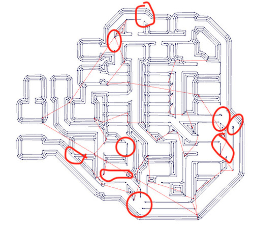
Every mistake in one of my boards.
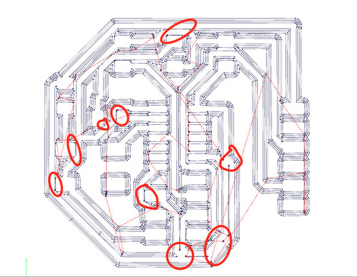
Every mistake in another one of my boards.
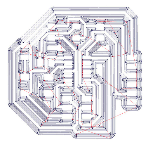
The CAM after fixing such mistakes.
ATtiny45 & ATtiny44 CAMs
- Board 1, Traces
- Board 1, Outline
- Board 3, Traces
- Board 3, Outline
- Board 5, Traces
- Board 5, Outline
- Board 6, Traces
- Board 6, Outline
Machining & Stuffing
For these two processes I followed the same workflow I described in my Week 5 page.
These included:
-
characterizing the machine
-
milling the boards
-
cleaning, deburring and sanding the boards
-
stuffing and soldering
-
testing my board with the voltimeter

These are two of the failed machining:
-
the one on the left was already presenting mistakes in the CAM I didn’t notice on FabModules
-
the one on the right failed because the board got detached from the sacrificial layer during the outline milling process
These were two board that I failed at soldering:
-
the one on the left was far too messy and I broke the led, but did not manage to finish solder
-
the one on the right was actually machined with a slightly off Z axis, soldering it was wuite complicated as the microprocessor barely fit, I also broke one of the traces
Programming
I also tried to program both final boards using the programmer I produced during Week 5 and Arduino IDE.
I installed the ATTiny CORE library in order to use my programmer.
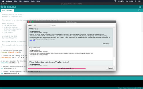
I used my FabOptimus ISP programmer that I prodeced a few weeks ago to program my boards.
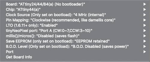
Only one of my two boards was actually programmed, as the second one is to be modified as the back of the FTDI connector touches a trace, generating a shortcircuit.
The board that is programmed has a slight problem at the moment as the internal clock seems to work erratically but I don’t yet know how to solve this.
Multimetre
Whenever I have been producing PCBs during the last few months, I have been using a multimetre in order to double check my traces and my soldering.
I have been doing this at various moments of the production phase.
Continuity
THis is the function used for continuity: if the red and black probes are touching traces that are connected, the multimeter will beep.
If there were some messier \ less precise milling, or very nrrow traces, I double check they are all correct just after machining.
After I solder the first necessary components to simply upload an empty sketch (ISP connector, reset capacitor and microcontroller) I check continuity of these.
After everything is soldered, I double check connections. If I had caused short circuits with bad soldering, I can try to fix them, I get confirmation I fixed it if there isn’t continuity anymore.
In this case, I have a badly milled board: in the video I show how, trying to follow the VCC line, some of the traces are connected (when it beeps) some are broken (when it doesnt’t).
Resistance
I have also used to check resistors value. This happened in the case I wasn’t sure I remembered the notation correctly, or when a soldered resistor had its value erased.
This video shows the value of a resistor used in this capacitive sensor (10megaOhm).
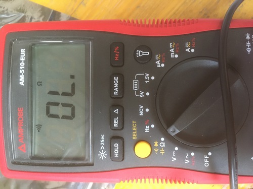
Current
Another way I used this tool was to check wether a board received the correct power supply, and that such current would go to the parts of the circuit where needed.
The current in this board is correctly 5 volts.
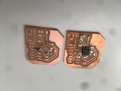
Pictures

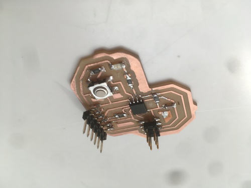
My ATtiny44 hello.world board (programmed, but internal clock in is malfunctioning).
My ATtiny45 hello.world board (FTDI,trace interaction to be fixed).
Files
-Schematics, ATtiny44 -Board, ATtiny44
-Schematics, ATtiny45 -Board, ATtiny45