Weekly Summary
This week's Electronics Design was another new chapter for me. Working with EAGLE was less complicated than I feared, I am happy I put extra work in to make the breakout connectors - and to keep working on my GameBoy Cartridge form factor. It's getting clearer and clearer that I will have to use the GameBoy Cartridges somehow in my final project.. as a way to store settings? to play different configuration?
Blinking the Board
Group Assignment
Use the test equipment in your lab to observe the operation of a microcontroller circuit board.
The group assignment this week was planned to be a work session with the oscilloscope. Unfortunately this had to be cancelled on short notice. Hopefully we can catch-up with this soon. Nevertheless, here is the link to the Group Assignment.
Individual Assignments
The individual assignment are:
- redraw an echo hello-world board,
- add (at least) a button and LED (with current-limiting resistor)
- check the design rules, make it, and test it
- extra credit: simulate its operation
This is again a week of discovery for me, first time I am using Electronic Design Automation software. My Gonzo-attempts at designing PCBs from Week 4 were fun, looking back now it already feels a long, long time ago.
Assignment Work Plan & Timetable
- Thursday: Local Lab Lecture, EAGLE Tutorials
- Friday: Re-drawing Hello World Board
- Saturday, 10:00 - 18:00 Lab Session in Kamakura
- Saturday: 12:00 - 18:00 Lab Session in Kamakura
- Monday, Tuesday: Documenting
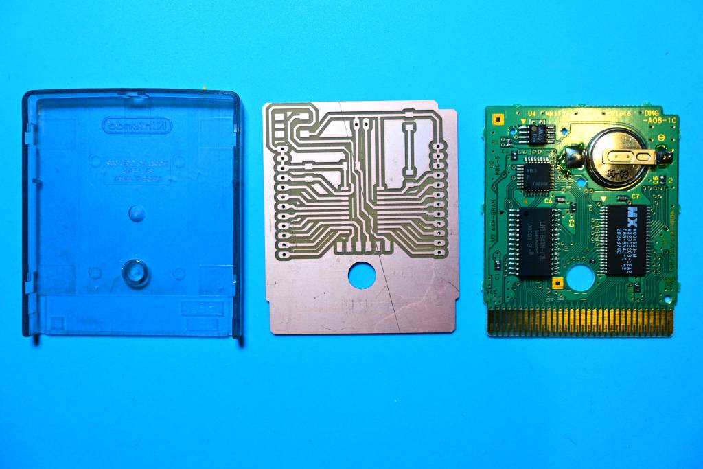
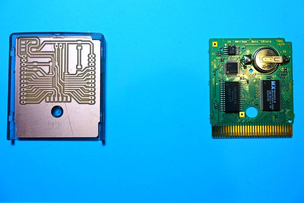
I will continue re-using existing packages, my plan for this week is to make the Hello World PCB in the shape of a Game Boy Cartridge PCB, with the ultimate goal of using the cartridge form factor - and the edge connector for communicating between the programmer and boards. (TODO: source edge connectors, without sacrificing GameBoys. If you know, where to find edge connectors for GB, please do let me know.)
Lecture Notes
Neil's other courses:
- MAS.862: The Physics of Information Technology: http://fab.cba.mit.edu/classes/MAS.862/
- MAS.865 2021: Rapid-Prototyping of Rapid-Prototyping Machines: How to Make Something that Makes (almost) Anything https://fab.cba.mit.edu/classes/865.21/
FabLab Inventory List https://docs.google.com/spreadsheets/u/0/d/1U-jcBWOJEjBT5A0N84IUubtcHKMEMtndQPLCkZCkVsU/pub?single=true&gid=0&output=html
AWG: American Wire Gauge Ancient Standard, wire needs to be thick enough for current it is carrying
Low Frequency: solid core High Frequency: stranded core
Surface Mount Parts
1206 size 12/1000 of an inch 6/1000 of an inch
The Art of Electronics Book. "Should be in every Lab!". Bible of Electronics, not only because of the content, but also because of the very thin pages.
More Lecture notes here.
About Electronic Design Automation Software
Autodesk EAGLE is a program for designing schematics and printed circuit boards for electronics - for Electronic Design Automation. It is currently (since 2016) owned by Autodesk and integrated in Fusion 360, but it has a longer history than that. The first version of EAGLE came out in 1988, E.A.G.L.E. actually stands for Einfach Anzuwendender Grafischer Layout-Editor (or, to directly translate it to English: Easy Applicablle Graphical Layout Editor).
EAGLE is not longer a stand-alone produce, a subscription to Autodesk Fusion 360 is necessary to use it. This prompted (and prompts) a migration towards open-source software, the main proponent being KiCAD.
FabLab Kamakura has experience with EAGLE - and as this is again a learning week, I decided to follow the recommendation and use EAGLE. Rico is currently deep-diving into KiCAD, with the hope of teaching future iterations of the FabAcademy with KiCAD. I will also have a look into it, but first, let's get this week's assignment done!
Installing EAGLE Libraries
After the intro tutorial on Thursday, Tsuchiya-san, the first steps are to set up EAGLE and import the library with the parts we will be using:
-
Fab Library
-
Atmel Library
-
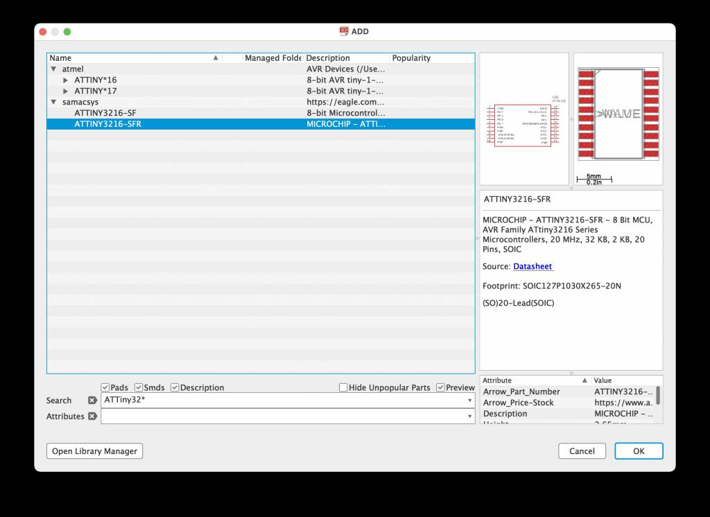
Samacsys EAGLE Library Plugin https://www.samacsys.com/eagle-library/ The Samacsys EAGLE Library Plugin lets you search for parts and footprints directly from within EAGLE. A quick walk-through of the installation procedure, more details at the official docs.
How to install on OSX
- Download the plugin
- In your EAGLE folder Documents directory, in my case
/Users/georg/Documents/EAGLE, find theulpsfolder:/Users/georg/Documents/EAGLE/ulps - Copy the
samacsys.svgfile to theulpsfolder, this will be the icon for the EAGLE workspace - Also copy
json.incandsamacsys.ulpto theulpsfolder - Open
~/scripts/eagle.scr - Add the path in
eagle.srcto both the BRD and SCH Menus:
'[/Users/georg/Documents/EAGLE/ulps/samacsys.svg] SamacSys : Run samacsys.ulp;'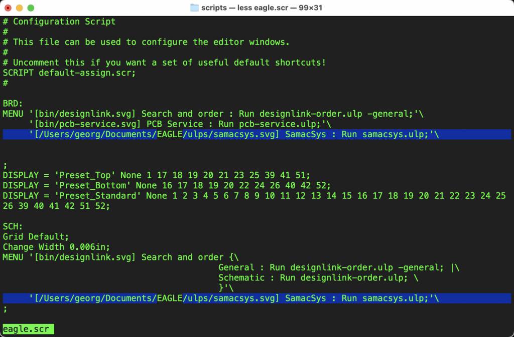
If everything works (and no mistakes in the paths!), the Button should appear:
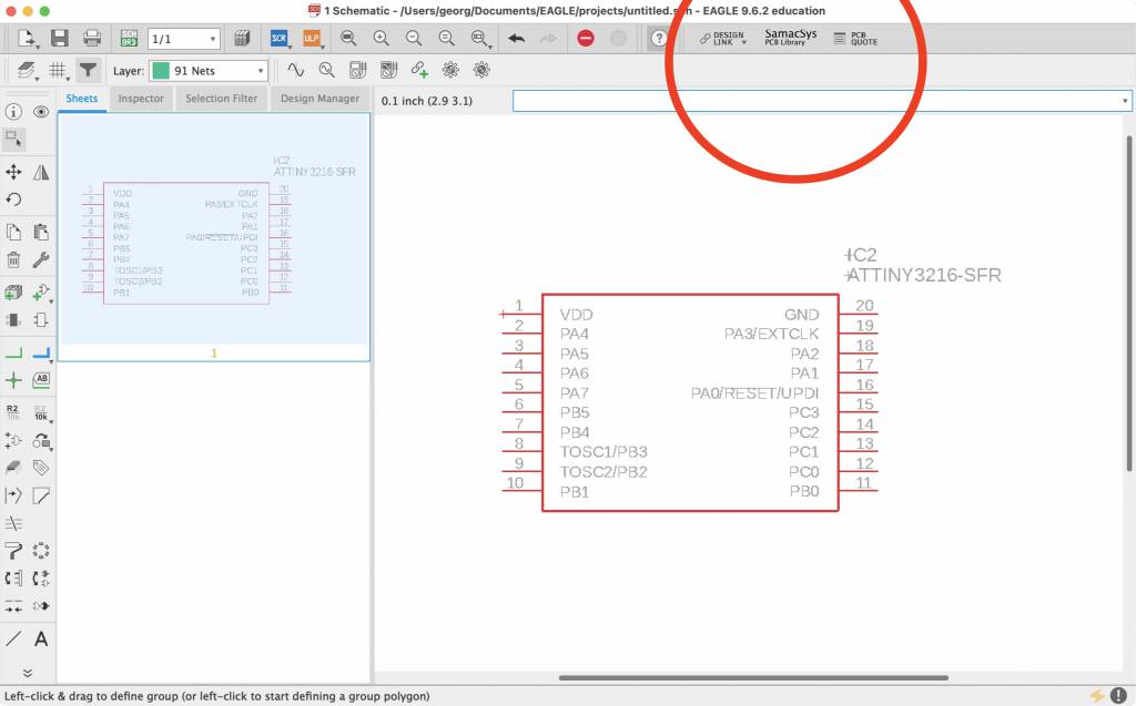
Clicking the Button brings up the Samacsys window, and after a quick login/register dance, the library becomes functional.
The Echo Board
The assignment of this week is to re-draw an Echo board, and add a button and a LED. The Echo board consists of an IC and connectors and when sent a Serial signal it will echo it back. That's why they are called Echo Board.
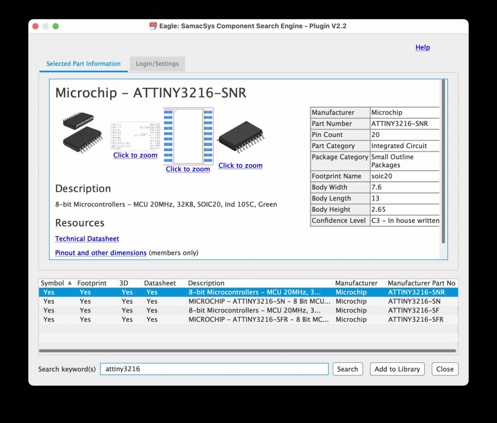
We have a choice of board designs and IC types, I choose the ATTiny3216 - mainly because I want to use the IC in subsequent weeks.
Here is the board:
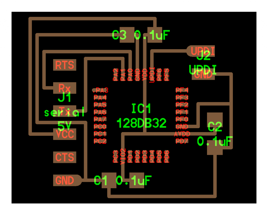
The challenge is now to redesign it, and add a LED and a Button.
Creating the Schematic
Now that EAGLE is set-up, we import the parts and name the connections according to the board:
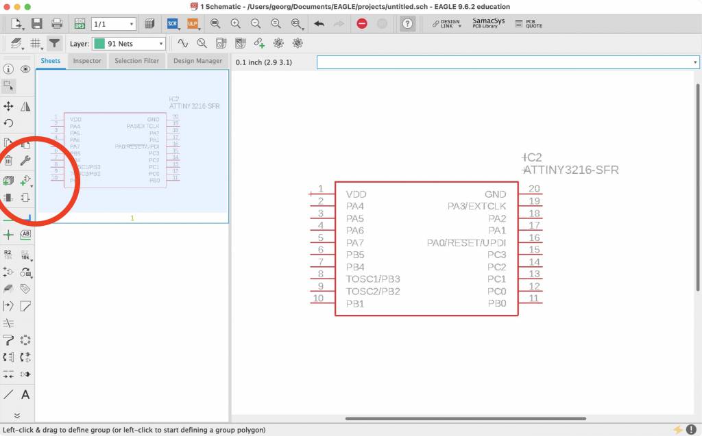
Add Button, add wire, name connection.
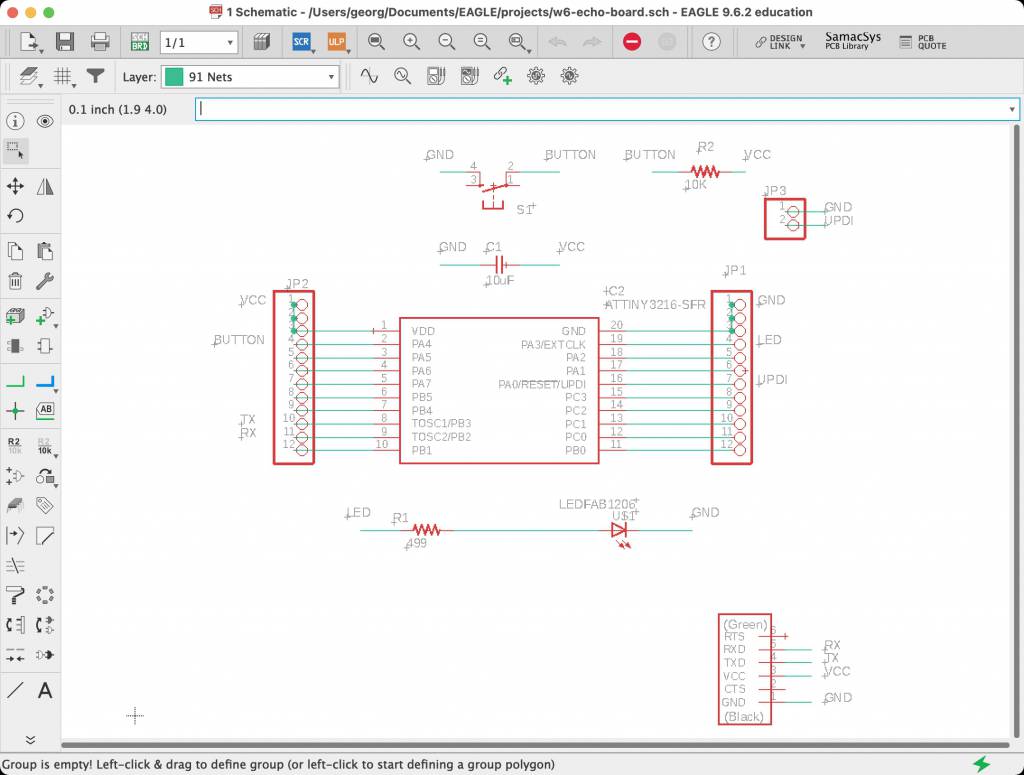
Naming can be done with the Naming button:
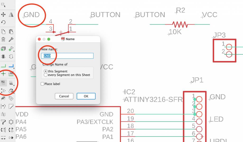
The position is not so important in SCH mode, we will take care of this the BRD mode.
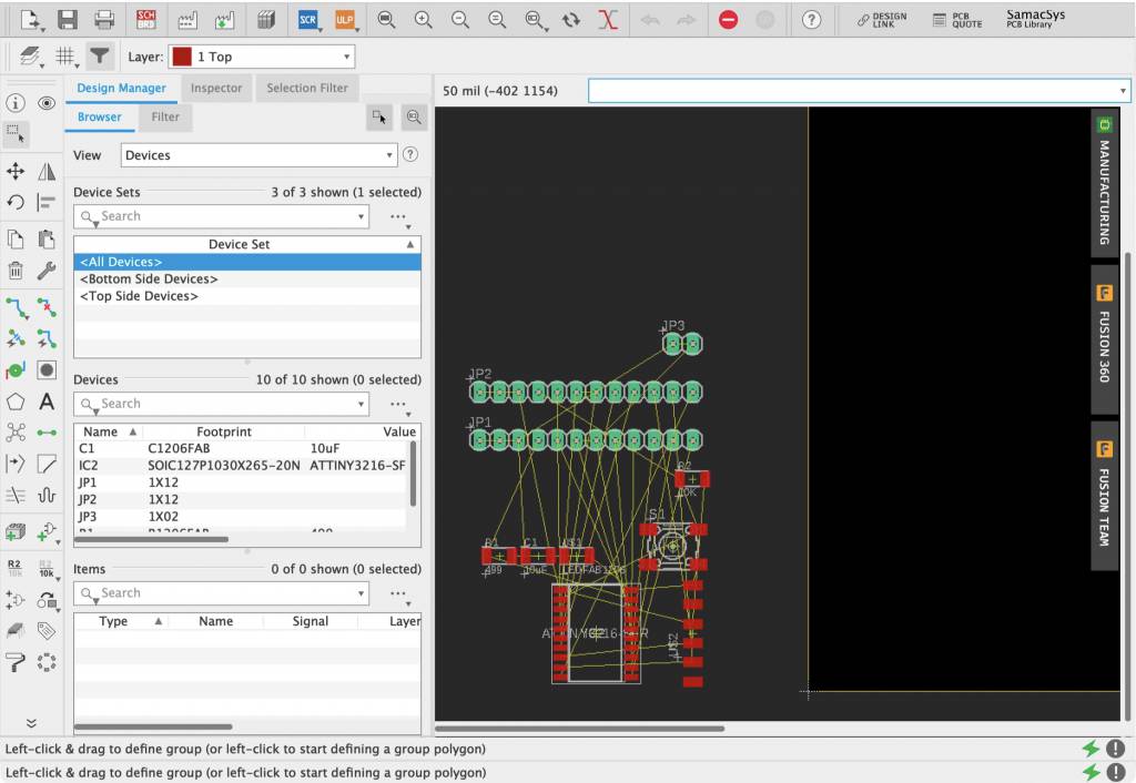
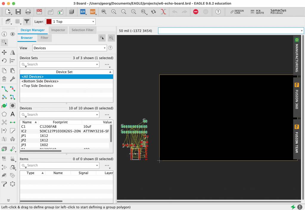
Routing the Board
After we are happy with the SCH, we switch to the BRD mode. And we are greeted by the Rat's Nest, the tangle of airwires and parts, by convention they are placed on the bottom left, outside the board.
Why is it called a rat's nest? Maybe/probably because it happens newborn rats unintentionally entangle their tails, create a nest of up to 10 or more individual rats, all connected through their tails. They can not move, but are kept alive by food from other rats. Also called a Rat King. Anyway.
Neil mentioned in his lecture, that routing itself is a playful exercise - and I can only agree: calming, quite relaxing, quite satisfying when you arrive at an elegant solution.
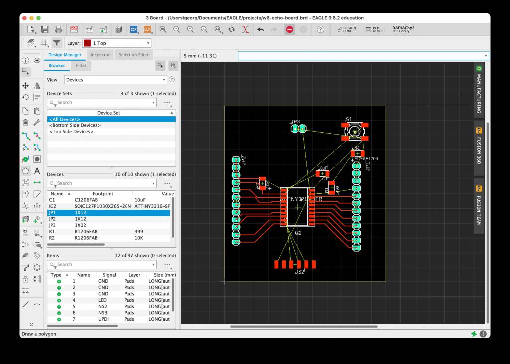
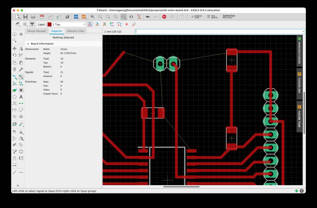
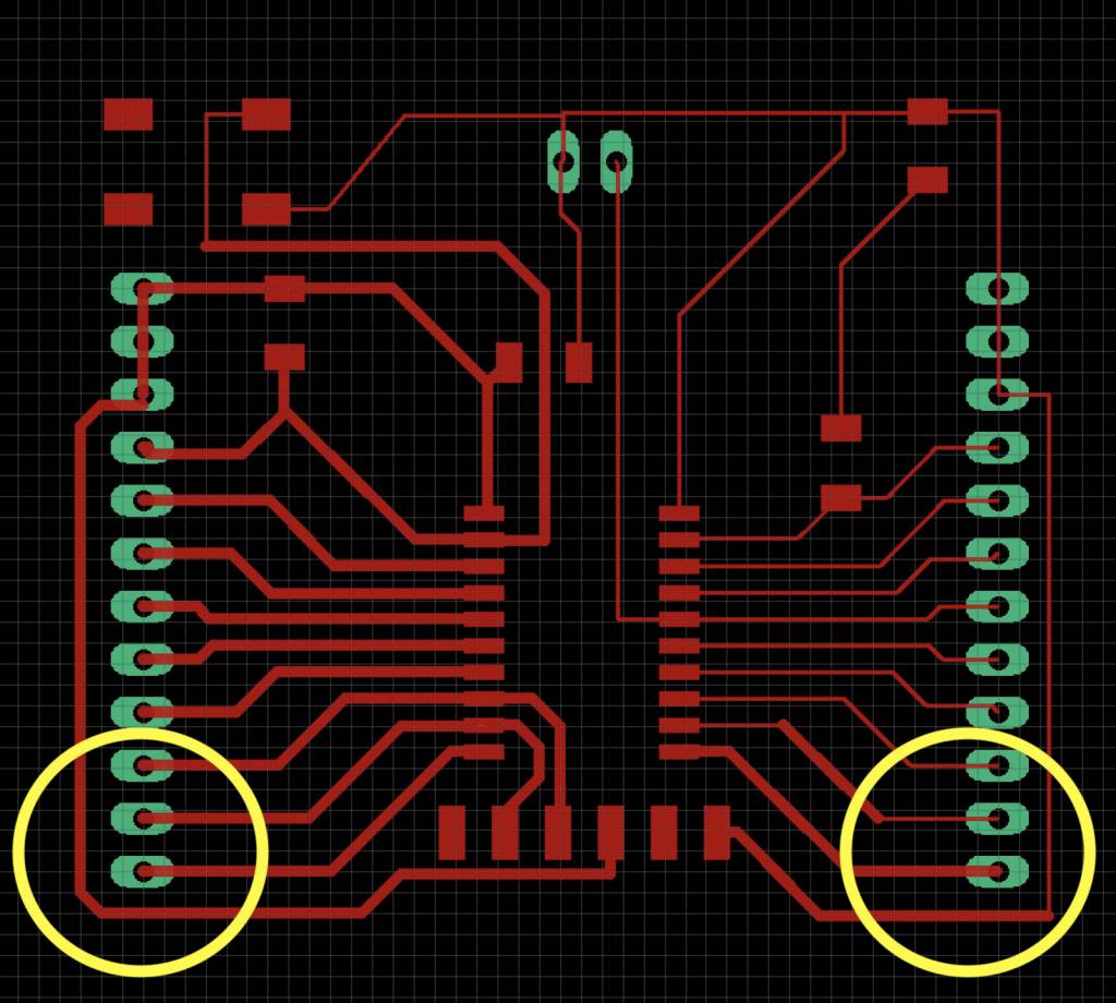
The right outside route was easy to rectify, re-routing under the IC and then connecting to the pad.
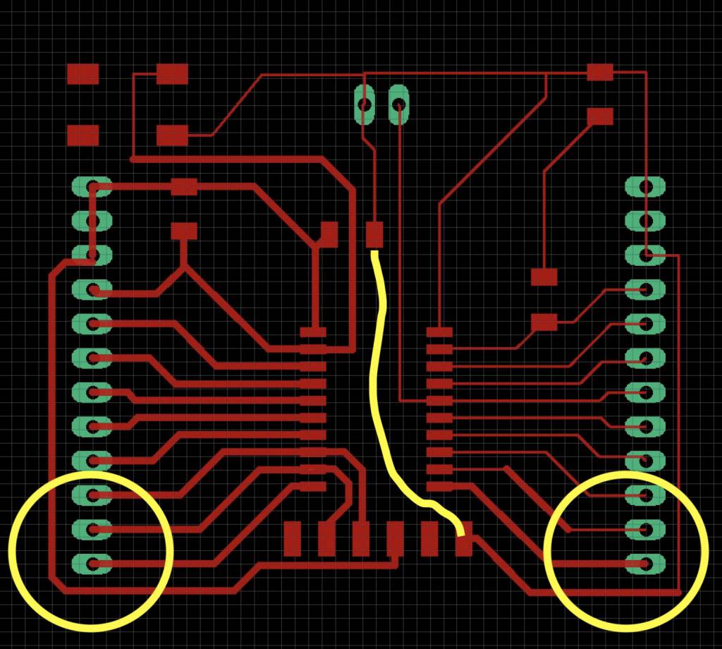
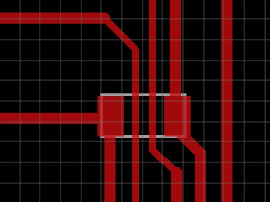
The left outside route was more challenging. I did not want to use a 0 Ohm jumper to simplify the design, so the only route was under the C1 capacitor:
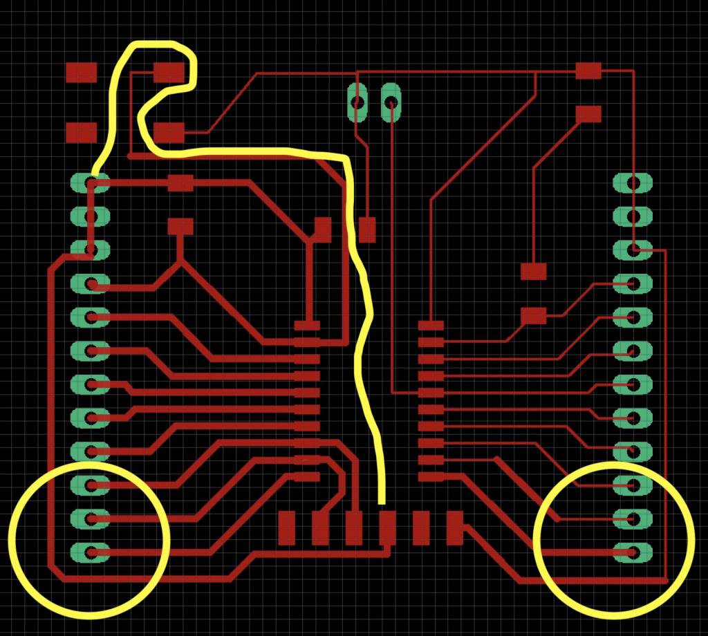
Double Routing with 0.3mm routes
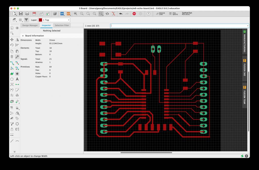
The final board. I made most of the routes 0.5mm except the ones underneath C1, they are 0.3mm.
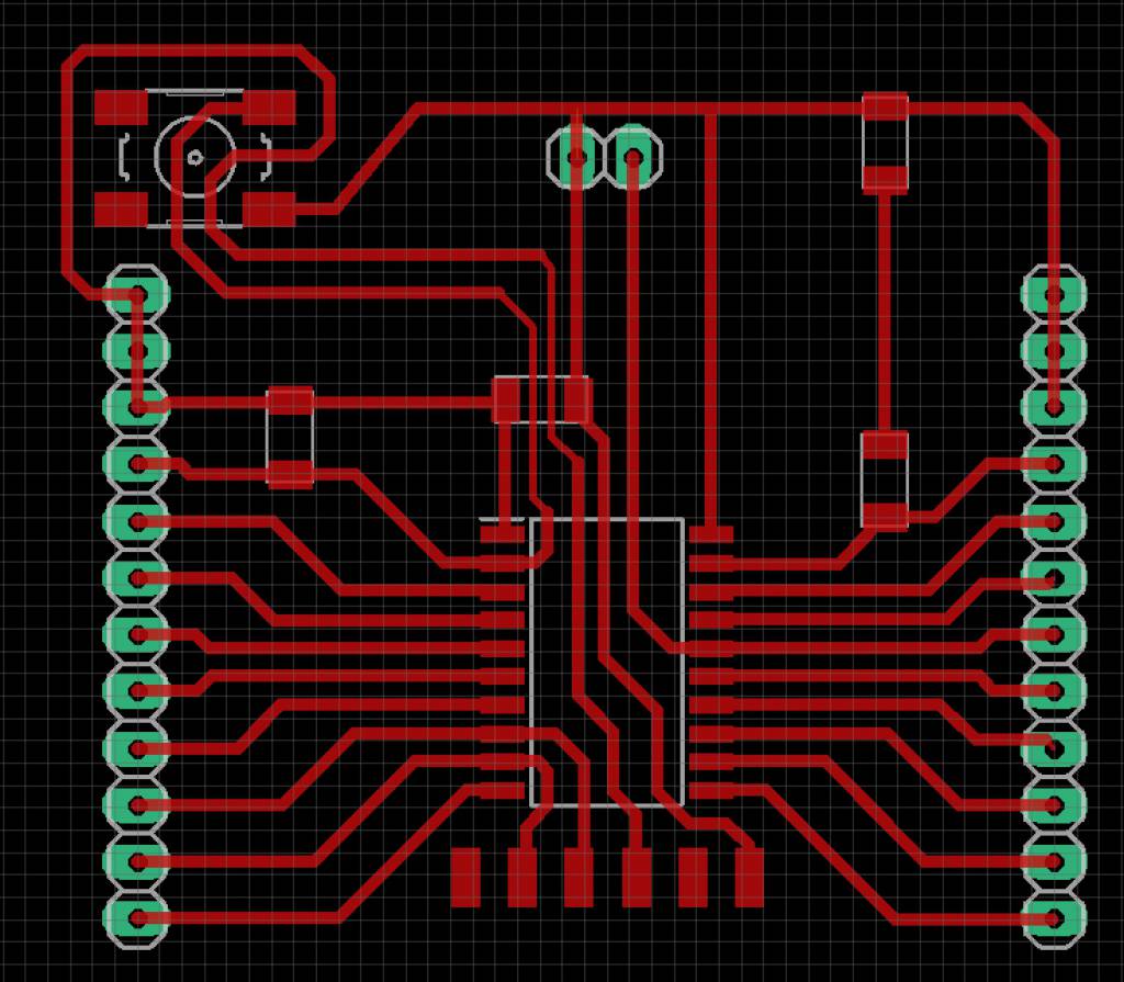
Exporting the Board
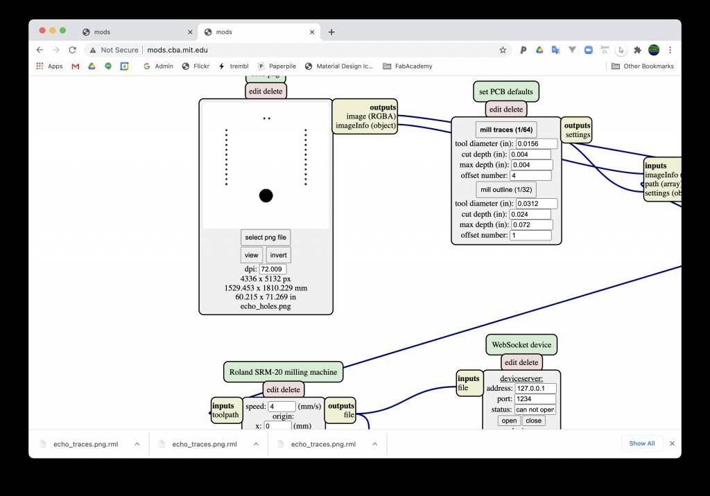
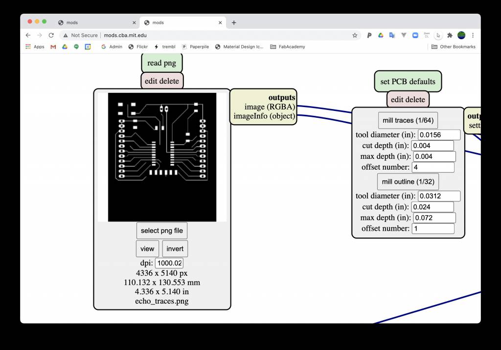
Once I was happy with the design, it's time to export the data for modding and then prepare it for milling.
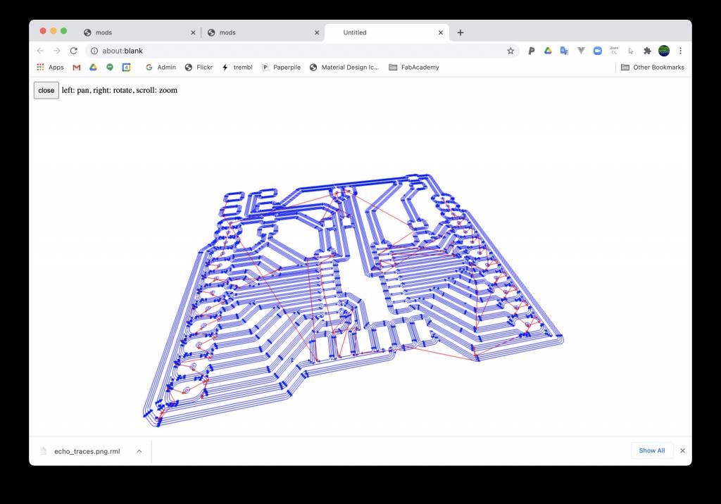
We actually need 3 different files for milling:
- Traces
- Holes
- Interior/Dimensions
Holes and Interior are separate files, because we can not guarantee that - were it one file - that the holes would be done before the interior - which could lead to unintended movement of the board which would lead to misaligned holes.
Why to we need holes at all? For the Pinheads, and - of course - the big centre hole to make the board fit into the Gameboy Cartridge.
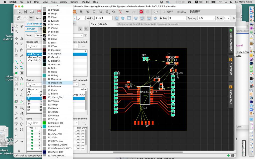
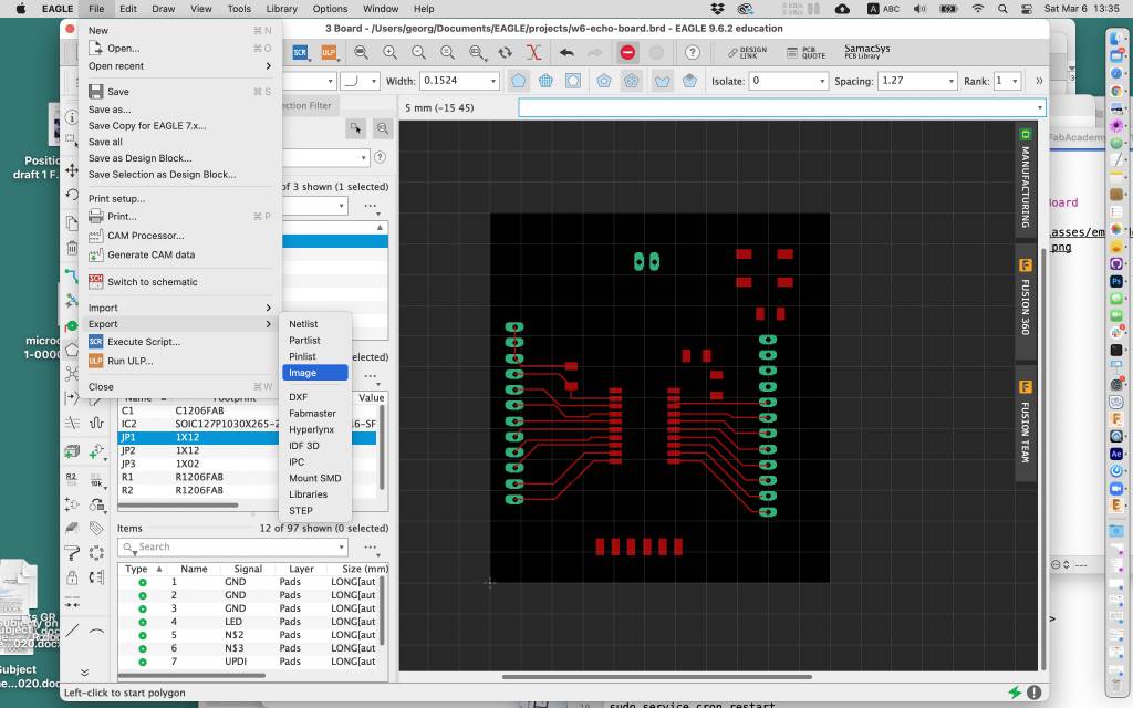
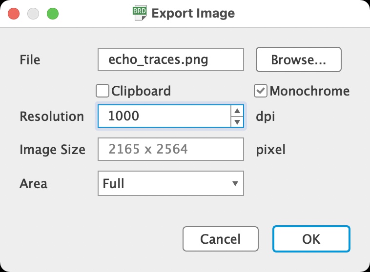
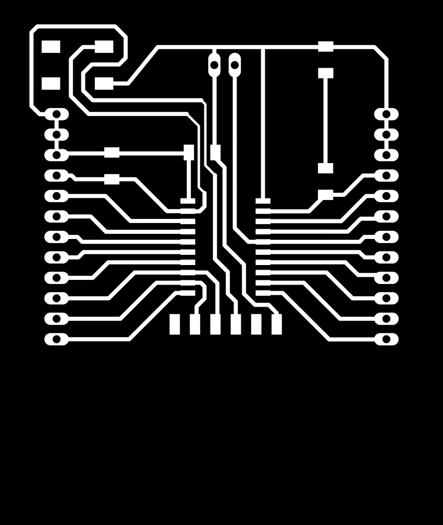
Exporting is done by selecting the appropriate layers, and then doing File > Export > Image.
- Traces: Layer 1 (Top) and 3 (Pads)
- Holes: Layer 45 (Holes)
- Interior: Layer 48 (Dimension)
Make sure to check the Monochrome box, and set dpi to 800 or 1000. The same value needs to be set in mods later.
That gives us the 3 png files for milling:
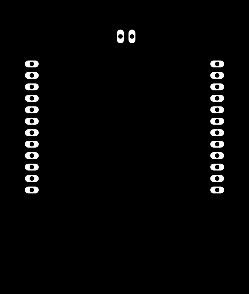

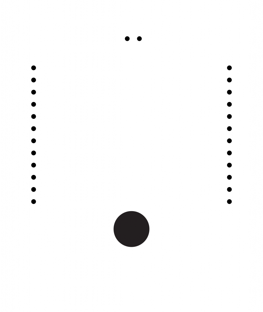
Ok. But wait a second. The holes don't look right...
Ok, that's better. (Harder to see the image, but better.)
Modding the Board
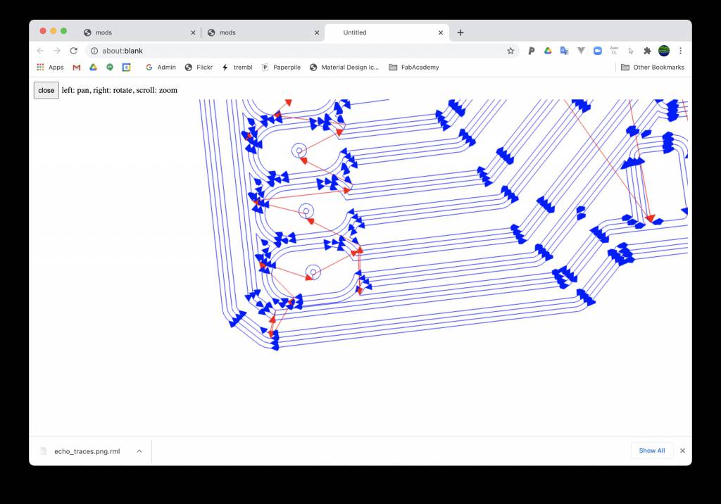
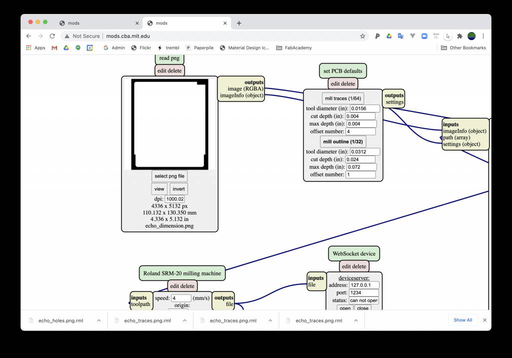
We do our usual dance with mods, select Roland SRM-20, add a save block, import the data, set the dpi, set the origin. (more details in my mods tutorial from Week 4). I need to look closer into mods, install a local version. I want to find out how to save a Patch locally. (excuse the Max/MSP Lingo).
But there is something new.
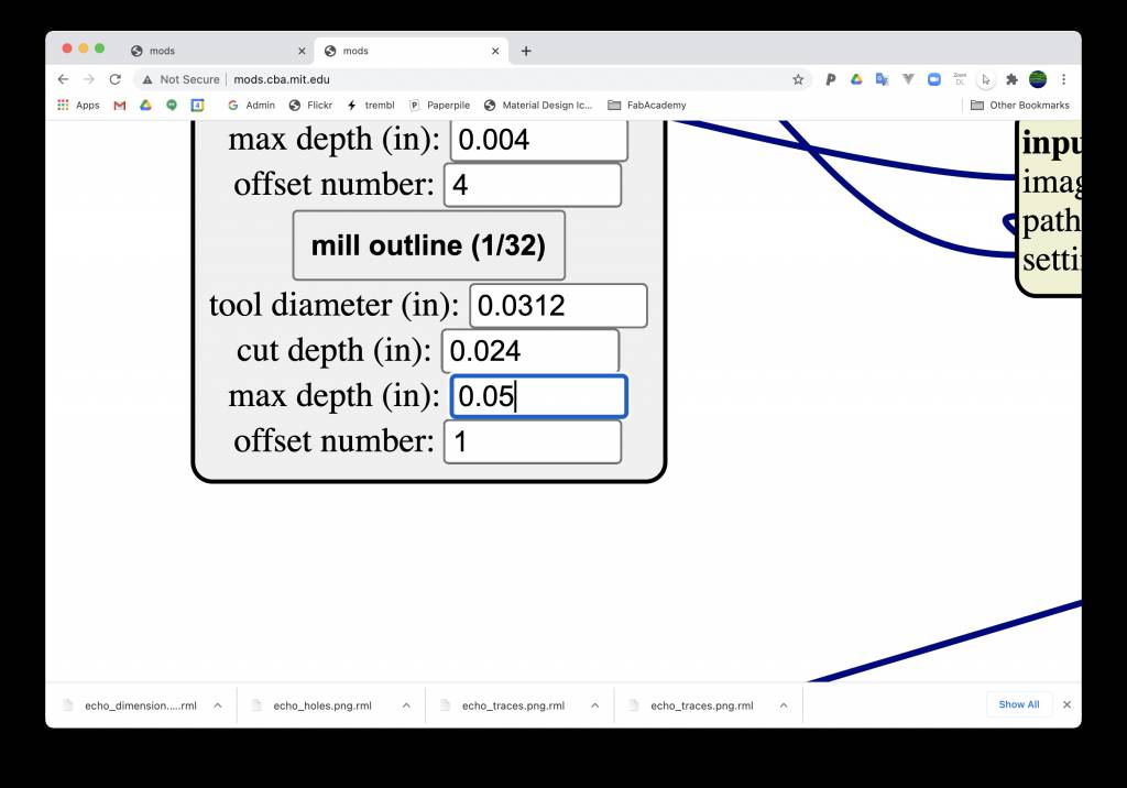
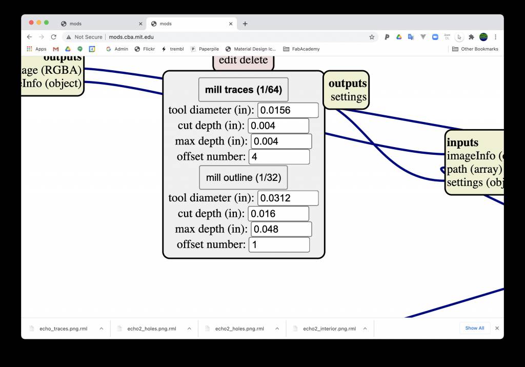
Because mods is making 3 passes on the board, the thickness be set in steps:
Mods

Paths
Changing Board Thickness
Default Settings for T1.8 board and 1/32 mill:
- cut depth: 0.024
- max depth: 0.072
It seems like max depth is cut depth * 3.
I changed it to:
- cut depth: 0.016
- max depth: 0.048 (~1.2mm)
It was cutting OK, but still into the sacrificial block.
Next time:
- cut depth: 0.014
- max depth: 0.042 (~1.0mm)
Milling the Board
Ready for milling. Or so we thought.
Asano-san's board were milling fine, when I started the process I got a strange, erratic behaviour:
Very frustrating. After doing, re-doing, and re-re-doing the mods procedure, I also tried to test cut Asano-san's file, which resulted is the same, erratic behaviour. And on the second SRM-20 too. Very, very frustrating.
The combined force of the Kamakura lab could not solve the problem, time was running out on Saturday.
Back on Sunday, this it was Nagano-san's turn in the lab. She immediately suggested that it might have something to do with the insertion depth of the mill bit in the mill socket (holder?), I inserted it too much, leaving no enough space for z-operations.
Another option was that switching on/off the power of the machines fixed it.
I wanted to find out the exact insertion depth when this behaviour was happening, but I triaged it aside to concentrate on finishing the assignment.
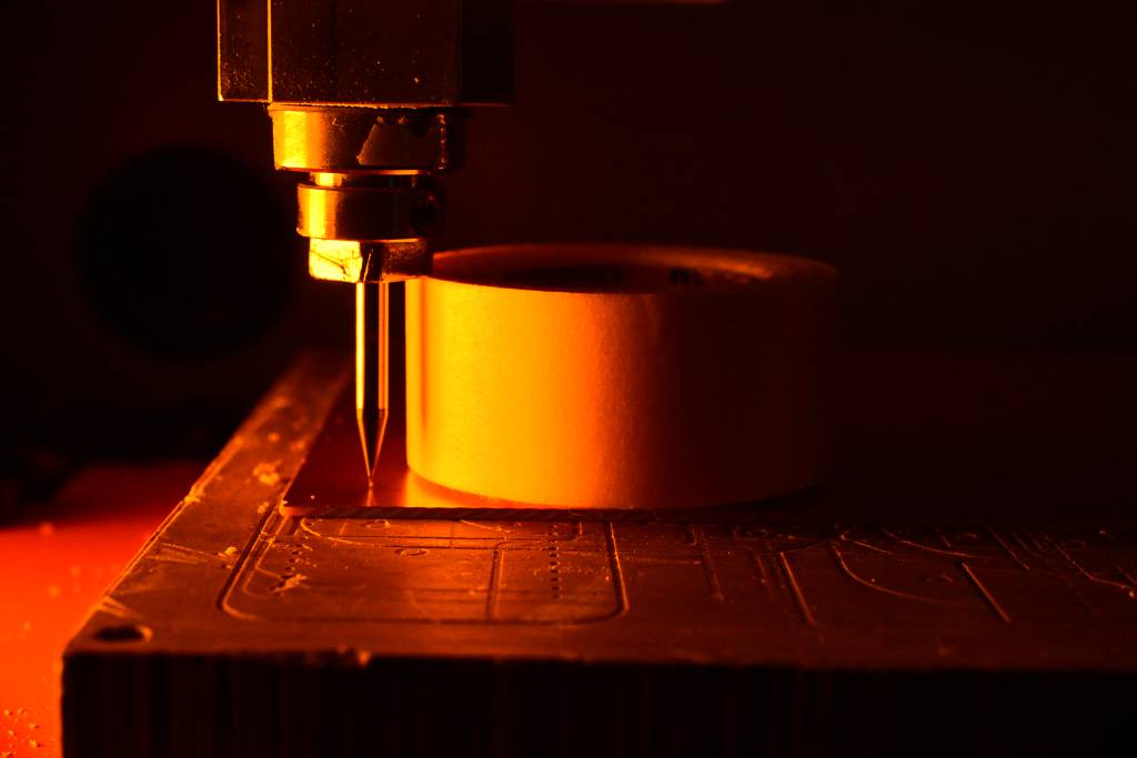
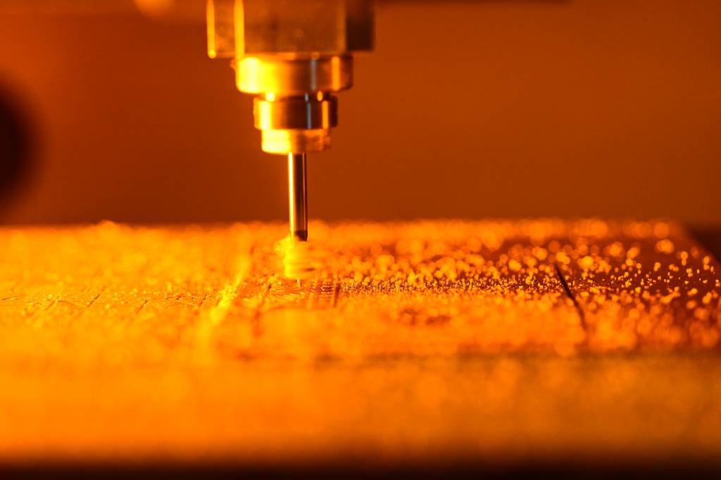
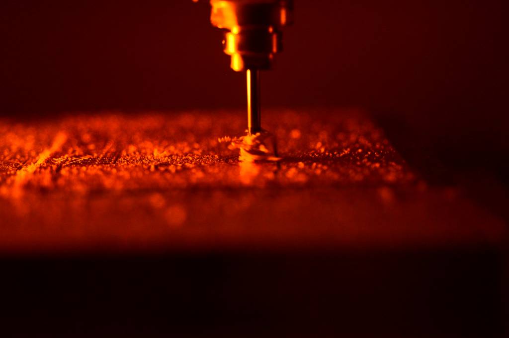
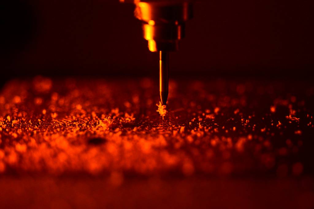
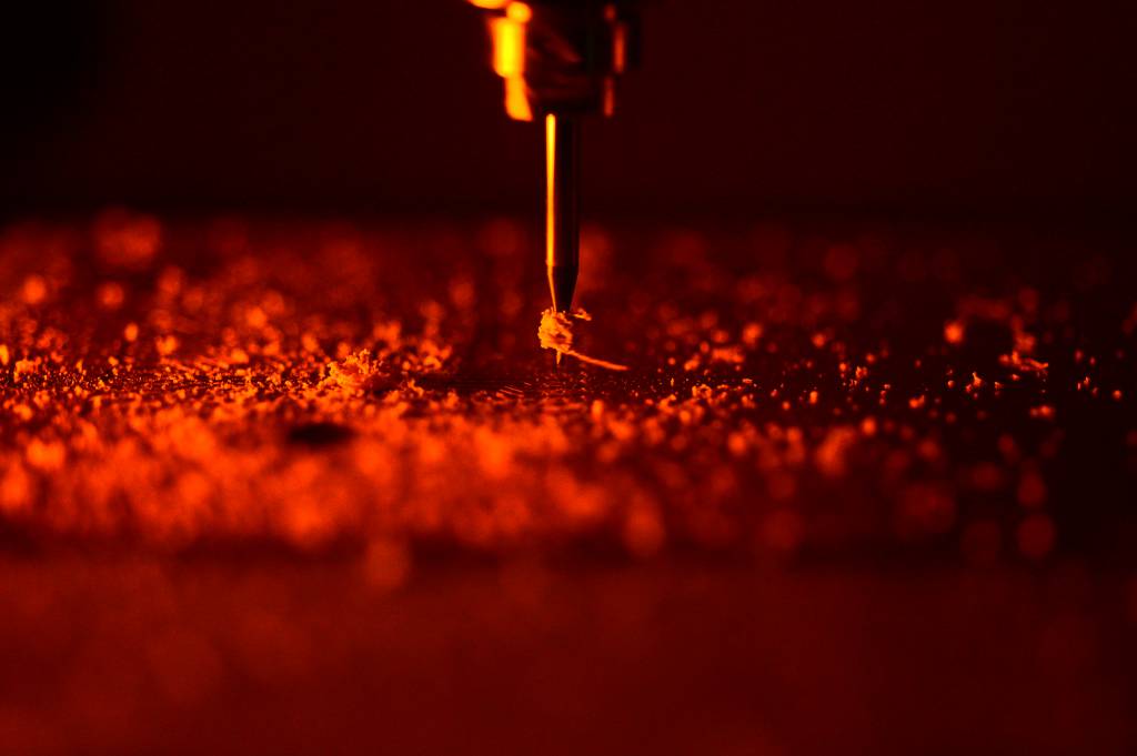
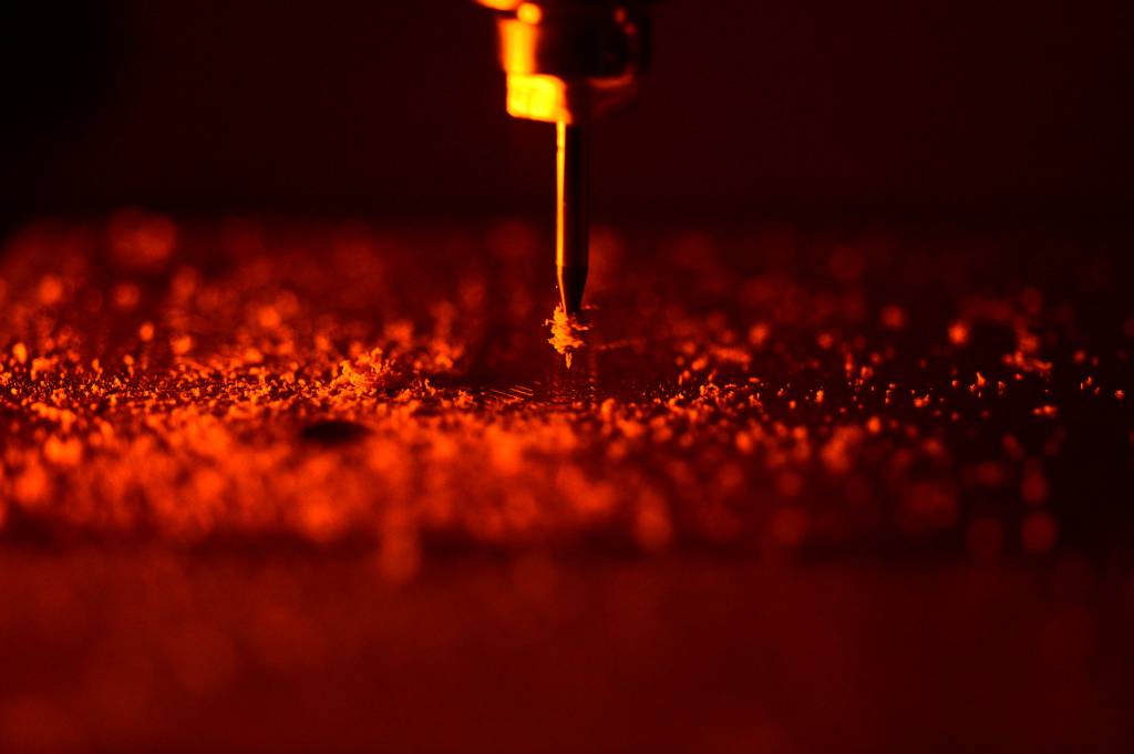
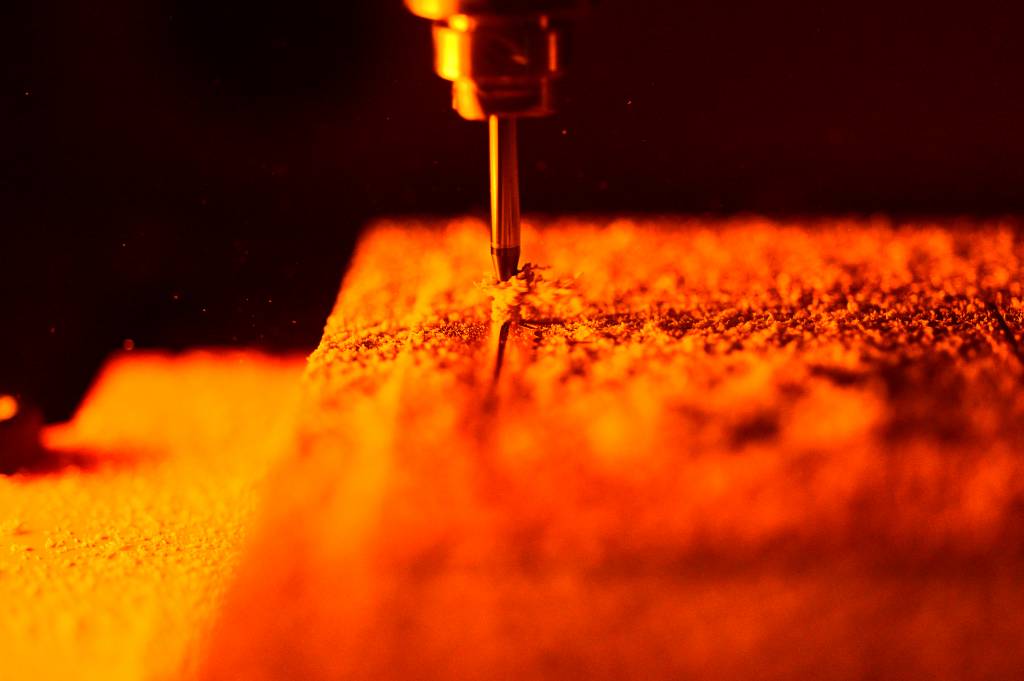
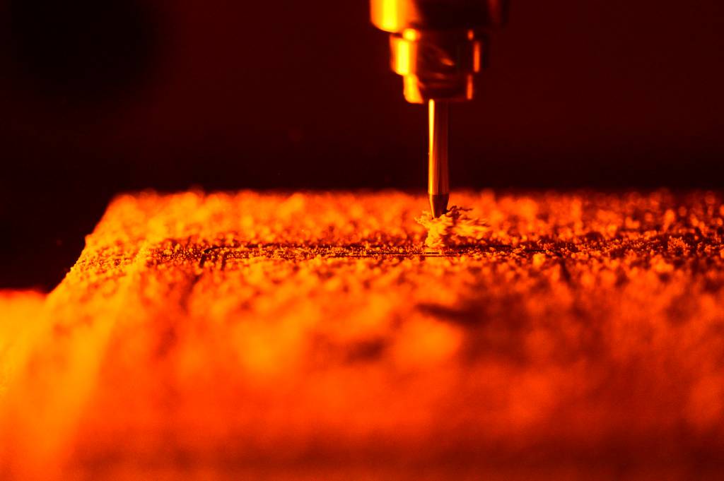
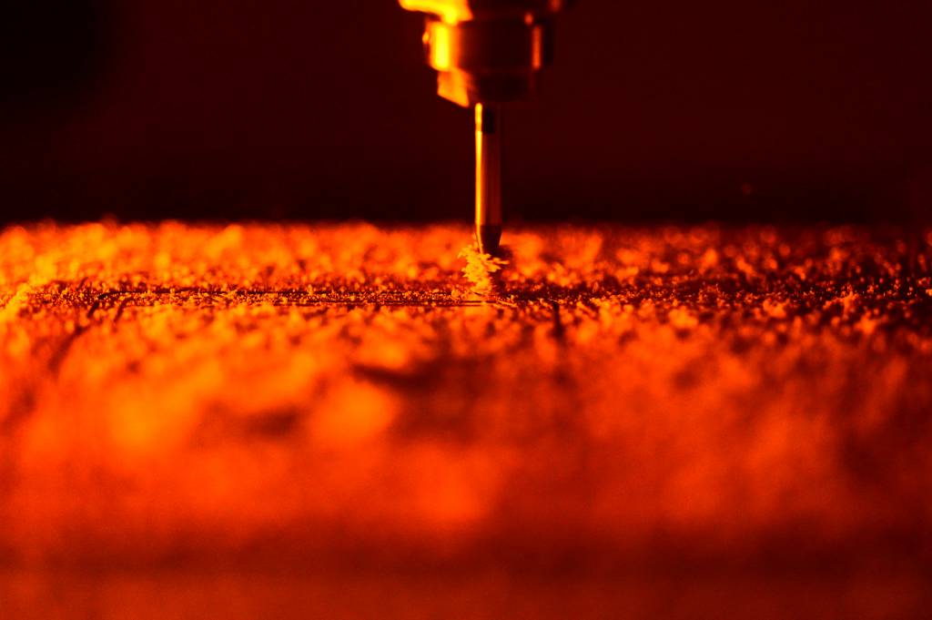
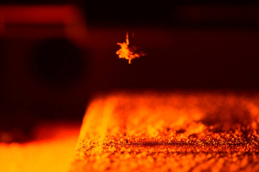
Now for real: Milling the Board
Some nice, relaxing, high-speed (1/8000s) images of milling-in-progress:
Populating the Board
Now that we finally have the board, onwards to populating and soldering. This should be more easy, as the pins are not as tiny as the FT230X from Week 4.
The only things I am slightly worried is the C1 capacitor - and the 2 routes underneath it.
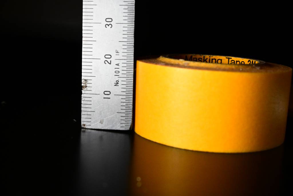
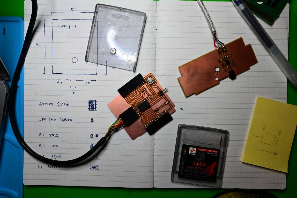
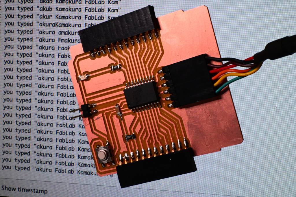
GameBoy Cartridge sized PCB
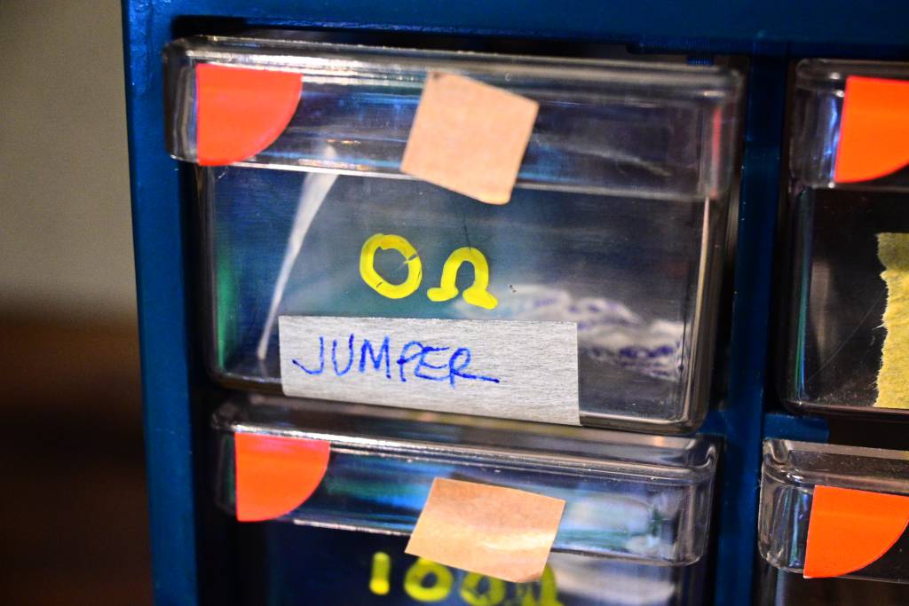
Parts Repository, including 0 Ohm Jumpers
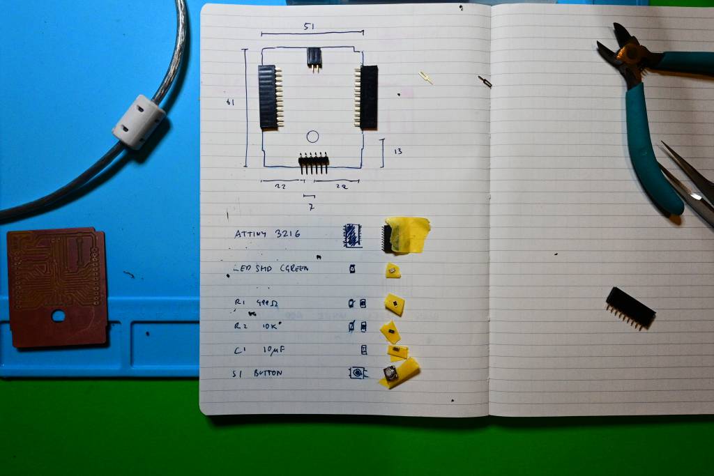
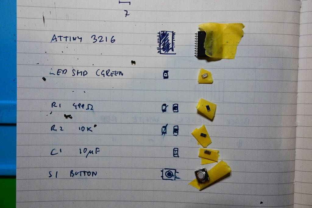
Notebook with Parts
Identifying Parts Orientation
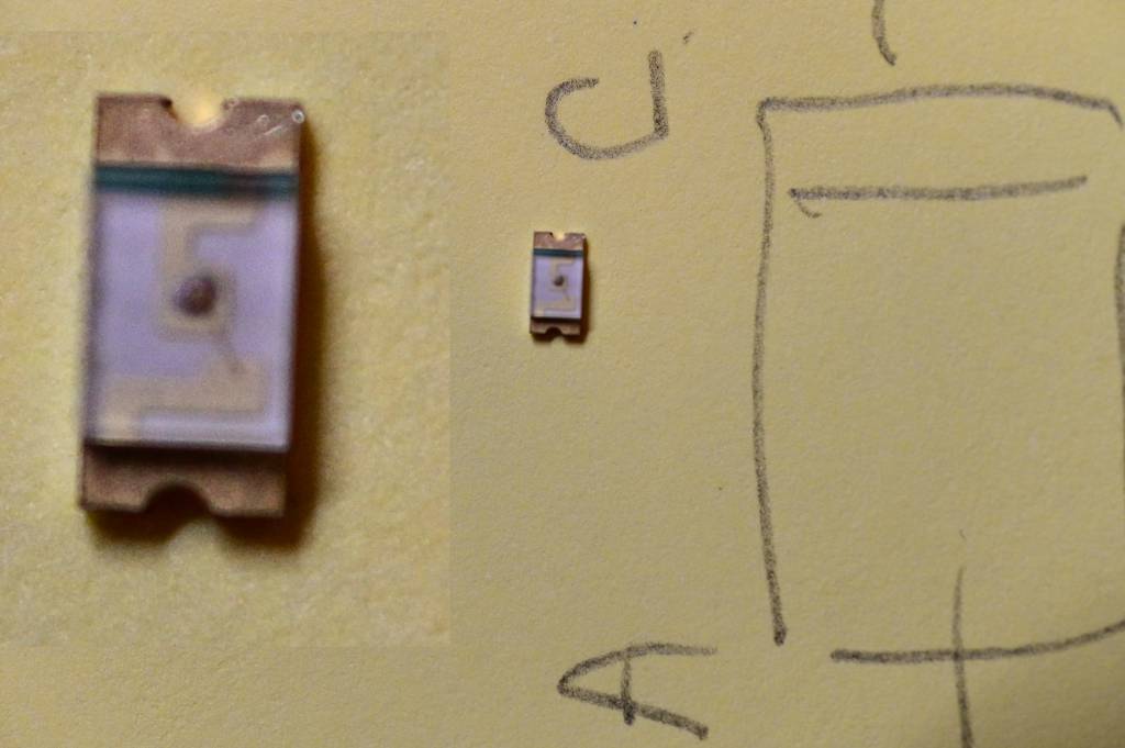
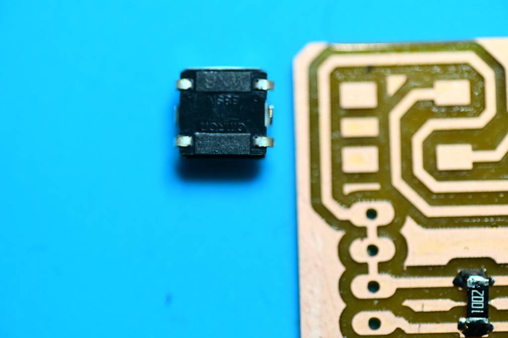
We learned to identify IC orientation by the dot on the left top. With LEDs it is usually easy, the longer leg is the anode (+), the shorter is the cathode (-). This becomes challenging with SMD LEDs.
SMD LED
Apparently there is (should be) a horizontal line at the cathode to identify it, but that was really, really, really, hard to see. Maybe because I choose a green LED. Nagano-san was again very helpful in clarifying that.
SMD Button
Buttons are easier to identify. When pushes, a current flows along the lines marked on the back.
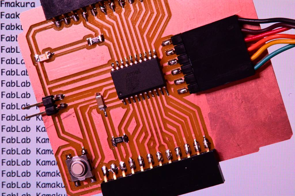
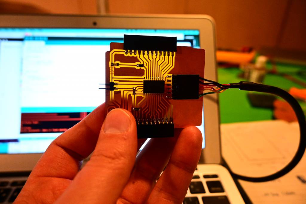
IC done!
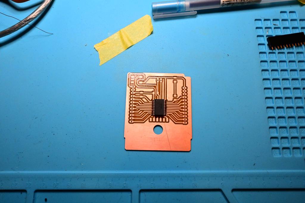
Board done!
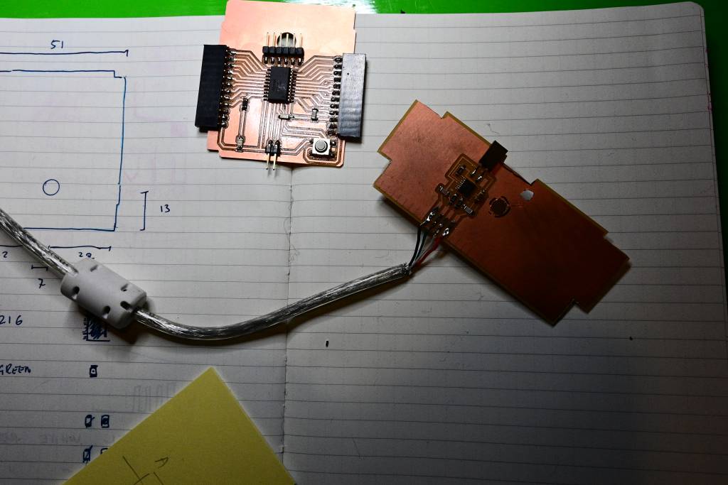
And being ready to connect with the Programmer from Week 4.
These boards very much feel like (and they are!) first attempts at Electronics Design and Production. I am looking forward to give it another pass and make it look and feel nice. But it works, and that's ok for now.
Demos
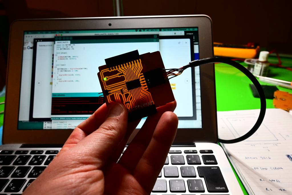
Echo Program
Connecting the programmer with USB, and the Echo board with a FTDI cable, they show up as serial devices. Yeah! Always happy to see this work!
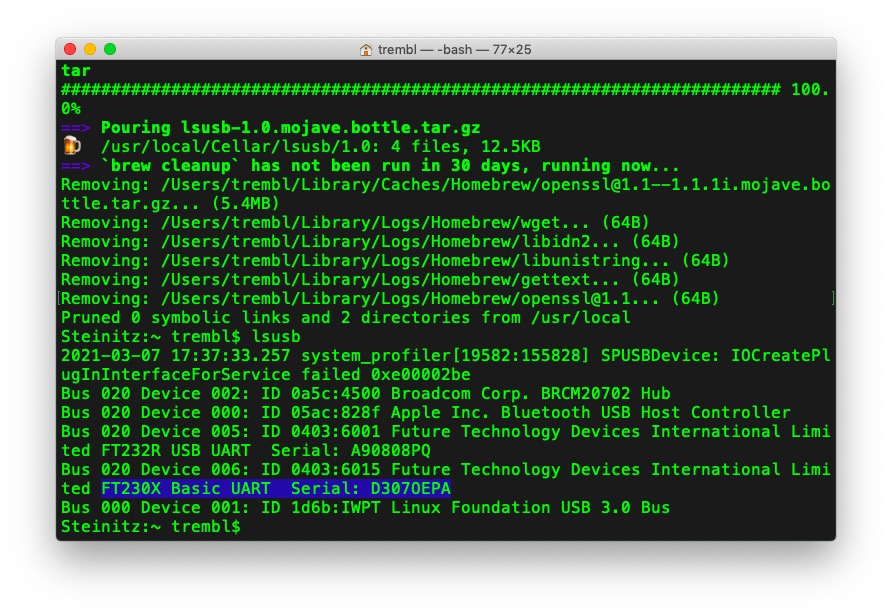
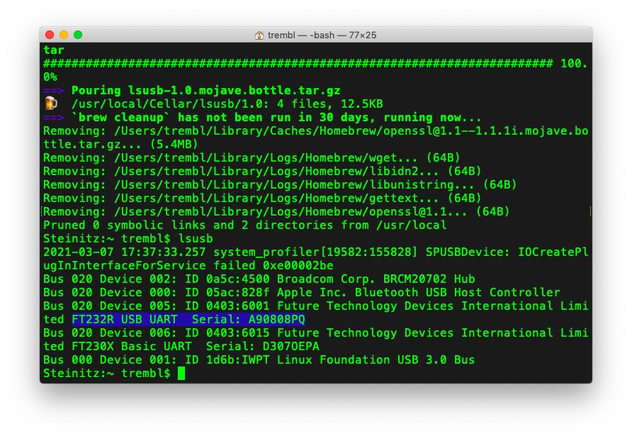
Running the Echo Script from the course site.
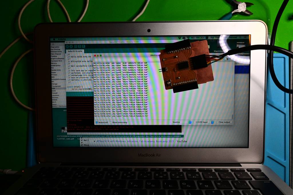
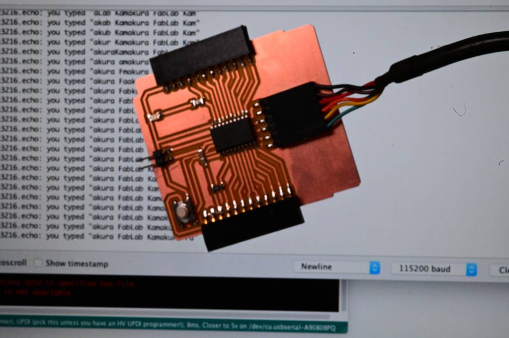
Great! That's working!
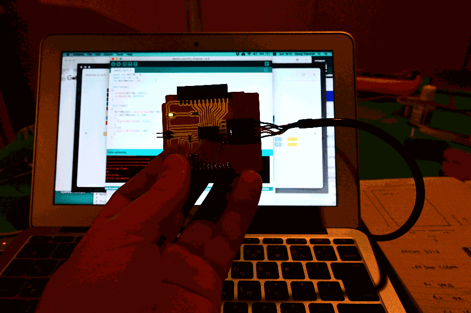
Very exhausted, nearly there, only one more thing to do. Will it actually blink?
Blink Program
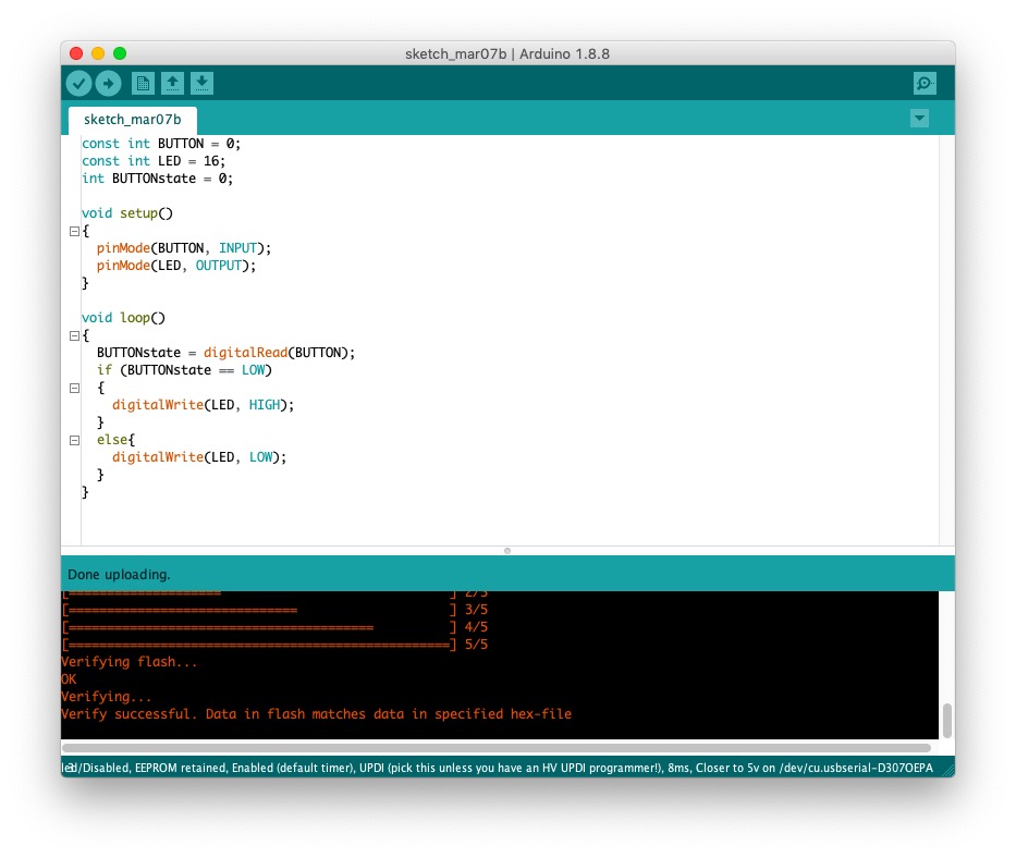
I made a quick blink program in Arduino, that listen to the input pin and sends a high/low to the output pin.
const int BUTTON = 0;
const int LED = 16;
int STATE = 0;

void setup() {
  pinMode(BUTTON, INPUT);
  pinMode(LED, OUTPUT);
}

void loop() {
  STATE = digitalRead(BUTTON);
  if (STATE == LOW) {
    digitalWrite(LED, HIGH);
  } else {
    digitalWrite(LED, LOW);
  }
}
The challenge was to make sure, which pins from the FT230X map the pins in Arduino.
A closer look at the ATTiny pin layout:
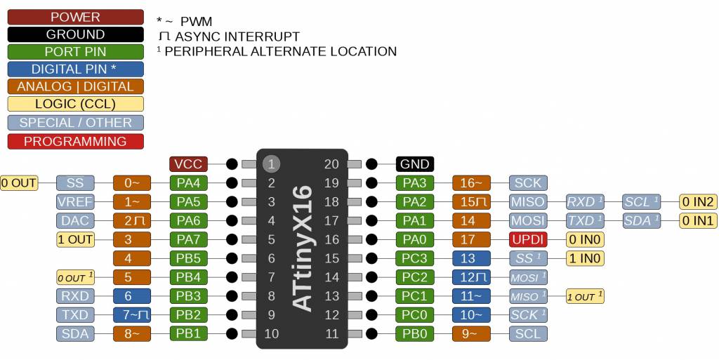
We can deduce:
- Port 0: Button
- Port 16: LED
Hero Image & Video
Blinken-GIF! (187K)
Learning Outcome
This week was a deep dive into circuit board design and production. The design process was not such a steep learning curve as I expected. It was wide, and shallow, but I got it to work, looking forward to dive deeper into it with sensor and actuators.