Weekly Summary
The week was all about communication. Communication between devices, between boards, how to send and receive data and messages. It was surprising to find out, that I2C devices don't have an agreed upon pin layout, almost all the I2C devices I got have different pin layouts.
I got around it by making a bespoke breakout board, as the idea of a universal, stackable I2C bus did not work.
Assignments
Individual Assignment
The individual assignment is to design, build, and connect wired or wireless node(s) with network or bus addresses. Assignment exegesis is slowly becoming a field on its own - what exactly needs to be done to fulfill the requirements of the assignment? Design and build refer clearly to design a board in Eagle, mill & stuff, then connect wired or wireless node(s) with addresses. The addresses is the important bit: Connecting devices to the A/D pins is not enough. With a view to the final project, I plan to explore the I2C and OneWire Protocols, to interface with Temperature Sensors, Displays and ToF Sensors.
Group Assignment
The group assignment is to send a message between two projects. We interfaced our respective 3216 boards with I2C, and send data from one board to the other.
If the temperature is over 24ºC, send an ON signal, if it is under 24ºC, send an OFF signal.
- Asano-san Board: LED
- My Board: I2C Temp Sensor and OLED
  if (tempsensor.readTempC() > 24.0) {
    Wire.beginTransmission(0x09);
    Wire.write(1);
    Wire.endTransmission();
  } else {
    Wire.beginTransmission(0x09);
    Wire.write(0);
    Wire.endTransmission();
}More code and details on the Networking & Communication Group Page.
Assignment Work Plan
This week feel into the so-called Golden Week holidays in Japan, which meant we could also use the lab on Tuesday and Wednesday. Here is the extended work-plan for this week:
- Saturday: Test I2C devices, mill & make break-out boards, communicate
- Monday: Akihabara, get more I2C and Sensors Connectors and Dev Boards
- Tuesday: Mill & make ESP32 dev board
- Wednesday: Documentation, Final Project Updates
Milling a Barduino 2.2 for developing the Final Project
I used a Barduino 2.0 ESP32 Dev Board that Jun made previously during the Electronics Week.
I wanted to start experimenting with my own board, and got the millable files from the Barduino 2.2. The difference from 2.0 to 2.2 is, that the 2.2 has a Micro USB connector on board (and the corresponding FT230 chipset), which means it can be programmed with a standard USB cable - a FDTI cable is not needed.
I downloaded the fabbable PNG files, and made some graphical changes that would remind me which position of the switch was for programming and running a program.

After that the mods dance.


The board has a mill-out for an antenna, which require slightly different settings:
Jun's suggestion was this:
trace anntena
endmill: 1/32
cut depth: 0.01 inch (0.254 mm)
max depth: 0.01 inch (0.254 mm)
offset number: -1 traceの内側をすべて切削する場合は-1を設定。(set to -1 to cut the entire inside of.)
The test-cut of the antenna worked fine, but when I milled the board #1, an emergency stop happened at the SRM-20. I reduced the cut-depth - and doubled the amount of passed needed for cutting out the antenna rectangle.
cut depth: 0.005 inch (0.127 mm)
max depth: 0.01 inch (0.254 mm)
offset number: 0 (0=fill)
ESP32 Board: Attempt #1
Here is the first attempt:


Intermission


ESP32 Board: Attempt #2


Not wanting to discard the board, I am attempting to use the sonic knife to sever the trace connection:


ESP32 Board: Attempt #3


Another round of milling:


Next step. Stuffing and Testing. And running out of time to do this extra work this week. 🤨 Back to the week's assignment.
Communicating with I2C
I2C Work Plan
- Test Devices on Arduino Uno
- If it works, test on ATTiny 3216
- If it works and ESP32 is done, test on ESP32
I2C Device Line-Up
| Name, Type | Voltage | Price* | Address | Pull-Up? | Pin Order | Link & Datasheet |
|---|---|---|---|---|---|---|
| LCD Module, 16x2 Display | 3.3-5V | ¥645 | ? | ? | Multiple Pins, Backlight, etc | Akizuki, How To |
| 0.96 OLED, 128x64 P-1580 | 3 - 5.5V | ¥580 | 0x78 (0x7A), found: 0x3C | Internal | GND, VCC, SCL, SDA | Akizuki |
| 0.96 OLED, 128x64 P-12031 | 3.3 - 5.5V | ¥580 | 0x78 (0x7A) | Internal | GND, VCC, SCL, SDA | Akizuki |
| ADT7410 Temperature Sensor | 2.7 - 5.5V | ¥500 | 0x48 (0x49, 0x4A, 0x4B) | Internal, jumper not soldered | VDD, SCL, SDA, GND | Akizuki |
| VL53L1X Laser Time-of-Flight | 2.3 - 5.0V | ¥1320 | 0x52 | ? | V+, GND, SDA, SCL | Akizuki |
- Price as of May 2021, incl. tax.


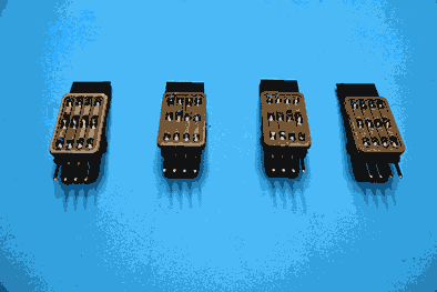
Making Connectors for the I2C Devices
Chronologically I did this before looking closely at the I2C data sheets. The connectors did not work - well, they worked - but because each I2C device had a different pin assignment, they were not really useful. But I believe the animations are too nice to not include them here.


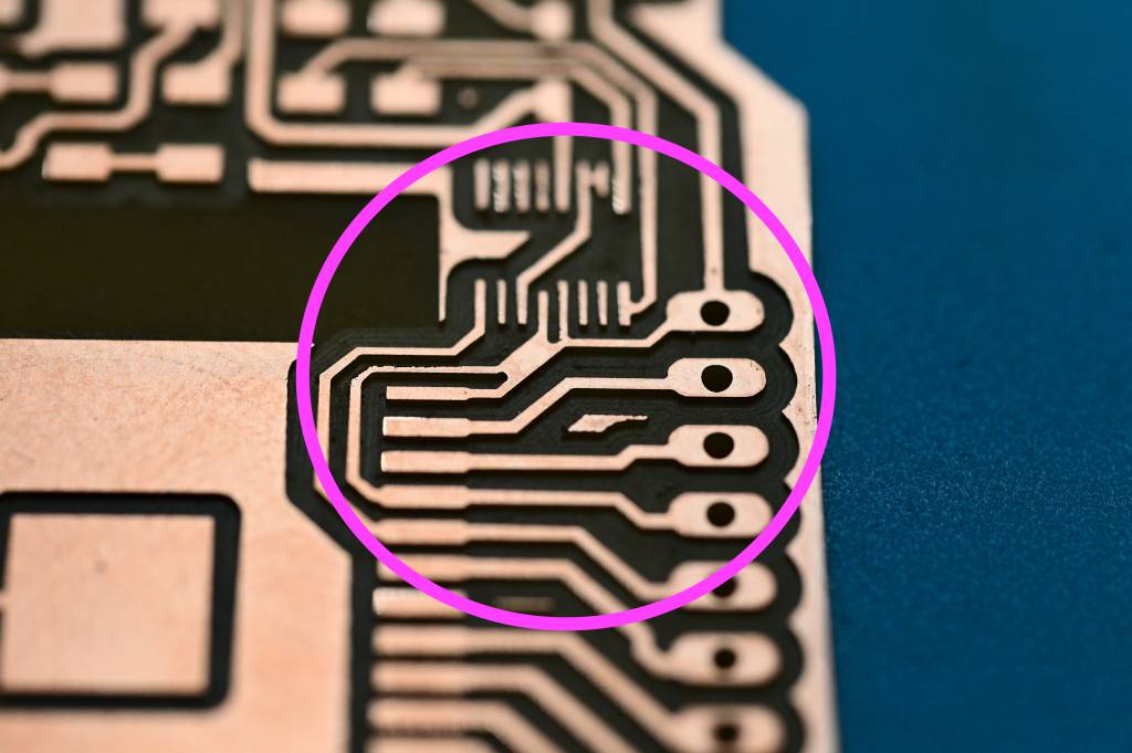
Pull-up Resistors? Why are they needed?
Understanding the concept behind pull-up resistors took me a little while, the explanations from this tutorial helped immensely, especially these illustrations:


Testing I2C with Arduino


Testing I2C with my ATTiny 3216
I made a bespoke board to fit the different pin configuration for the temp sensor and the OLED display. First time I had to cheat and use a 0K resistor.


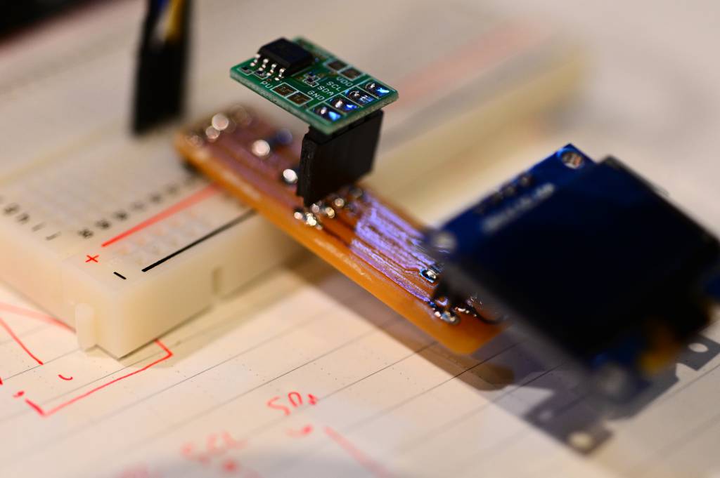


The board in Action:
I2C Addresses: 7bit and 8bit
hex: 0x78, binary 8bit 0111 1000When the last bit is ignored, the address becomes a 7bit address:
hex: 0x3C, binary 7bit 011 1100References
-
Paul Watzlawick: Man kann nicht nicht kommunizieren. Cmp.: Menschliche Kommunikation – Formen, Störungen, Paradoxien. (Originaltitel: Pragmatics of Human Communication. A Study of Interactional Patterns, Pathologies, and Paradoxes. W. W. Norton & Company, New York 1967.)
-
Monochrom: Nicht nicht kommunizieren gilt nicht! , Nettime Mailing List, Wed, 9 Apr 2003 08:20:52 +0200 https://nettime.org/Lists-Archives/rohrpost-0304/msg00076.html