15. Networking and communications
Introduction
This week, we were assigned two different assignments, with one being an individual assignment, and the other a group assignment. The individual assignment for this week was to design, build, and connect wired or wireless node(s) with network or bus addresses. The group assignment for this week was to send a message between two projects.
Individual assignment
This week, I started off with the individual assignment as usual, since we were stuck at home due to the pandemic. The first thing that I did was that I looked through the different types of communication, and looked through what people in previous years had completed. I came across several types of communication on each page, but some of the examples that I saw were I2C communication on Katie Chai’s Page. I decided that I would create a modified satshakit, similar to Katie Chai, as I figured that it would be good for future use in my final project as well. To start off, I looked at the satshakit webpage on the Fab Academy page, which had all the information on the background, what it is, how to make it and the schematic and board files. I read through the page to fully understand how the satshakit was, and I am really glad that I was linked to this source.
The ATMEGA 328
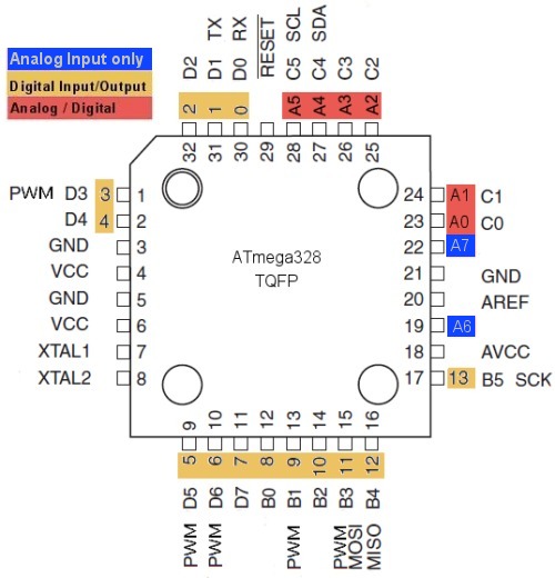
Like the Arduino UNO, the Satshakit uses the ATMEGA328 microcontroller, which I decided to do some research on, as I did not have any previous experience with it. The first thing that I did was that I looked at the pinouts in order to see what I could use for my final project. I came across this image which was very helpful as it showed all of the pinouts
After viewing the pinouts, I looked at the datasheet for the ATMEGA328, which I skimmed over to get some general idea of the chip. I then went back to the fabacademy page for the satshakit in order to download the schematic and the board.
Modifying the board in EAGLE
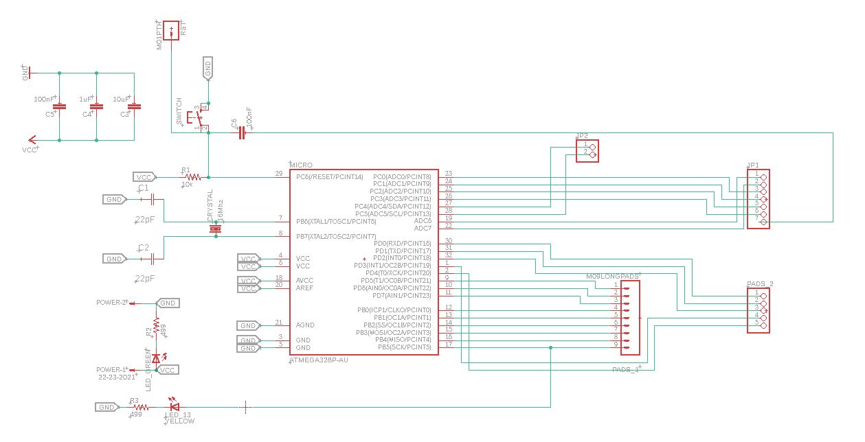
After I downloaded the schematic and board I went on EAGLE to modify the design. Since I was using I2C communication for this week, I decided to move the I2C pins separately as it would be easier to access and will be easier to identify. Here is what my schematic looked like after I made my changes
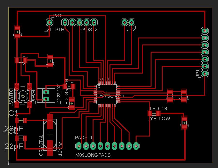
Although I would usually autoroute a board after I switch it over to the brd mode, this time since placement is key, I manually routed each trace. After a little while of trial and error with paths, I eventually ended up with this arrangement.
Milling the board out
After modifying the board, I saved the board file, and I tried to open the file on Bantam, but some of the pads were not showing up like this:
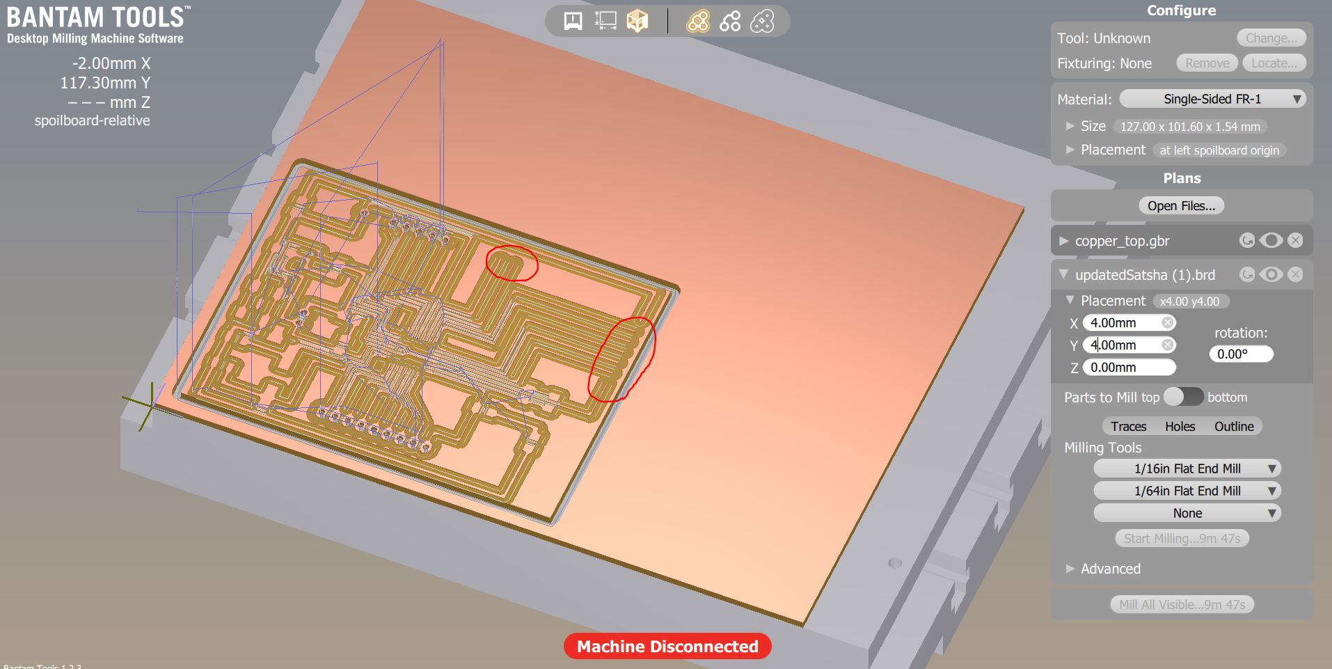
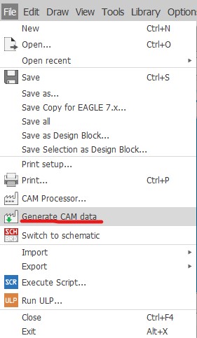
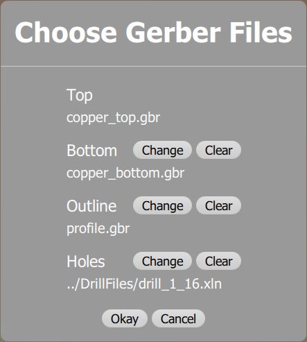
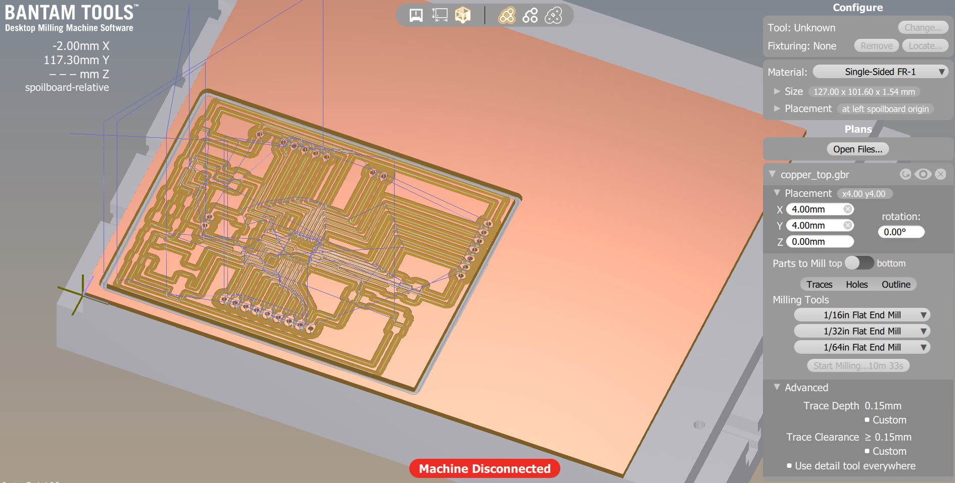
I realized that I had to save the board file a different way. The way that I approached this issue was by simply saving the brd file by going under file, then clicking generate CAM data. Once this was done, a zip file was saved to my computer, which I unzipped. In that folder are the Drill Files and the Gerber Files which I opened using Bantam. This is what that setup screen looked like:
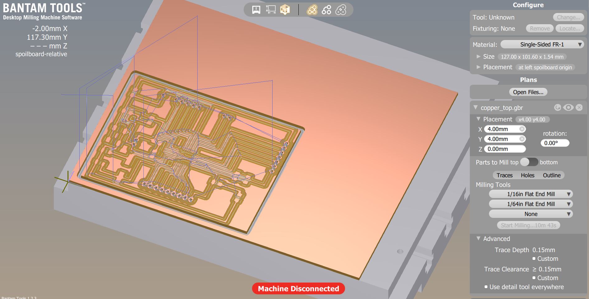
After my board file was complete, it was time for me to mill out my board. I milled out my board using a 1/64th bit for the traces and a 1/16th for the outline. Here is how I set up my board in Bantam.
After the board was milled out, I sanded it a little bit and then stuffed it, and here is how it turned out:
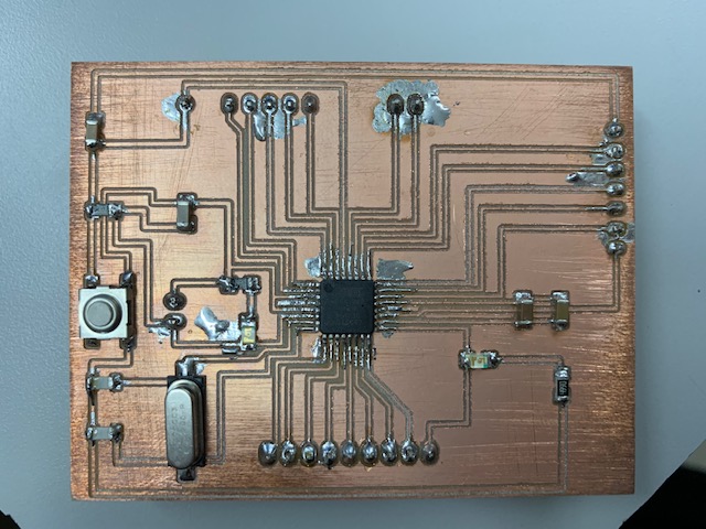
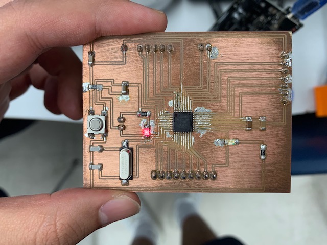
After everything was complete, I went over to burn the bootloader on the board, but I was not able to do it, and I realized that it was due to the small copper bits that were caught between my traces. Initially, I didn’t think it wouldn’t be much of a problem, but after grabbing a multimeter and running a continuity test, I realized there were small shorts created throughout the board. I realized that the best solution to this issue was to simply re-mill the board, but this time, used three bits (1/16th, 1/32th, 1/64th)to mill the board (I later realized I could just go under advanced and set the trace clearance higher, which I started doing from this point on). After setting everything, I milled out the board, sanded it, checked if there were no copper pieces in between the traces (which there weren’t) and then I stuffed the board. Here is how it turned out:
Now it was time for me to burn the bootloader on my new board.
Burning the Bootloader
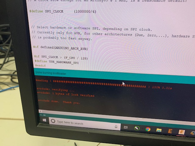
After everything was set, I opened Arduino and referenced the satshakit website in order to see the diagram below, which shows how I should wire everything up in order to burn the bootloader. Once everything was wired, I got clicked the burn bootloader button in Arduino and it worked!
Testing example code
After I got the bootloader on the satshakit, I decided to try some example code, and opened the blink example on Arduino. I uploaded the code, and here is how it turned out:
Master-Writer, Slave Reader test on Arduinos
After I tested my satshakit, I proceeded to the I2C part of this week. I decided to finally run the Master-Writer, Slave Reader Code on my satshakit to accomplish this week’s goal. The information that I followed came from the Arduino Website. This tutorial showed me how I would need to wire two boards together and also provided the code for both the master and slave boards. Before I tested this on my satshakit, I wanted to try it on two Arduinos so that I would know that it works. I got two male-to-male jumpers, and hooked them up as stated, and uploaded the master code to one Arduino and the slave code to the other. The program is supposed to make the master send 6 bytes of data every half second to a uniquely addressed slave. To make sure this works, messages should be displayed on the serial monitor of the slave device. The code prints “x is ” then the value of x increases every time. Here is how it turned out:
Master-Writer, Slave Reader test on Satshakit
After I knew that my board was functional and that the code was functional for the master-slave program, I now used my satshakit in order to act as the master board and an Arduino UNO for the slave. I uploaded the code to each and opened the serial monitor and the I2C communication between the two boards was working!
Summary
This week, I learned about how to get two boards to communicate with each other, and although I decided to go with I2C communication this week, I thought it was really cool that there are so many ways of communication. I would definitely like to try different types of communication, hopefully, something wireless, as I already got to work with a wired type of communication this week. I think that this week has been the hardest week so far as I took in a lot of information that I had no previous knowledge on, but I enjoyed doing it.
Group Project
Here is the link for the Group page for this week
Files
Here are all of my files for this week. Files