Week 7: Electronics design
Do you know the rule of organizing your work? The earlier the better! How does it work in reality? Usually doing something later is "the later". I think milling machines were never so much occupied. Well, I have strong feeling that probably last year, around same time could compete. Anyway, positive side was that we could all complain a bit on same issues and solve them together.
Okay, we mostly focused on complaining.

Group Assignment
"This time group changed a bit: I joined Marjo and Michael
It is a bit weird but in a moment, when I'm writing it all the work for Personal assignment is already done and proven working. We had to use test equipment to observe operation of the board. There are couple tools we could use (most suitable in bold):
- Multimeter
- Putty - telnet client
- Oscilloscope
Obvious choice is oscilloscope and Putty (via FTDI) cable in order to see some communication. Baud rate of terminal was 115200. Below proper connection of the oscilloscope' probe, ground connected with crocodile connector and quite fragile pin to pin connector (as long as someone hold it - works).
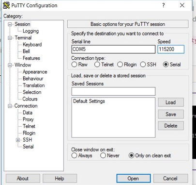
Putty client should be properly configured. From Connection type/Serial tab, serial line and baud rate has to be adjusted: Serial line/COM5 and Speed/115200. Then finally it could be Opened
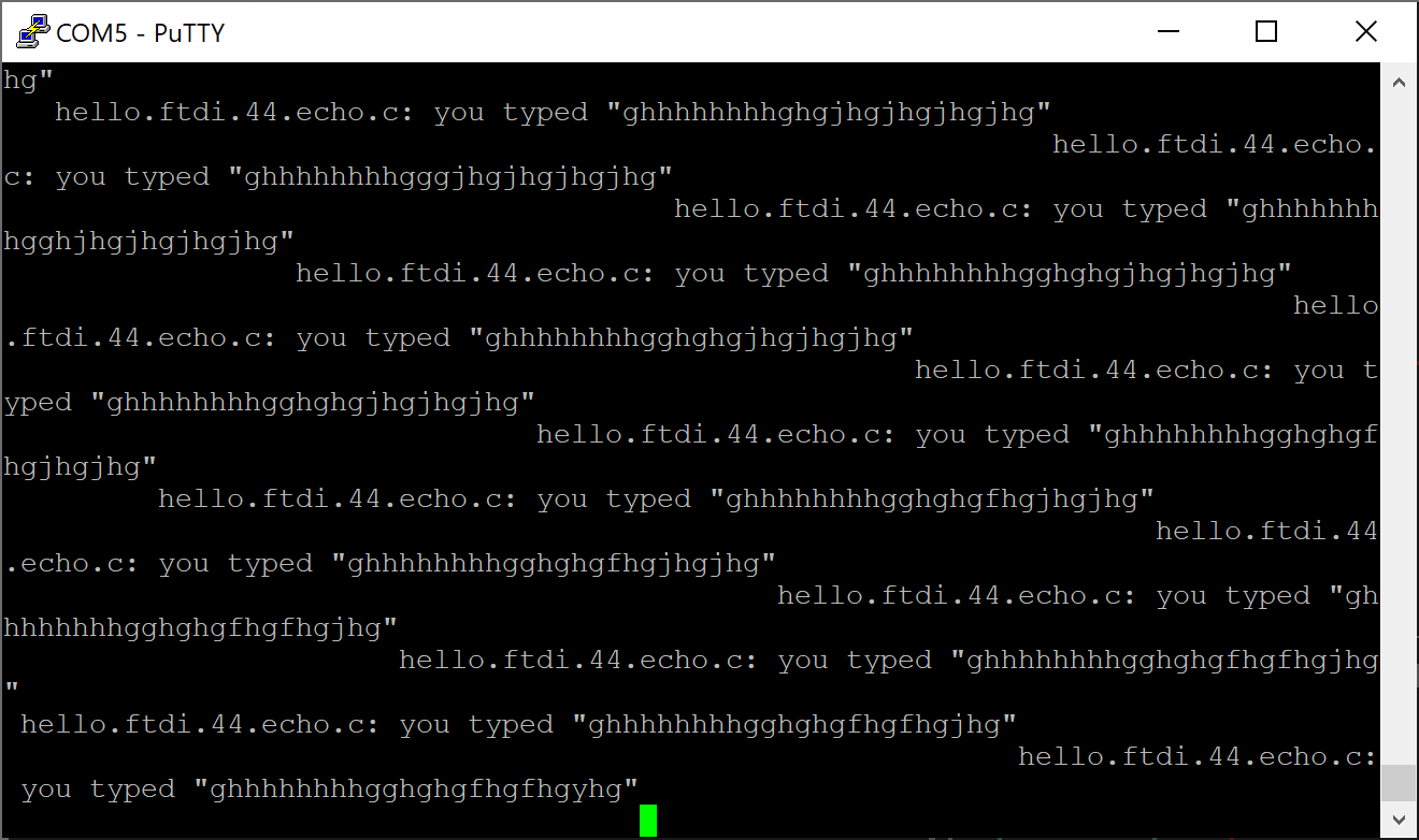
We decided to "send" three letters: U,S and B. We should be able to "receive" them on oscilloscope in binary format. Frames are made in 8bit packages, which are encoding a number/symbol/letter. After each frame "0" or low state is send, I believe it is used as start bit. On oscilloscope the order of visualization is LSB (less significant bit first) first. Let's observe the results.
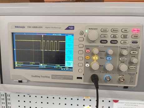
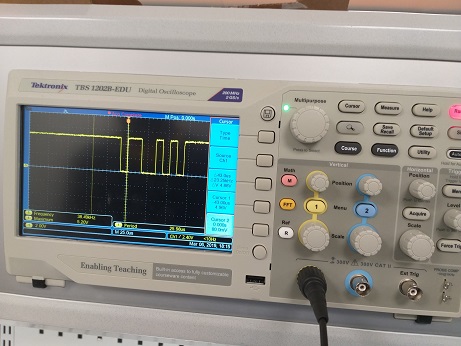
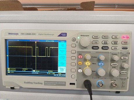
The baud rate was tested on the oscilloscope by measuring the time difference between number of bits. The oscilloscope reports the bit rate is at 11.49kbits/s. This is in the 5% tolerance of the used oscillator that manage the time that determines the baudrate. The baudrate was set to 115200 bits/s. This gives 115200/114900 = 2.6% offset from the theoretical bitrate.
That was nice and shown how microcontroller might communicate with external devices. There is also diode, which is blinking and so far unused button.
Individual Assignment
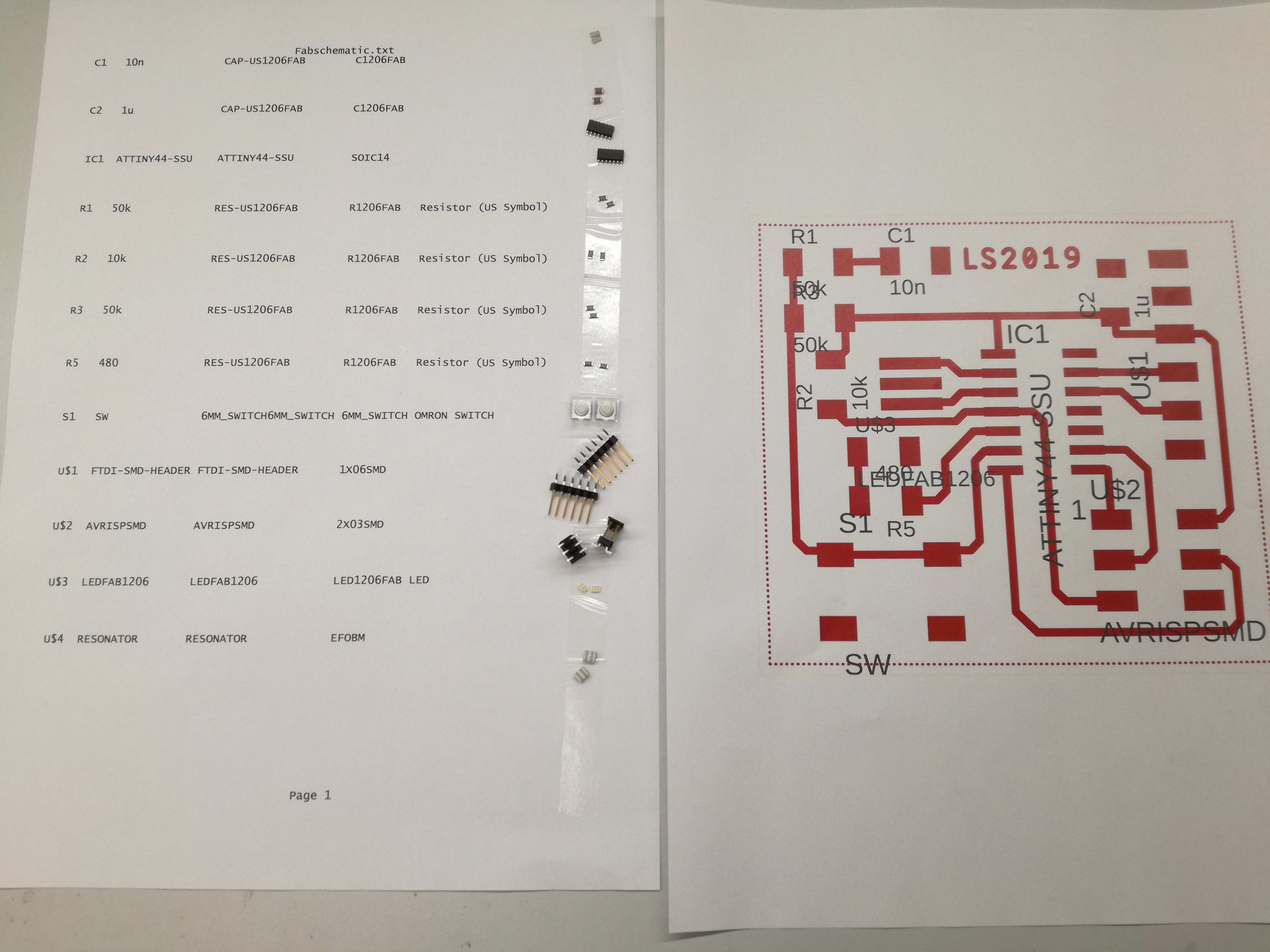
Schematic and PCB designing
The idea is to redraw the "echo hello-world board", which might be find here: Click!
Furtheremore, board should include following features:
- at least one button
- at least one LED with current limiting resistor
Following requirements are checking design rules, fabrication of the board, programming and testing it. Surprise, surprise. This is exactly what I did. I think music from The Last of the Mohicans will make it more epic.
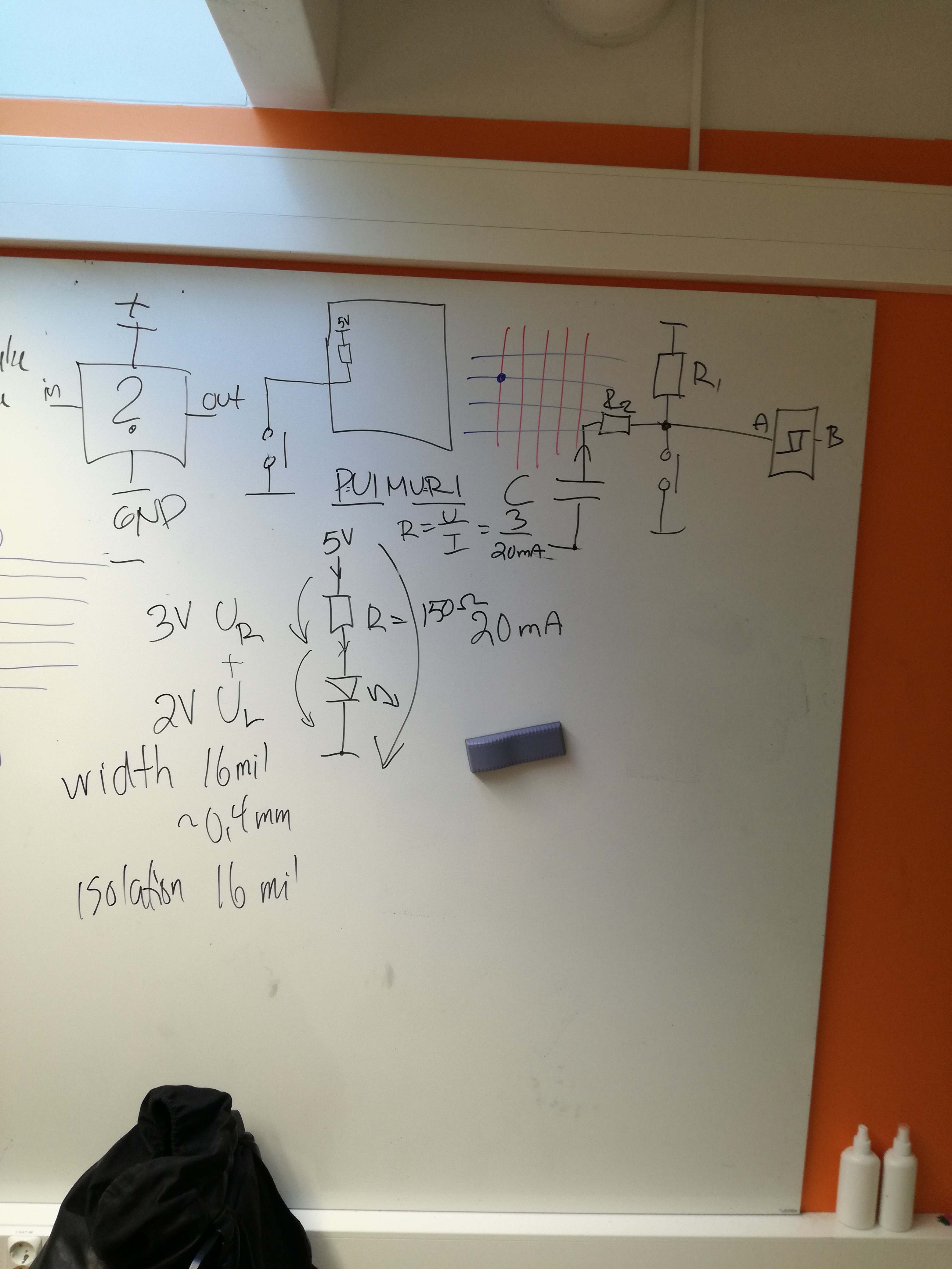
However, before we start. There is knowledge from the elders scrolls really handy. Photo can be found below.
In order to design the printed circuit board I decided to use Cadsoft Eagle . Ah right! It is currently part of Autodesk! So as most of my fellow students, I decided to use Autodesk Eagle, version 9.3.1. I believe it is Freeware, unless you are using more than two layers for wiring. There are of course other options for designing PCB such as:
- KiCad
- PADS logic
- OrCAD
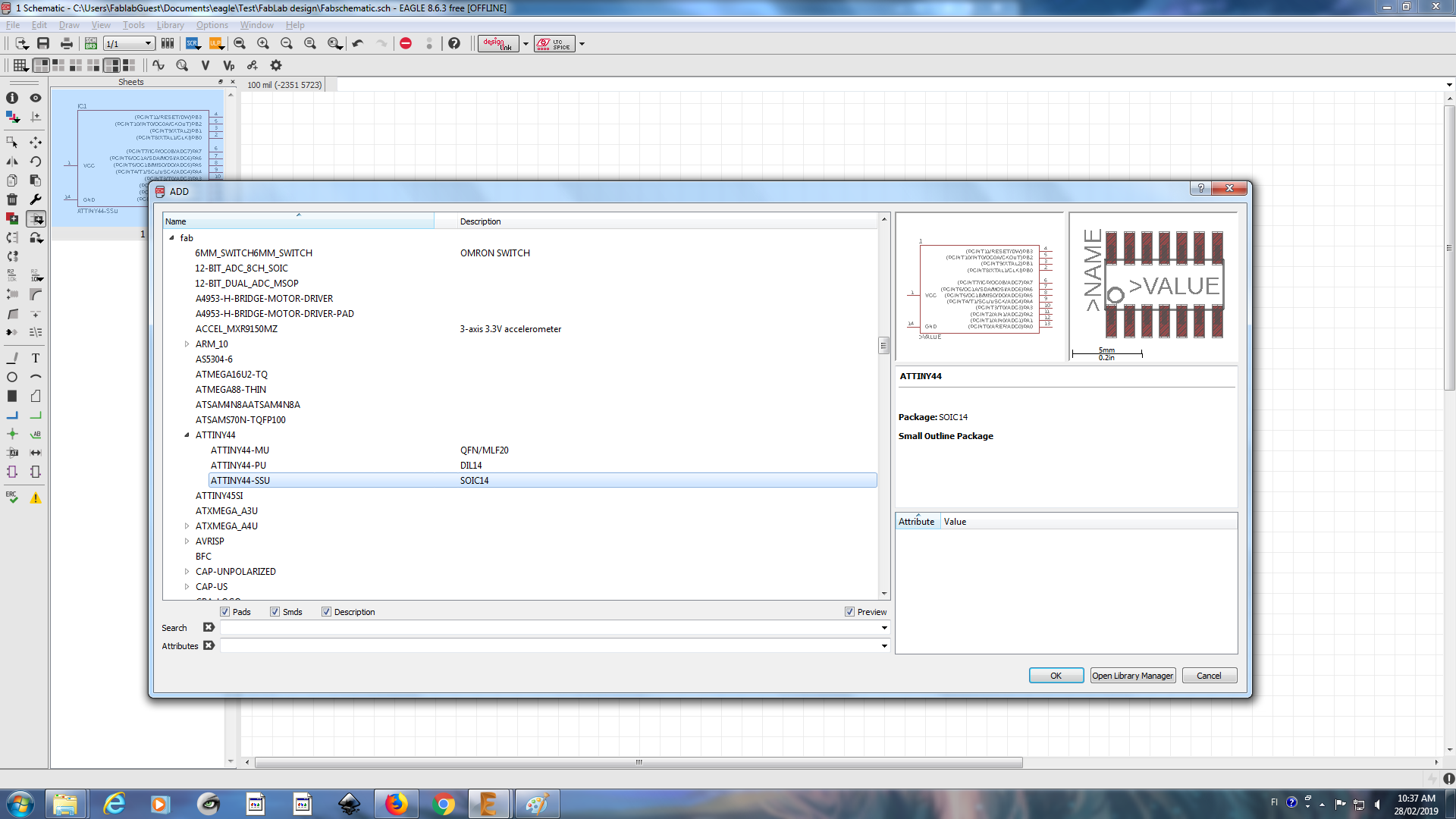
Nevertheless, I like what I know. I started from creating schematic. First step was to add library of footprints and parts to eagle. This was time saving step. I think Eagle has very good database of parts and their footprints. The issue is that usually knowledge of the exact names are required. As we are using components from different libraries we would need to scroll trough them.
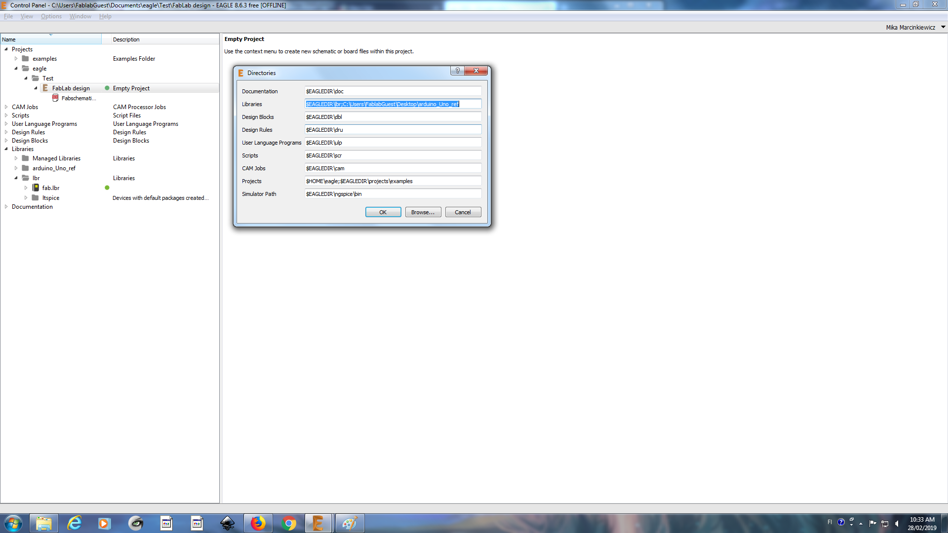
Next step was to create a project including schematic. Following step is adding parts to the schematic. Those can be taken from freshly added library. I forgot to mention that "Fablib" is standardized in a way that includes all the components available in every Fablabs around the world.
Placing the parts is crucial. Schematic should be easily understandable for future debugging and testing. What I really dislike is the way Attiny was sketched. All pins on one side. It forces putting "all the weight" of the schematic on one side. In future it will became more obvious.
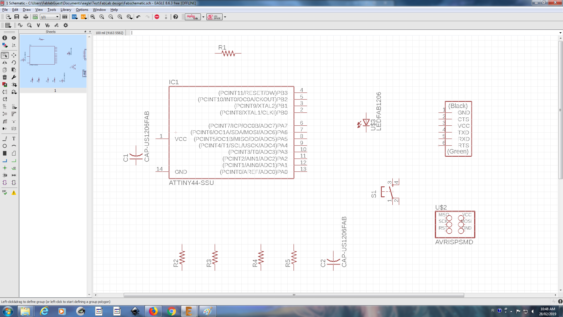
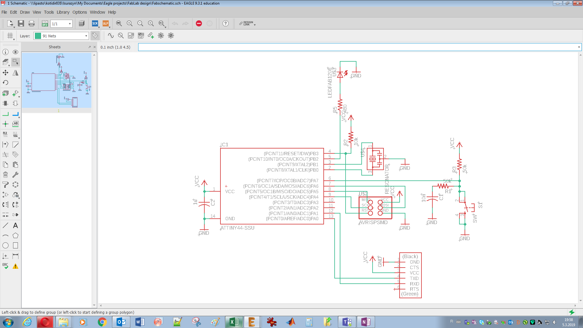
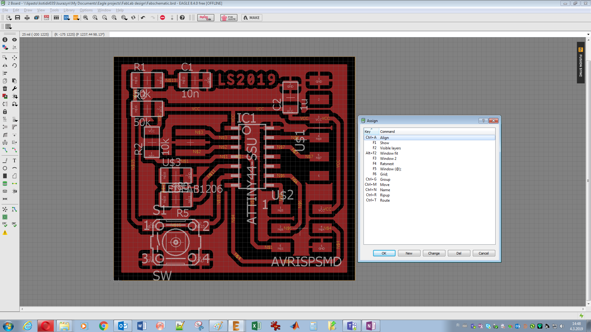
I really like shortcuts. Those can be assigned in Options/Assign. It is extremely handy when you design more than one PCB and must when you are working as PCB designer. If you are not using shortcuts - you are forced to use menu buttons on the left side. This is not rocket science, e.g. Move - moves component, Delete - removes component, etc. In order to connect components you need to use Wire and to connect nodes Jumpers are necessary. Using all of those features it is possible to finish schematic.
Now the fun begins. By pressing Generate/Switch to board PCB layout is getting created or edited. Components should be aligned and positioned in most efficient way, in terms of space and length of wires. Once again shortcuts are really handy. This time connection between points are made with Route tool. There are couple tips that might be important. Layout create menu is visible below. Just in front of tips.
- Ground can "poured" by creating polygon and naming it
GND
- Display is command to visualize or hide layers (Display none, Display top)
- Ratsnest should be used often
- Letters should be vectors
- Jumpers might be made by using 0 Ohm resistors
- Patience is the key
- Even more important is knowledge about schematic and connections between components
- It is not possible to delete parts, which has at least one wire connected to it
- All above are facts, not opinions
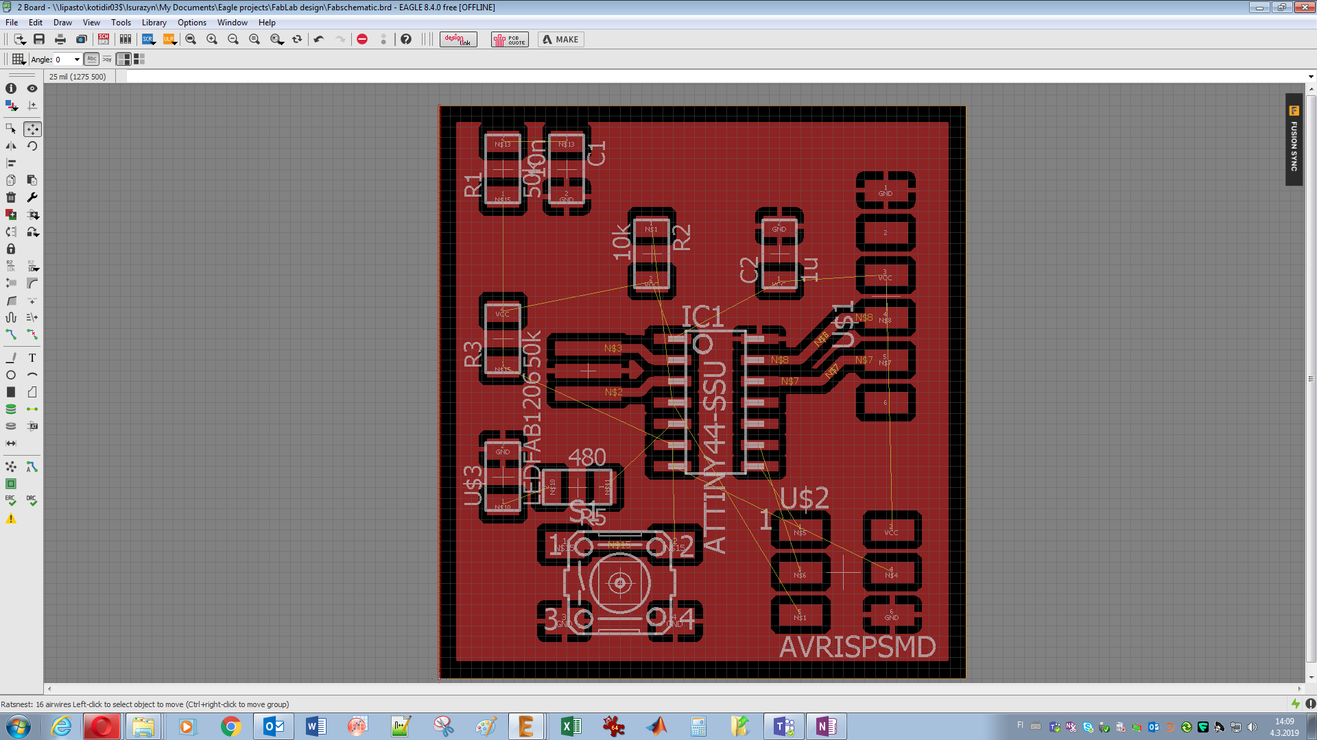
I decided that my clearance will be higher than standard - 16 mils. It is easier to fabricate and solder it after but it requires more careful placement of the components. Those can be find under DRC, which stands for design rules check.
At the moment we are in design rules. Just after placing components and connecting them I managed to have only single issue with the letters I put to customize my board. The width was too small. Nevertheless, I approved this Error as I knew it will be possible to mill it. Final board with some key shortcuts below.
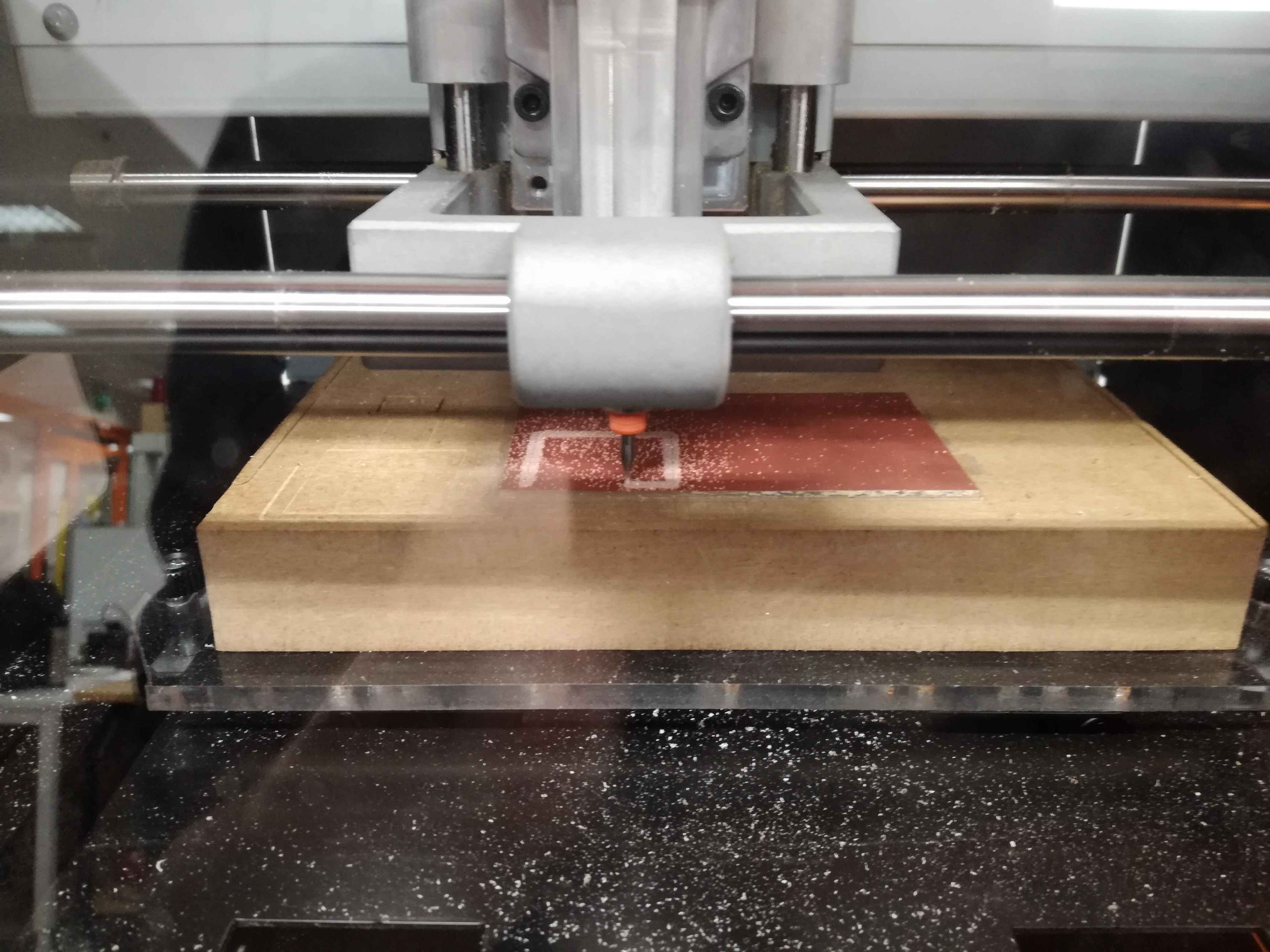
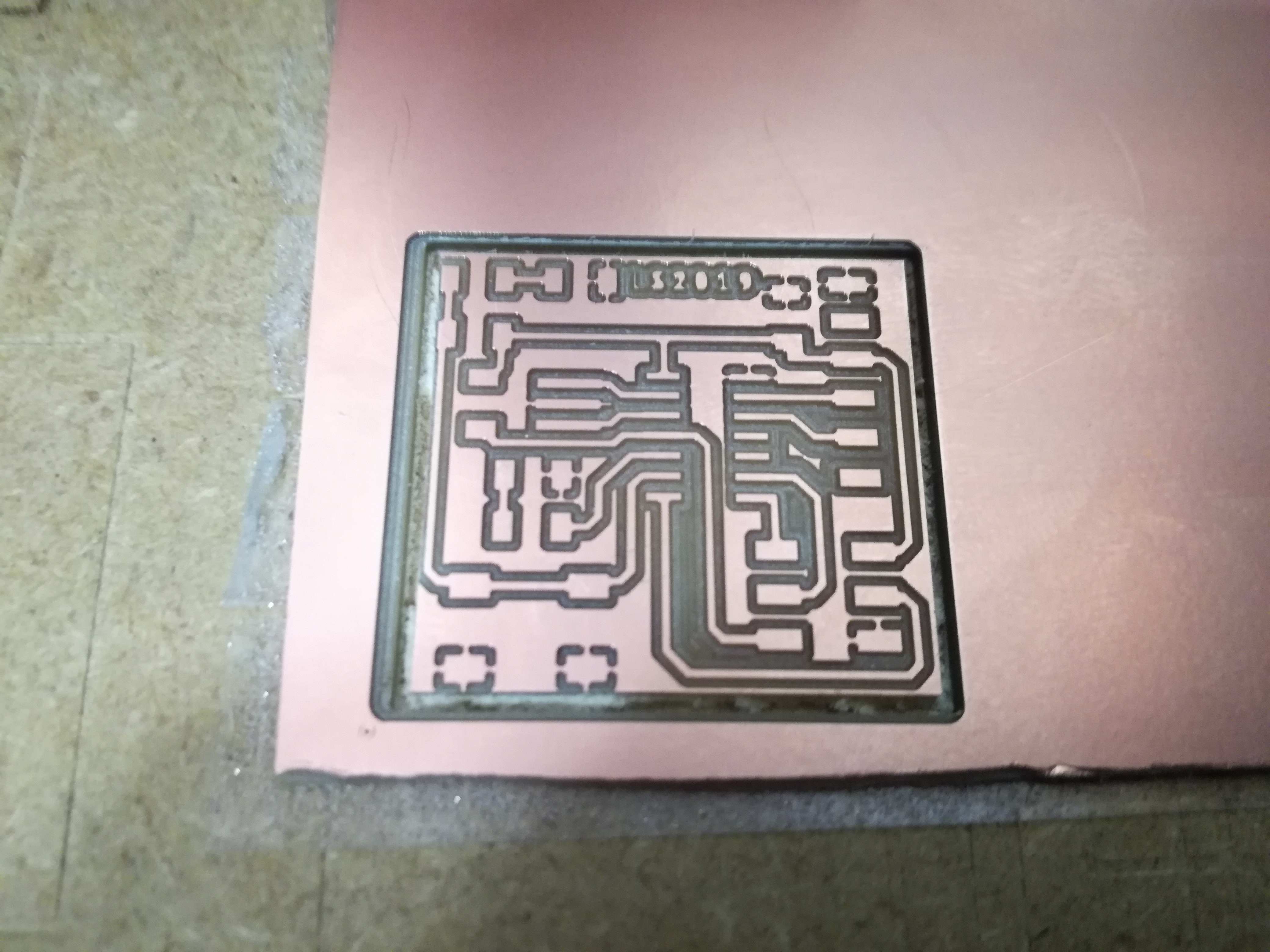
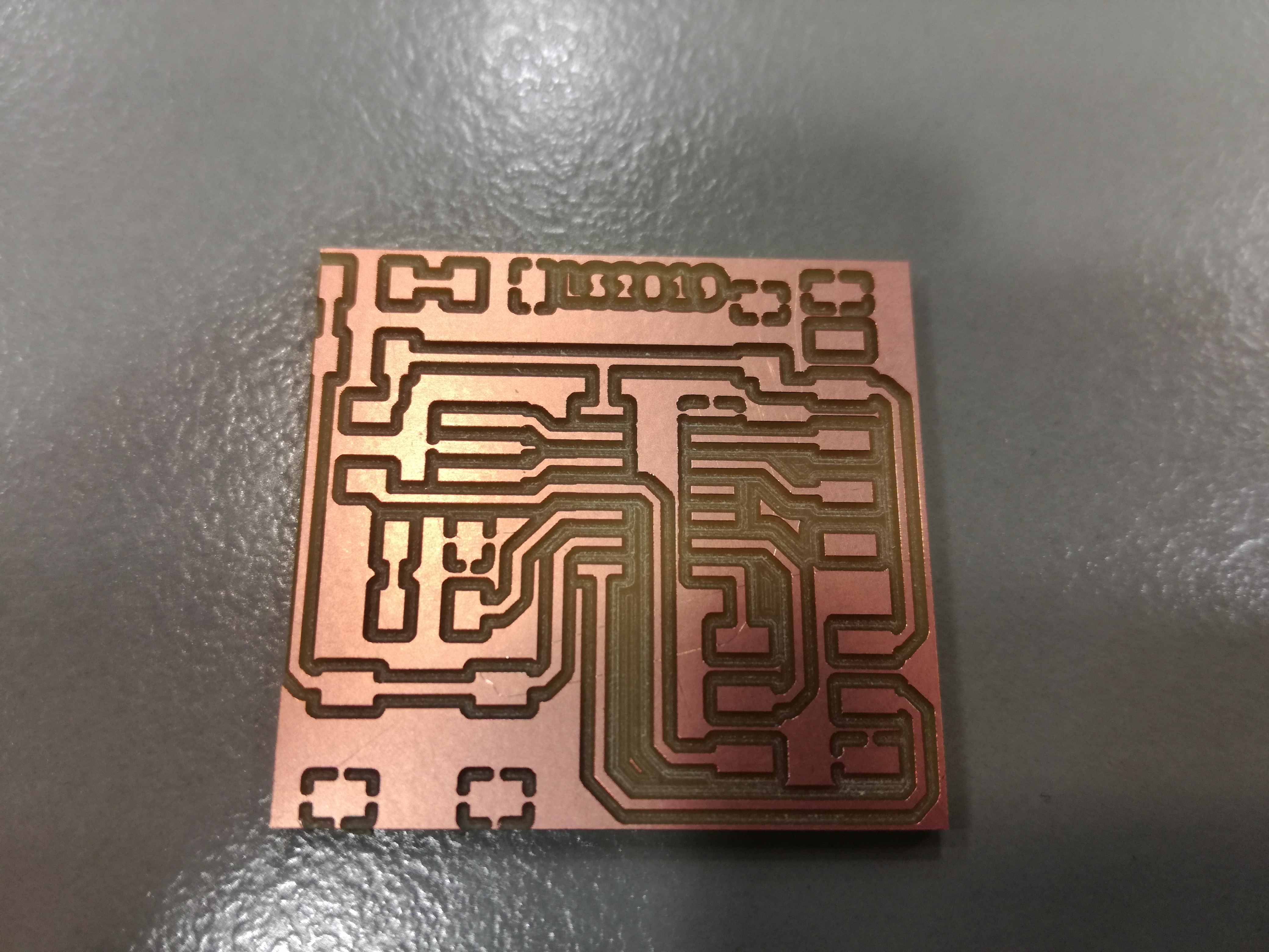
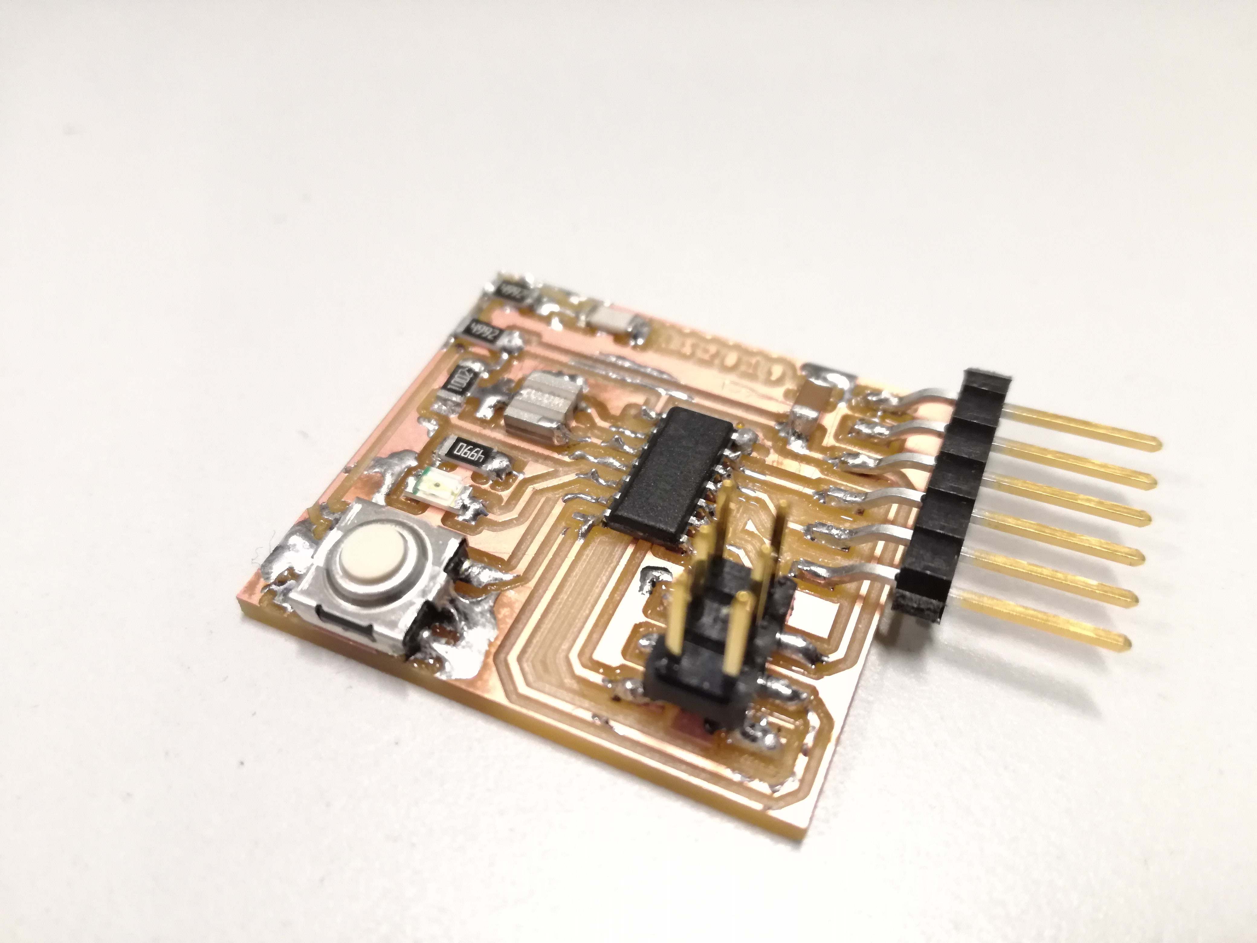
Milling and soldering the board
Using the knowledge and skills gained in previous weeks during Electronics Production Assignment (EPA) I managed to mill the board. All the steps might be find in mentioned assignment page. Some documentation during the process
Programming the board
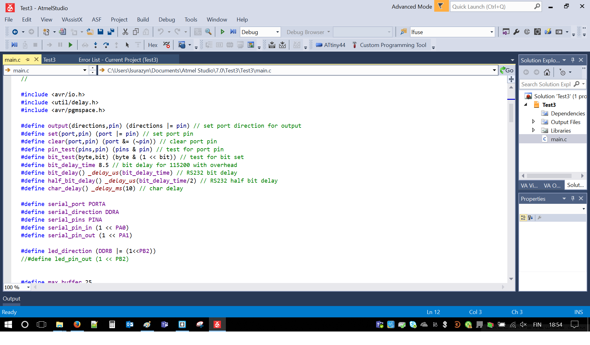
For programming purposes I decided to use Atmel Studio. I simply downloaded it from Atmel Website. Installation was fairly simple and it turned out successful. I decided that I will use Neil's code, which I took from Here .
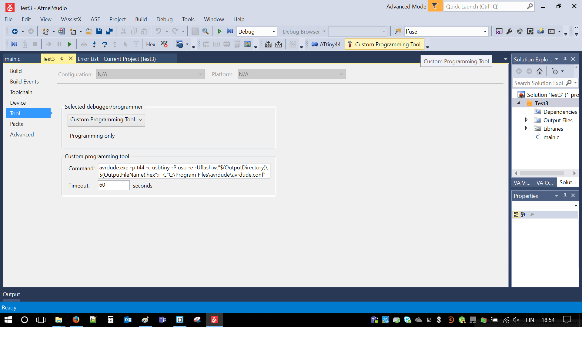
Before programming the chip, Atmel Studio required a bit of care. I little customization. I needed to add USBTiny and set it as legit programmer. With Tools/External Tools I added AVRDude path and named it USBTINY44.
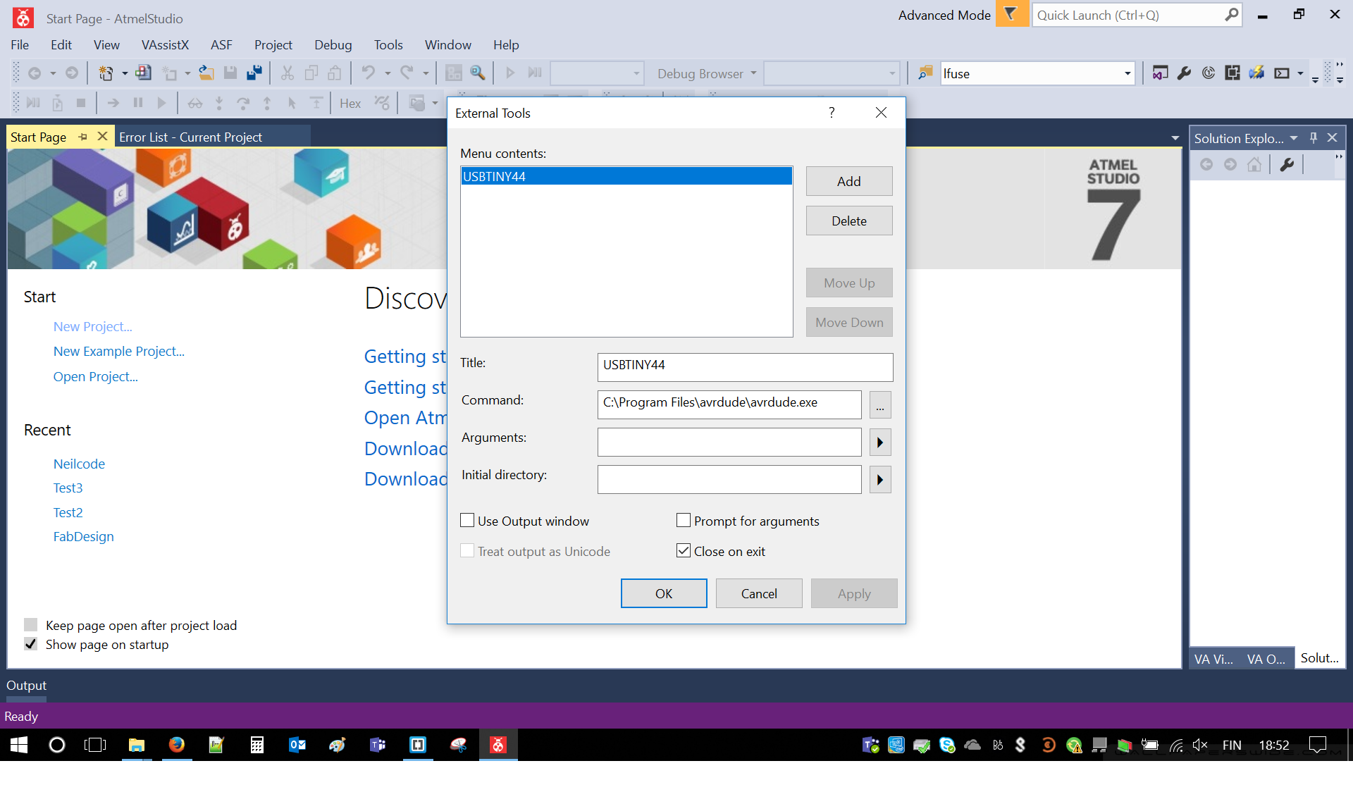
Then by clicking on Custom Programming Tools I added following command:
avrdude.exe -p t44 -c usbtiny -P usb -e -Uflash:w:"$(OutputDirectory)\$(OutputFileName).hex":i -C"C:\Program Files\avrdude\avrdude.conf"
It set all the variables for future programming, such as directories, configuration files, paths and usage of proper microcontroller for programming. Code is similar to previous Assignment - Electronics Production.
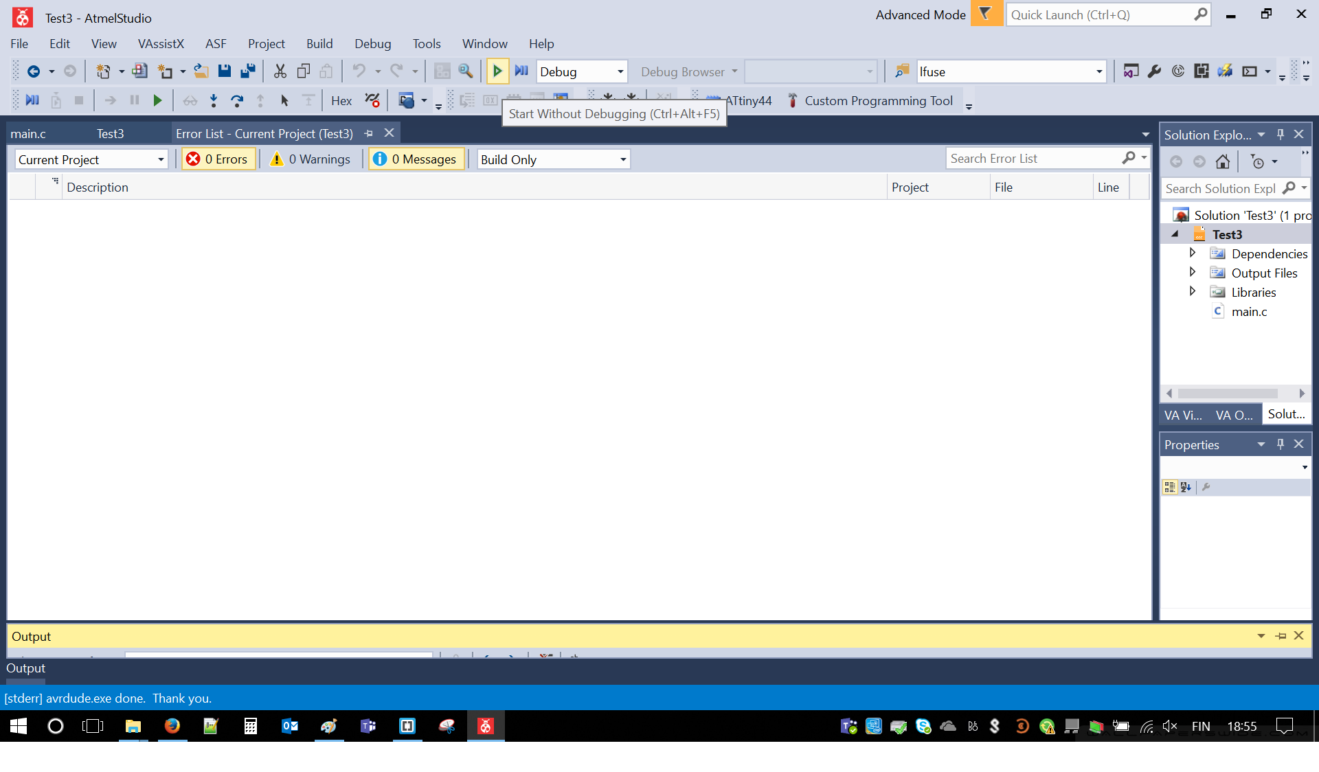
At this point I could program my chip, which of course I did. I had to click Start without debugging - as I don't have any debuggers. I was happy with clear output window. I guess I was lucky because it went without Errors or Warnings. Nevertheless it proven my Atmel Studio is properly prepared for future work.
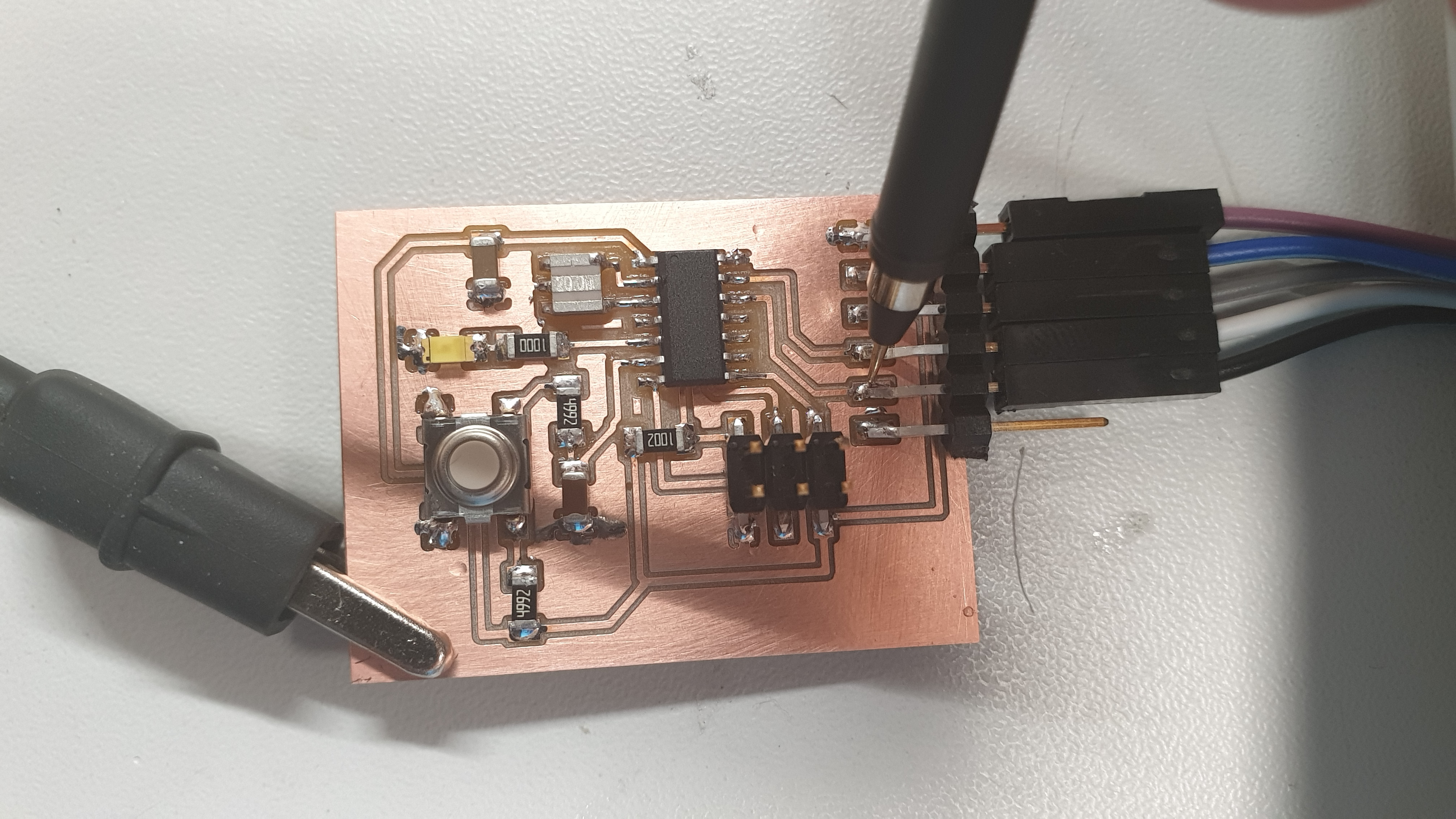
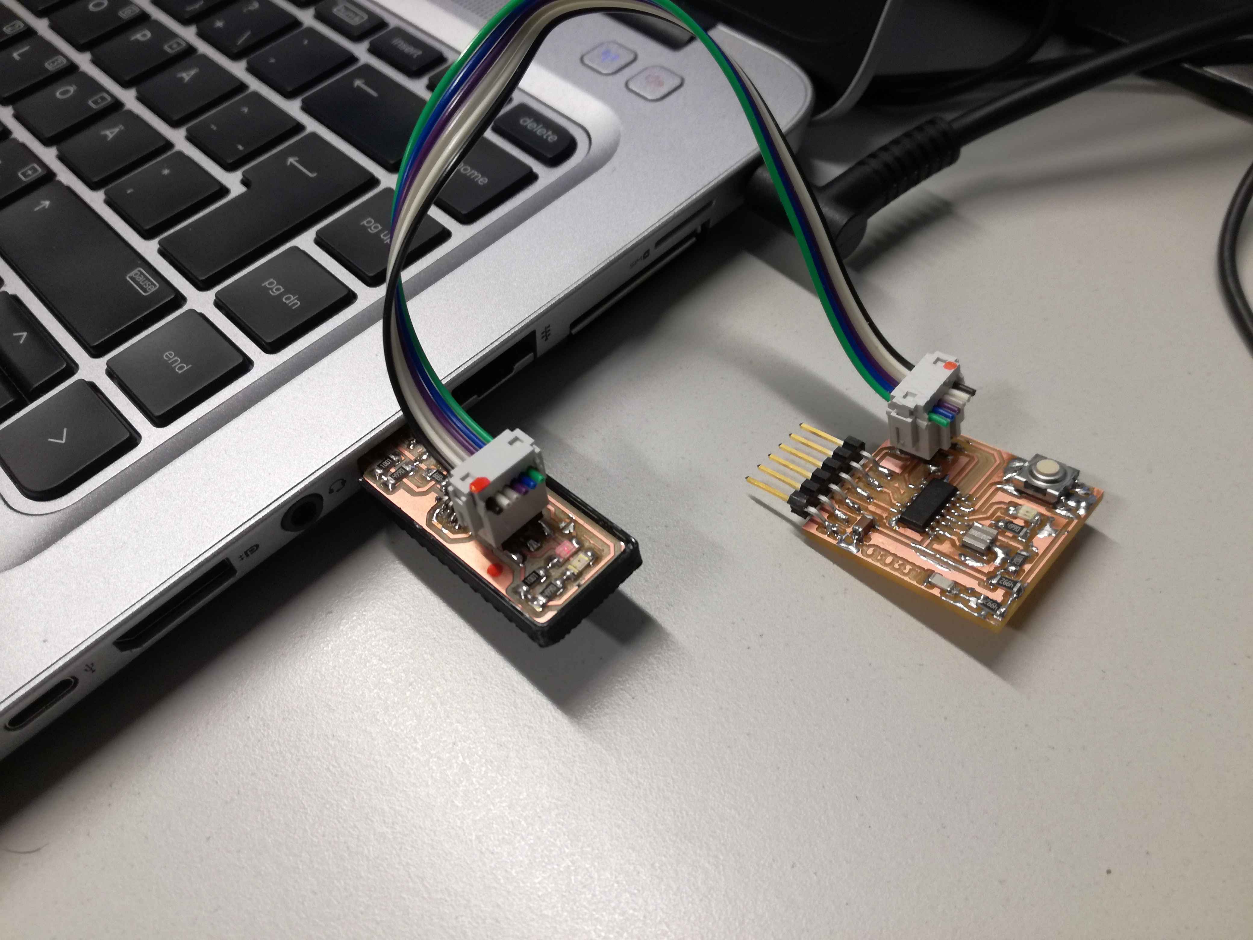
Below figure is showing connection between programmer and ISP connector of new board.
Testing the board
Testing was very simple. I had to connect FTDI to USB adapter (Future Technology Devices International) cable. Name is nice but cable is just adapter between USB and 6 gold pins. Immediately, after connecting the cable red LED started to blink with intervals. It proven that process was successful.
Files:
Download: Eagle project fileDownload: Schematic
Download: PCB layout
Download: RML Outline
Download: RML PCB