Final project: tangible 3d modelling interface
As I mentioned two weeks ago, my final project is an tangible 3D modelling tool which is a bunch cubes so user can make shape by assembling cubes like playing building block then the shape can be exported to PC as 3D model.
Casing
Since cubes will be assmbled into shape, size of one cube shouldn't be so big. I mesured size of chip (ATmega88) and dicided to make it 6cm on each side.
Also the magnet connector developed in machanical-design week should be integrated into each faces of the cube so cubes can easilly connect each other. The Design of the case is made by Rhino and it's supposed to be made of trasparent Acryl plate.
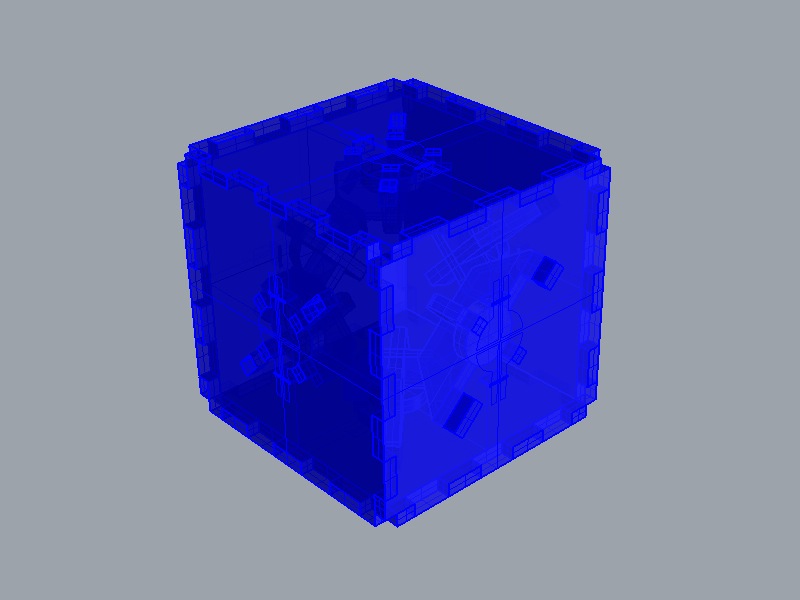
The cube has 3 male connector and 3 female connector. The Male connector always fit with the female connector in same direction. If cube is rotated to connect by other combination of male and female, positions of male/female connector still keep same position so it is easy to calculate coordinations of cubes.
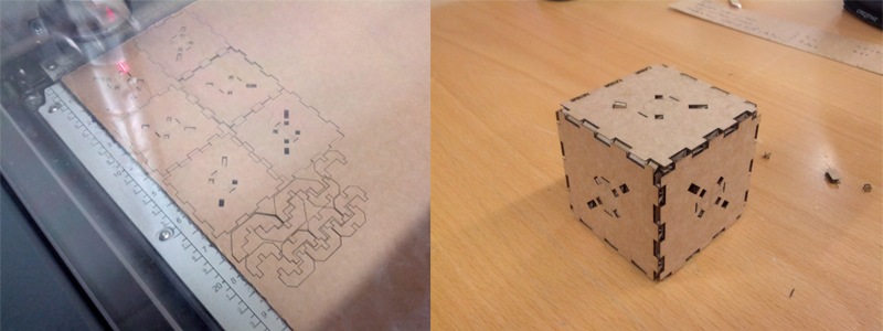
After generate cutsheets by Rhino Make2D commands, I cutted parts from cardboard jusu for checking structure correct or not.
Layout circuit
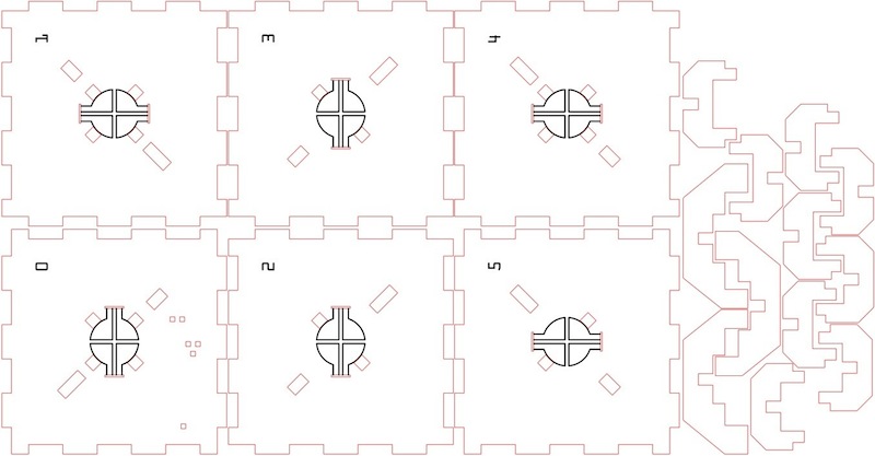
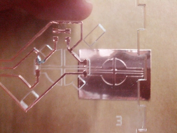
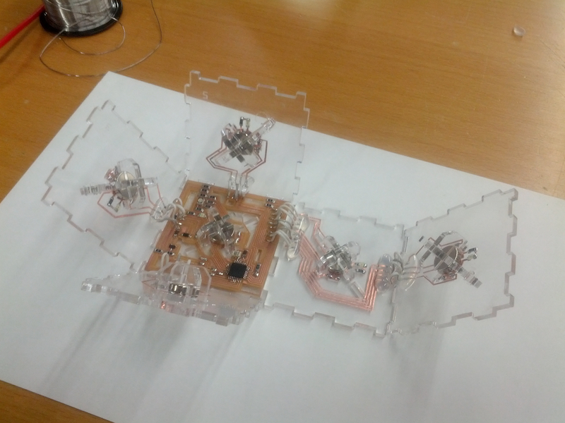
In the beginning, I planned to make circuit embedded inside cube by cutting copper tape. So It's possible to see light of LED embedded inside even case covered with circuit. I placed cut sheet of Acryil plate which is generated by Rhino as development view of cube and then designed layout of the circuit on it with Eagle. Here is blue print.
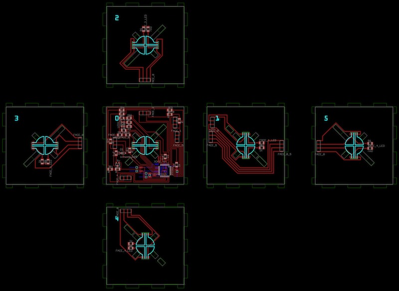
Green Lines are for cutting Acryl plates and blue part for engrave. Other parts are from Eagle lay out. To make it easy to understand sturucture of cube I numberd each face from FACE0 to FACE6. Circuits need to avoid case structure so it was required to check position of parts from Rhino and input it to Eagle.
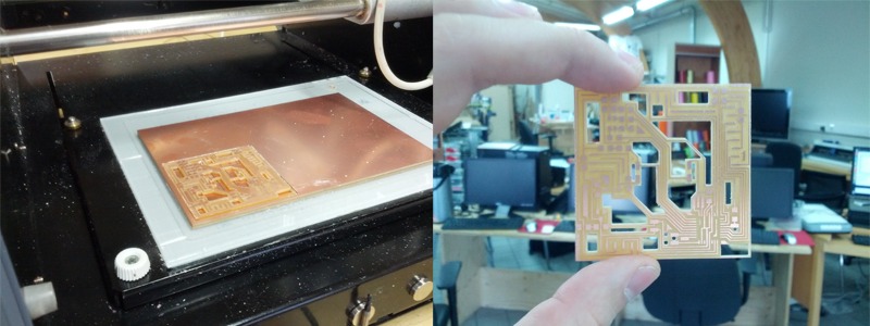
Cutting Acryl and copper tape
By using the cutsheet above, I laser-cutted traceparent Acrylic plates to make parts. It went well but problem was copper tape cutting.
I tried to make Circuit for FACE0 which has most narrow route around ATmega88 with Vinyl cutter but the machine rip off copper tape from base sheet in the middle of process so traces lose position and I had to stop the machine, change settings and re-start again and again. Since if Vinyl cutter cut throuh copper tape, it strated ripping off from sheet, I also tried to make pressuer of cutter lower so it just draw lines on copper tape and after "drawing circuit", cut it out by knife and hand. but as you can predict easilly it was so hard to remove extra copper tape. After struggling half day, I gave up to make it by cutting vinyl cutter and the plan is changed.
So I made circuit for FACE0 by milling with modela and cut out rest of circuits from copper tape by vinyl cutter. Still I wanted to make the cube as transparent as I can, I made holes on PCB board of FACE0 as many as possible.
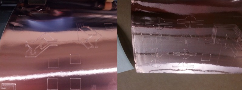
Cutting copper tape was fun if I know good setting and wide enough route of circuit. It was forst time to make circuit by cutting copper tape with modela and Fabmodules. Following instruction by Nadia Peek, I did some test cut to find good settings. Here is settings I used for cutting copper tape with Vinyl cutter in fablab Vestmannayjar.
- Force : 40
- Speed : 2.5cm/s
It still didn't cut out at some parts but It was cutted by hand easilly.(it was much easier than FACE0's circuit.)
And I found PEN FORCE slider Roland GX-24 has is very efficient so you can controll force of cutter easily in realtime.
Place copper tape on Acryl
Cutting is done so it's time to combine them. First I placed copper tape parts on FACE0 acryl part because FACE0 has two copper parts for connector and ISP of ATmega 88. Other FACE have only connector for communicating with other cube but only FACE0 also has ISP pad to program the chip inside since ATmega88 is placed on FACE0.
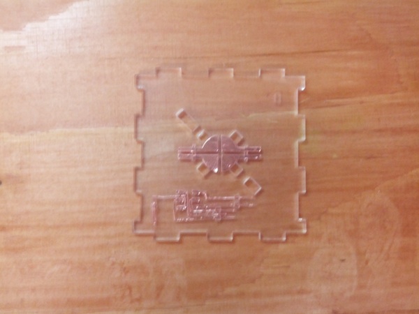
Legs of connector and ISP pad come to the circuit onside the cube through hole cutted by laser cutter to make it programable even when case is glued and chip is lock down inside the cube. After gluing PCB on FACE0, I put these legs to inside from outside with tweezer and then soldered legs with PCB inside so they are connected.
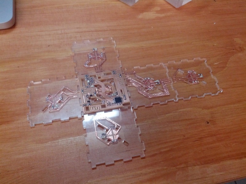
In the same way as above, rest of circuit were placed on other FACEs. There are marker engraved by laser cutter so it' easy to put connector pads on Acryl plates. And location of copper tape circuit can be realized by position of holes for legs of connector pads.
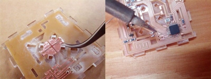
Soldering and assembling plates
As next step, I placed parts as development view of a cube like blue print showed in beginning of this page and soldered electric components on it.
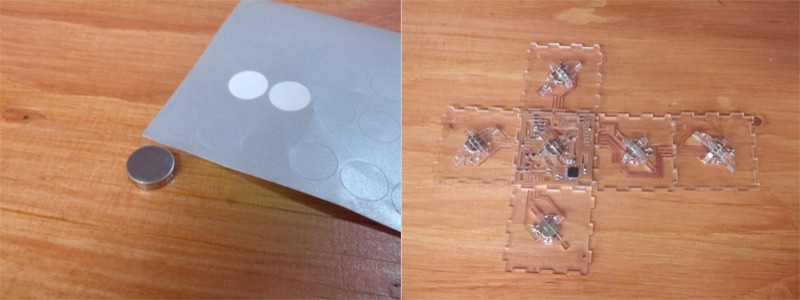
Before fixing magnets with Acrylic parts, all magnets were covered with vinyl which is cutted circle as same size of the magnet. Because surface of magnets is conductive, Vinyl is needed to avoid that circuit is shorted at some part by magnets. Then each plate were combined with magnets. Polality of female connector should be different from male connector to attaract each other.
I cutted white wire to make 24 of 2cm wire and fixed plates with masking tape not to move them from position. Soldered wires between FACEs to connect circuits embedded on each parts.
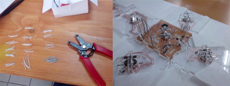
Before folding it into cube, I used glue gun to places wires were soldered because some parts rip off from acryl when I tried to fold it.
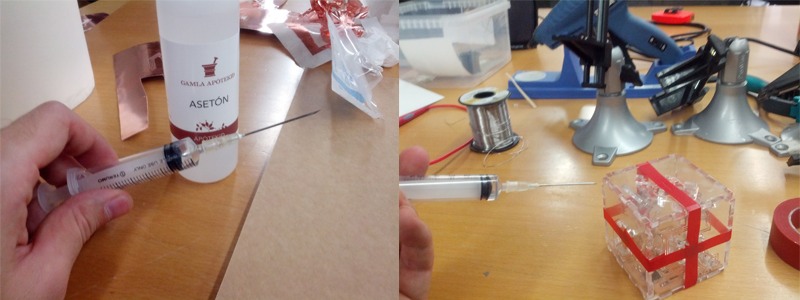
Glueing with Acetone
I've found a nice documentation about making acrylic box with Acetone. Acetone is not glue but it melt Acryl and dry fast so it can join acryl pieces by inserting between them. I used this trick to joine FACEs together into cube after folding. I bought an jnjector and bottle of Acetone at drag store. Then I fixed plates as cube with tape tightly and put drops of Acetone on edges of the cube by using injector. Leaving it for 2,3 hours, plates are completely stick together.
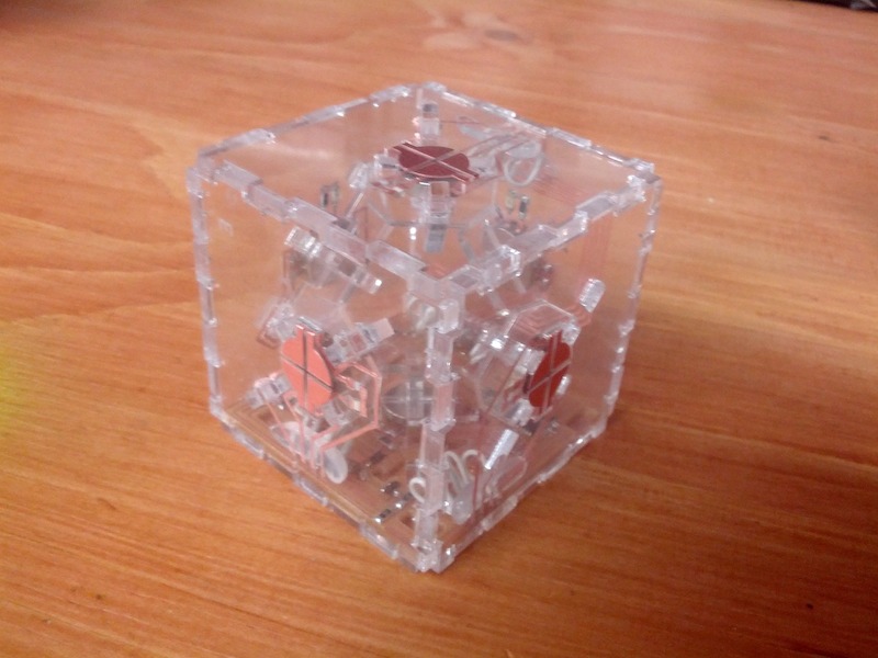
Removing tape after Acetone dry out, Here is the cube. finally physical part is done. From next chapter coding part is started to give some intelligence to it.
Makefile
To write program into chip inside cube, I made Makefile based on Neil's Makefile of APA network. I used different chip for the board so I needed to modify it from ATtiny44 to ATmega88. I typed "avrdude" in Terminal and its description explained which options it has and how these options works. To make Makefile, I checked options listed up below.
- -p : Required. Specify AVR device. m88(ATmega88), t44(ATtiny44)
- -c : Specify programmer type. usbtiny(FabISP)
- -P : Specify connection port. usb(USB port)
- -U : Memory operation specification.Multiple -U options are allowed, each request is performed in the order specified.
And fuse code generated by Fuse calculator is...
-U lfuse:w:0x5e:m -U hfuse:w:0xdf:m -U efuse:w:0xf9:mSo, lines for fuse ATmega88 in Makefile is...
program-usbtiny-fuses: $(PROJECT).hex
avrdude -p m88 -P usb -c usbtiny -U lfuse:w:0x5e:m -U hfuse:w:0xdf:m -U efuse:w:0xf9:m
After doing fuse, Writing program with these lines...
program-usbtiny: $(PROJECT).hex
    avrdude -p m88 -P usb -c usbtiny -U flash:w:$(PROJECT).hex
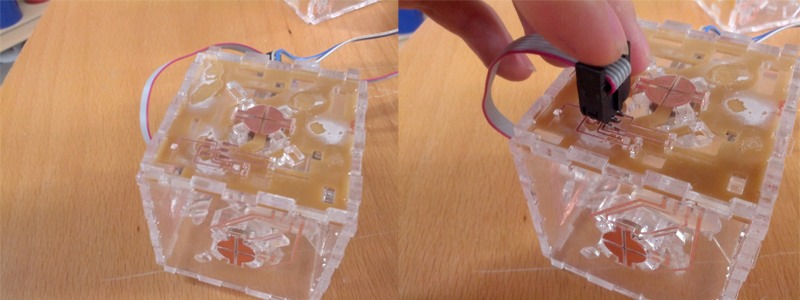
I put 2x3 pin header to socket of FabISP and press it against to ISP pad on FACE0 of the cube. While do that type command to fuse the chip. If hold ISP pin correctly, fuse will be done.
Blinking test
Just for checking the cube programmable or not, I wrote simple test code which makes LED embedded inside blinking. And the cube can shere the power if it is connected with another one connecting with battery. Here is how it works...
Coding C for the chip
Based on APA network sample, I wrote C code for ATmega88.
I listed up which pins are used as IN/OUT for each faces.
- FACE0 - IN:PB0, OUT:PD7
- FACE1 - IN:PC5, OUT:PC4
- FACE2 - IN:PD0, OUT:PD1
- FACE3 - IN:PB2, OUT:PB1
- FACE4 - IN:PC0, OUT:PC1
- FACE5 - IN:PC2, OUT:PC3
- RED: PD6
- GREEN: PD3
- BLUE: PD5
As starting point, I deleted unnecessary functions for my project from sample code. For example, original sample code has 2 reading A/D pins input function but the cube doesn't has such a A/D input device inside so I just deleted it to make the code slim.
After the diet, IO ports for APA communication are expanded for 3 ports to 6 ports. To define the APA IO port, I should write down these lines in the code.
- port_X.pins_in: name of pins IN pin belongs to
- port_X.port_out: name of pins port OUT pin belongs to
- port_X.direction_out: direction of ports OUT pin belongs to
- port_X.pin_in: name of IN pin with shifting 1 like (1 << PA4)
- port_X.pin_out: name of OUT pin with shift 1 like (1 << PA6);
- port_X.path_in_length: initialize length of packet it receives.
- port_X.path_out_length: initialize length of packet it sends.
- port_X.id = id for this port
- port_X.next_port: name of next port
By Original source code of APA network, it's possibrle to know only out-bound path to the destination node. To know also in-bound path, I add new command to source code as I did in interface week. It's needed to figure out coordinations of cubes in next chapter.
I tried APA sample program of networking class by connecting cube with PC through APA FTDI board I made in network week and it works as it is. Now I need to develop software runnning on PC.
Scanning coordinations of cubes
I wrote interface software with Python and I used wxPython as widget and PyOpenGL for generating 3D model. As starting point of making interface software, I just tried to figure out where are cubes located from path of APA network and geometry of Cube.
By using new command I mentiond above, now it's possible to know in-bound and also out-bound to path to cube. It enable to culculate cube's coordination from path and origin cube which is located (0,0,0). So I made function which can figure out coordination of cube by input path it from origin cube and position of origin cube (which FACE is directed as X,Y and Z.). It's basic function so display just showed numbers but it recognized coordination of cubes correctly. Here is video...
3D model from Cubes
For 3D model part of software, I wrote code based on example code I found in this page. In the software origin cube which is cube located on (0,0,0) is colored as red and other cubes colored as blue. Unfortunatelly, I had only two cubes at that moment so display shows one red cube and one blue cube maximum but if user changed comibination cubes, 3D model also change it own shape related to physical cubes. After scanning, 3D model pop up on display and user ca rotate it by dragging mouse.

For next step
- I've found a problem when software scannning geometry of cubes by APA networking. Sometimes communication got stuck between nodes. it looks like some node keep sending packet even when thier job is canceled by timeout. To solve this, Probably checking APA library form basic is required.
New design of connector is absolutely needed since latest version often had bad connection. I'm thinking about using tiny springs so spring fill the gap between male and female connector.
It is not enough to publish as opensource hardware. I need more time to make it. But when it become worth enough to share with others, I'll make it open-design definitely.Moreovere my ideal plan is case of littleBits so the design is open for everyone but they can also order kits.
Bill Of Material
Here is material list and price I used per cube.
- Transparent acrilyc plate (3mm thickness) _ 150 squar cm _ $1.1
- 3M #1126 copper tape _ 150 squar cm _ $0.7
- ATmega88/328 _ x1 _ $1.3 ~ $2
- MAGNET 1/2inch diameter _ x6 _ $5.4
In total, one cube cost around $8.5
Extra cost for tools
- injector _ $0.4
- Acetone 100ml _ $9
Resource
- Grid Cube : this ZIP file contains Eagle file, cutsheet of Acryl+copper tape, and C code and Makefile to make GridCube.
- FTDI board : this ZIP file contains Eagle file, C code and Makefile to make FTDI board which I used as bridge between GridCube and PC.
- Python Script for Grid Cube : this code is for visualization by using PyOpenGL. It's same software intoroduced in last video in this page.