Electronics Design:
We started out by diving into Eagle. At first that seems incredibly imposing, with the massive amount of libraries available. Luckily the Fab Library (found here) is not as imposing and extensive as most others.
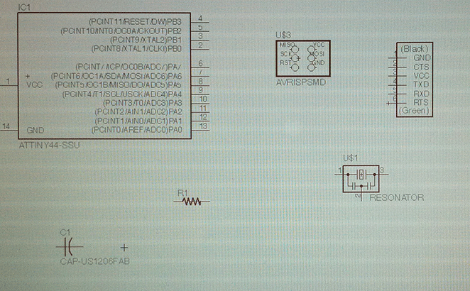
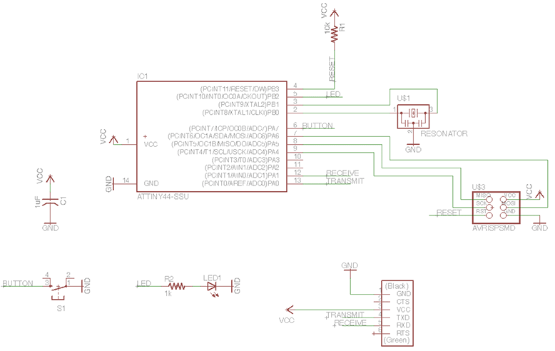
After adding the needed components for the original ISP board, my schematic looked a little like so:
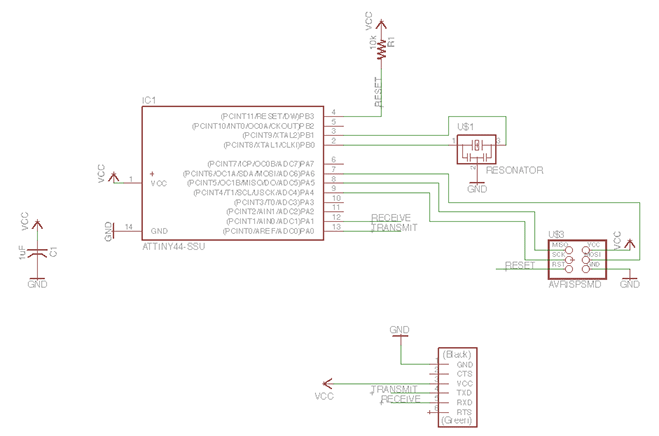
From there, we needed to still connect all these components together by drawing in the wires. Drawing in all the wires can become quite messy, so we quickly learned some shortcuts. By drawing only a part of the wire from a connector, and using a label to name it, and having another wire connected to a connector with the same name, Eagle will ask if you want to connect them together. This saves a lot of clutter on the screen. We also added an extra library to pull assets from, which included the ground (GND) and power supply (VCC) connections (this library is Supply1, which contains Supply Symbols).
After connecting everything, we end up with this:
I'd like to say that I fully understood what parts we were connecting together and why, but I still don't have a very clear grasp on it. Most of the layout design was done together with the coordinator Bas Withagen.
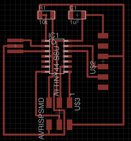
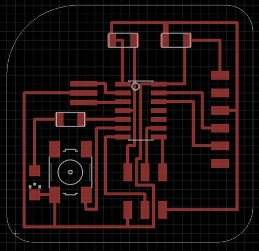
From here, we told Eagle to make a PCB out of this schematic. With the click of a button you go to the design screen and have a jumble of components that need to be carefully laid out. Eagle is pretty good at showing you what parts need to be connected to what parts (as per your schematic), but you still have to draw the physical lines in, to make sure there's no overlap and that they're not too close to another connector.
After laying it out, you can use the Design Rule Check (DRC) tool in Eagle to check if the gaps between connectors are physically spaced far enough. For this you do have to set the correct size of the milling bit you'll be using. Eagle will show you where there are spacing errors (if any) and you'll have to tweak them and run the tool again.
After some back and forth fiddling, we ended up with this layout of the PCB for the schematic.
But we're not done yet! This is only the design of the original PCB that was supplied, but we still need to modify it. As per the assignment, we need to add an LED and a switch into the mix. This meant adding three components. The switch, an LED and a resistor for the LED. We went back to the schematic and added these components. There were still plenty of spots free on the Tiny44 processor, so we chose two (which were on the same side, we double checked this in the board layout) and connected the wires. From there we again jump into the board layout and the added components were there. They still needed to be placed into the layout and connected though. Luckily, there was a perfect large area within the design on the left, so I ended up adding them there (though I did extend the open area a little to fit it all in). Here I also added the line around the board design, which will indicate how the modela will end up cutting out the board outline to seperate it from the plate. I decided to get a little fancy here and add some rounded edges to it.
Technically, I was ready to export the board and have the Modela mill it out for me. However, I saw two vast empty spaces staring back at me from the board layout. One on the top left, and one on the top right. Seeing that there were still a few connectors left on the right side of the Tiny44 chip, I decided to be daring and add another LED to the mix. In the schematic, I basically copied the component that consisted of a resistor and an LED and connected it with one of the free connectors on the Tiny44. I wasn't sure what to do with the open space at the top left, but I soon had an idea that you'll see if you read further on.
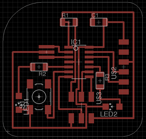
I named this board the Goodbye Double Plus. The first iteration was the Goodbye, since every other board seems to be 'hello' or 'hello world'. The second iteration was the Goodbye Plus LED or just Goodbye Plus. After I added the second LED, it became the Goodbye Double Plus.
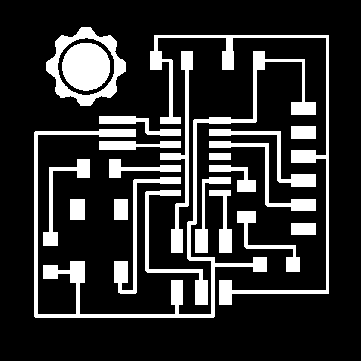
From Eagle, I exported the board as a monochrome image. In the settings you can set the DPI you'd like to save it as. This will give you a nice and clean .PNG file to work from. There's still an extra step before you're ready to send it off to the Modela, so I booted up Photoshop to create the interior and exterior images that I'd need. The exterior is just the outline of the board with the entire inside filled in with white. This we'll use to cut out the board so we can take it off the plate. The interior is the entire design sans outline, so the Modela can mill all the paths neatly. Since I was in Photoshop, I sneakily added a custom logo to the board, to add some personal flair to the board, so I could instantly recognize it in a crowd.
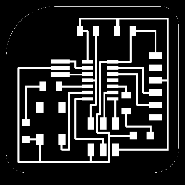
The board as it is exported from Eagle.
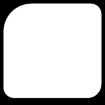
The Interior and Exterior files ready for the Modela.
From here it was a fairly straightforward process to get the board milled with the Modela. For a description on how I've previously used it you can go back to #4. Electronics Production.
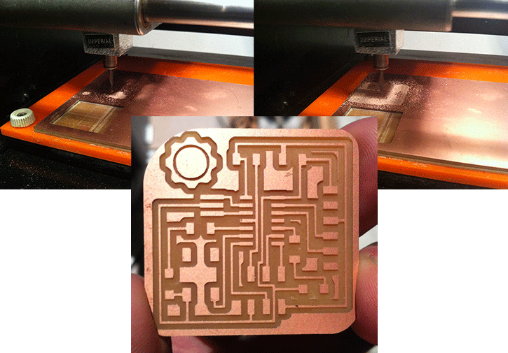
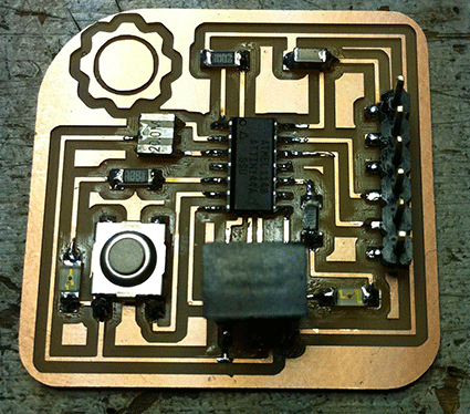
The last step here is of course to solder on all the components (correctly!) I gathered all the components together and started working diligently. I ended up adding one green and one red LED to the board, to spice things up a little for when we program it. Overall the soldering was fairly straightforward to do, and I didn't really run into any snags.
Here's the completed board, assignment 6 was a success!