This week we had to redraw an echo hello-world board and add at least a button and LED, make and test it.
As in week 04 I used KiCad to design my PCB. I look at the assignment of my instructor Lena Hagenauer and desinged a board arround the AtMega328p.
Here you can see the circuit diagramm and the final layout:


I then exported my design as gerber-files and imported it into the software of our circuit-board milling machine.
I quickly looked over the settings, inserted a new copper plate and started the job.
But everything went wrong...
As I said before our pcb-milling-machine is capable of automaticly switching between up to 12 milling bits. The LPKF tried to change to the first needed bit and jamed the tool head into the bit, breaking the bit-holder and spitting out some error messages...
You can see the bit not sitting as it should and the holder being bend:


I called one of my instructors, who is also the one in charge for repairing this machine and we tried to fix it via call, but it didn't work and I had to block the machine and mark it as defect.
A little bit frustrated I drove back home. While driving I thought about other ways of fullfilling this assignment in time and quickly remebered, that the Snapmaker 2.0 I have at home is capable of milling small things.
So when I arrieved home I started reading about how to use the Snapmaker as CNC-machine, as I had never used it before in this way.
I downloaded the corresponding Snapmaker-Luban software and looked for the bits that had come with the machine itself. The 1.5mm flatend-mill was a lot thicker than the 0.2mm bit that the lpkf would have used, but I hoped it would work.
I then exported my Kicad design as SVG-file and imported that into the Luban software. I tried everything the same as the tutorial I found had told me, but what ever I've done wrong, the software wouldn't do what I wanted it to do...
For some reason it always tried to cut out my tracec, instead of cutting around it:
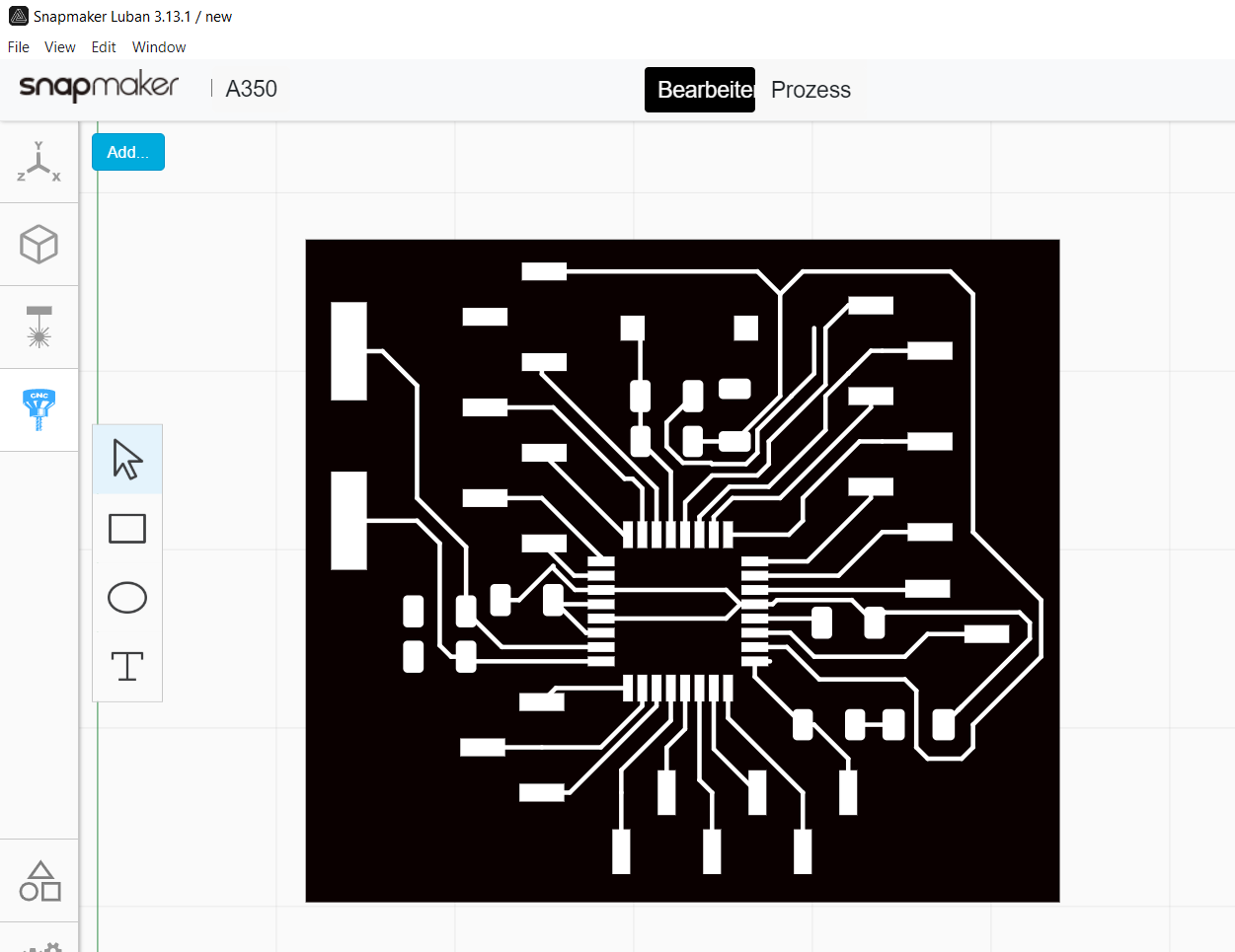

I tried reversing the color, I tried importing it as PNG instead of SVG, but it never came out as I wanted it...
More frustrated than before I gave up...
I had almost accepted the fact that I would not be able to finish the task until later when a very strange idea crossed my mind. As we talked about different materials for 3D printing last week we also talked about condictive materials.
And I luckily have a role of Proto-Pasta Conductive PLA here at home, so my strange idea was to 3D print the pcb and solder the components to it.
Yeah I know, it sounds absolute dumb, but I was so attached to this idea, that I started to work on it.
I converted the exported SVG from KiCad to a PNG and imported this into Fusion 360.

I started to import all my components and set them where they would normaly be on my milled PCB:

I then started to redraw the lines with a minimal thickness of 0.4 mm, because that the size of the nozzle of my 3D printer and I wanted it to be exactly one line thick. At some cases it was very difficult, but at the end I got all pads and traces redrawn:

At the end I extruded all traces with 0.4mm height, all pads with 1mm height and a base plate of 3mm:

After I imported the STL into Prusa Sclicer I changed my settings to a layer height of 0.1mm an a linewidht of 0.35mm. I added a color change at the point where the traces would start, so that I can change the white PLA to Proto-Pasta conductive PLA:

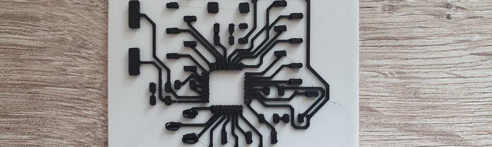
After 40 minutes I've got a printed PCB that looks quite good to be honest:

After a first look I found out, that the pads of the AtMega328p were all fused together. I wanted to quit againt but I realized, that I had a 0.2mm nozzle here and that I could print more prezise, if I change the nozzle.
So I changed it, changed the settings in the Prusa Sclicer again and started printing:

It's still not perfect and I havent been able to build my hello world board with it, but I like the idea of a 3D printed PCB and I will definitly work on that again!
As said before I waited till our PCD-milling-machine was fixed and I could work on it without a problem.
I recutted my design as in my first attempt, but this time it worked as it should!
I then used the same process as I did in Week 4 and soldered the components to my board.
While in the soldering oven the airmovement blow away some of my pin headers, which you will see in a moment.
Nevertheless I recieved a "good" looking board:

Note that those wires soldered directly to it are the SDA / SDC connection used for the I2C communication, which I need in an other assignment.
I used an arduino uno to programm the board. For that I used this Tutorial as a refference.
To confirm that my board worked as it should I wrote a quick blink-tutorial script which will let the internal LED of my board blink in 200 milliseconds interval:

Here you can see the board working as it should:
As group assignment we had to test an observe our circuit board.
The main tool we use to test our board is a normal multimeter. With this we can messaure the resistanz, check if connections are where they should be and or if there are connections that there shouldn't be.

For later testing we also got a picoscope in our lab, which is like an osscilloscope but you connect it via USB to the pc, but we haven't used it before and only need it in some special cases.
Our testing of the opereation of a microcontroller using a multimerter and a oscilloscope ist linked on the page of our groupmember Lars Matter.
You can find the documentation HERE.