11. Input devices
The goal of this week is to add some input sensors to a board that we have to design and measure some signals.
Sensors
I want in my final project a light sensor and an humidity and temperature sensor.
For the humiditiy/temperature sensor, I think that the SHT30 from Sensirion could be a good choice, it’s cheap and precise :https://www.sensirion.com/en/environmental-sensors/humidity-sensors/digital-humidity-sensors-for-various-applications/
For the light sensor I get a VEMT3700 from VISHAY from Adel Kheniche our local instructor , it’s a PhotoTransistor : https://www.vishay.com/docs/81478/vemt3700.pdf
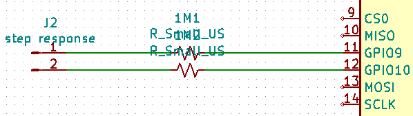
Then I wanted to try some step response sensor with 2 conductors.
I want to try an ESP32, but sadefully there was not any available at FabLab Sorbonne and I could not oreder one quickly. So I select an ESP12F.
CAD - KiCad
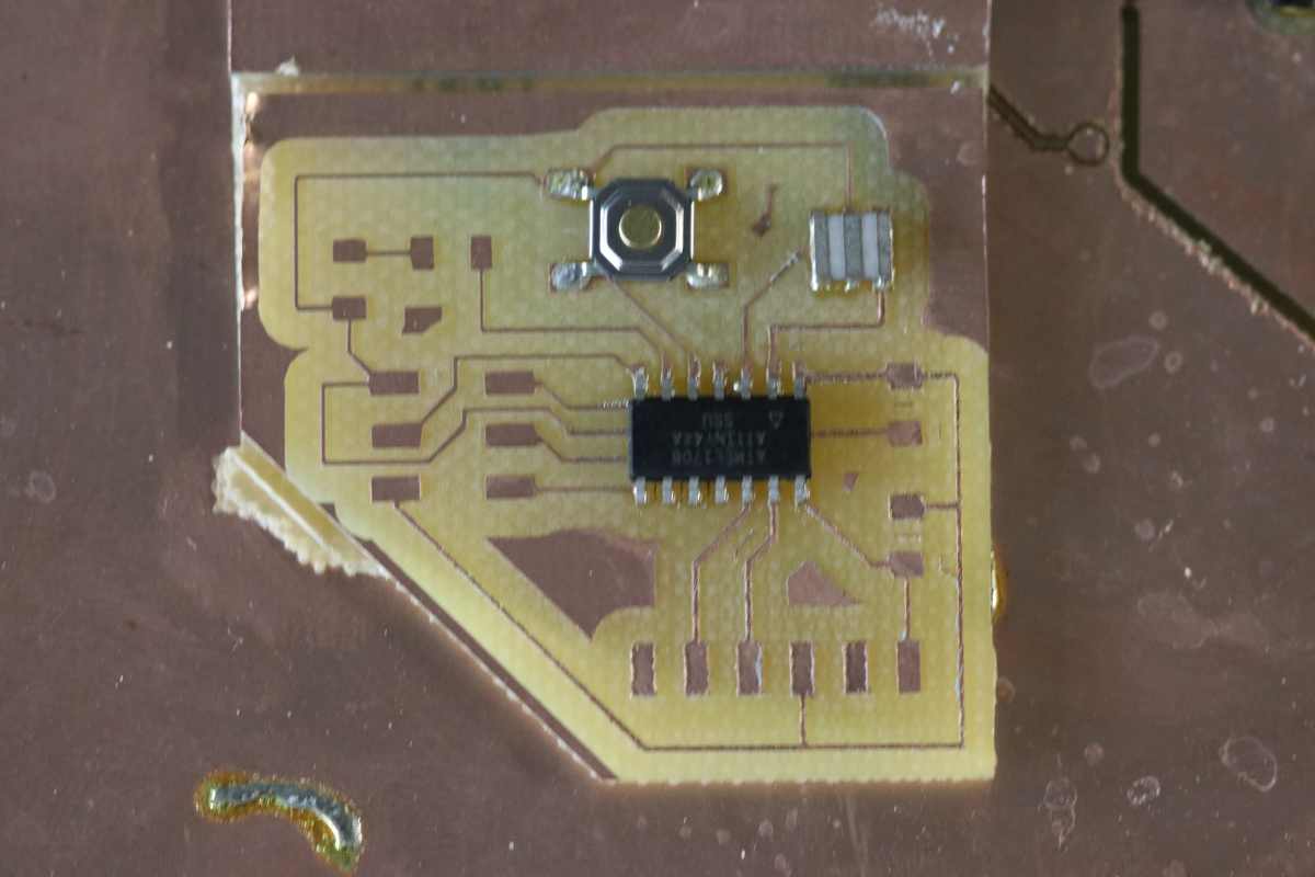
This time I draw the schematic with global label and follow the standard rules of the power in the upper side and ground in the lower side.
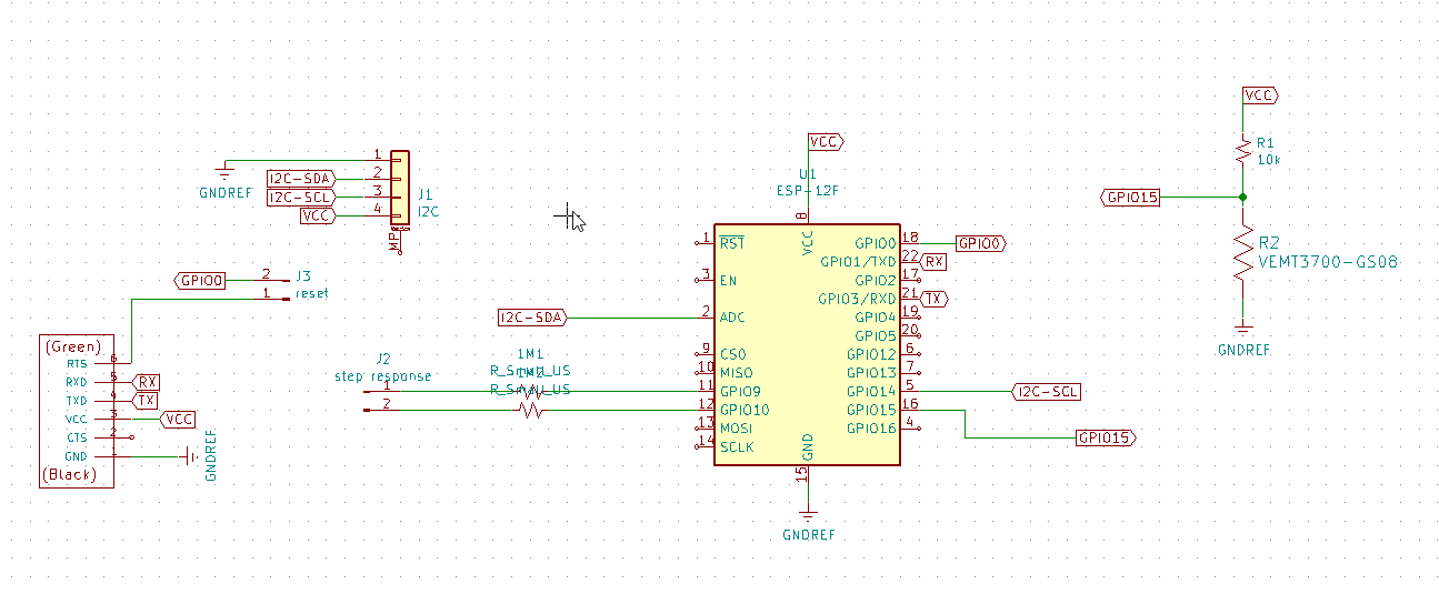
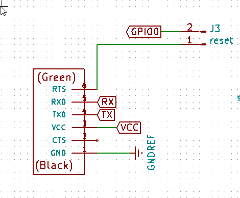
I try to follow other examples for the connection between the FTDI and the ESP8266 to load the program. Things are not clear on the reset pin and th GPIO0, so I put some connector that I can use as jumper. The alimentation of the ESP8266 is 3.3V so my FTDI must be a 3.3V tension, it will also give the power to the board .
I add an I2C connector because the SHT30 that I had is already on a board, and I can’t get the raw component in time.
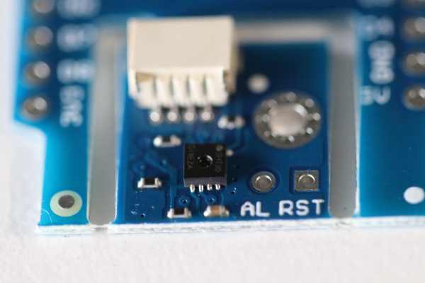
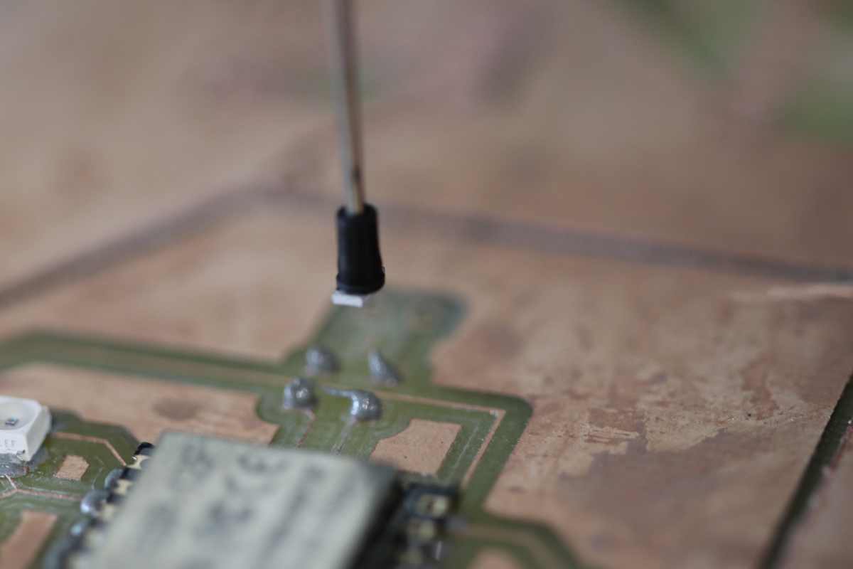
I had to learn how to solder with solder paste. It’s a small component, the connection are extremely small and are partially under the sensor.
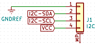
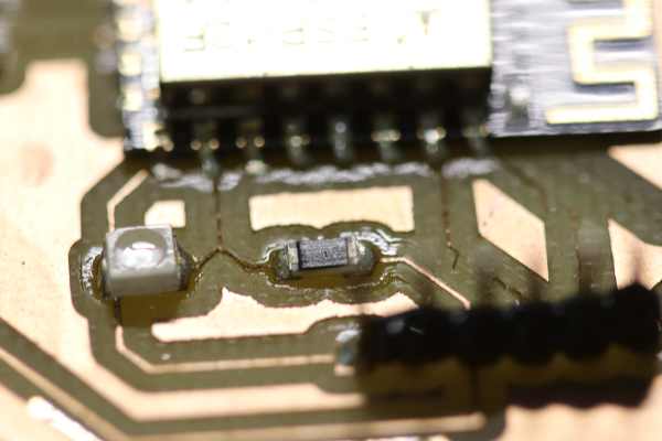
For the phototransistor I had to add a resistor to limit the current.
![]()
For the step reponse, I just put 2 resistor of 1M Ohms and a connector.
Then finding the correct pinout for the ESP-12F. especially for the I2C: GPIO14 is SCL and port2 is SDA according to that documentation : https://www.elecrow.com/download/ESP-12F.pdf .
PCBnew
I switch to Pcbnew to design all the electrical paths.
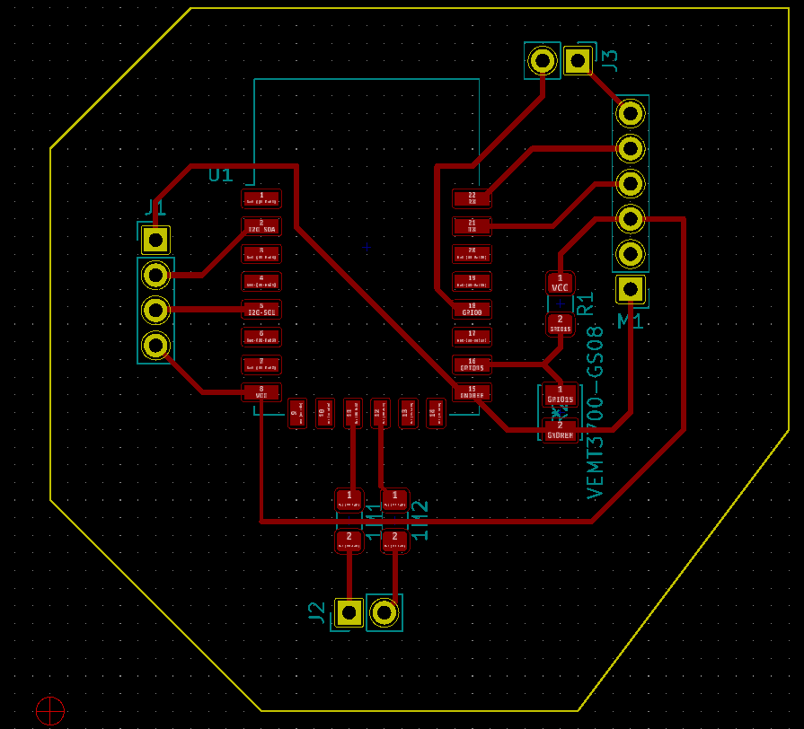
I made the error of making too thin track, I decide to make 0.300 mm, it is bigger than my previous week, but during the milling process some are remove even with 0.300mm . So later I design the track to 0.400mm
To change the track size is a huge amount of work in KiCAD, I did not found a function to select all the track and change the size at once. I have to select them one by one, go in properties and select another size, I try to select several at once, but it failed …
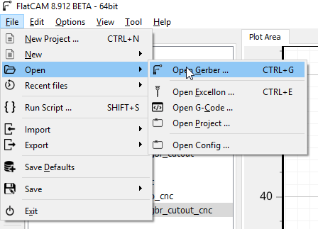
As I have some connectors, I want to drill holes. MODs does not seems to allow those function. For many reasons I want to switch FlatCAM to produce the gcode. I want also to be able to produce gerber files.
I follow a part of this tutorial : https://hobbycnc.com/pc_board_isolation_routing/. But the tutorial part on FlatCAM is too quick, so decide to take the time to understand and explain it in this page.
I need to add a reference point in PCBnew, it’s called axis origin. It will be the origin for the CNC milling.
Then I click on plot .
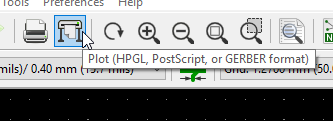
It opens some parameters
To produce gerber files for FlatCAM:
-
I select the 2 layers : F.Cu abd Edge.Cus
-
I check the exclue PCB edge from other lagers
-
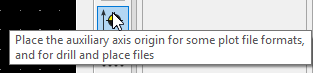
I check use auxilary axis origin”
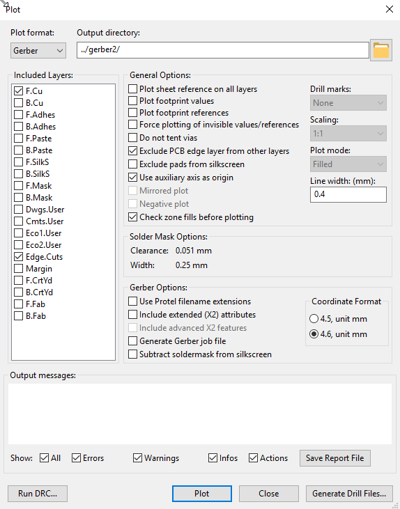
and click on Plot then on Generate Drill Files that opens another pop-up
I select Excellon in the file format and click on Generate Drill File then click on Generate Map File then click on Generate Report File.
So finally I have a bunch of files…
FlatCAM
I open Flatcam , it needs a certain times to acquire the workflow of this software.
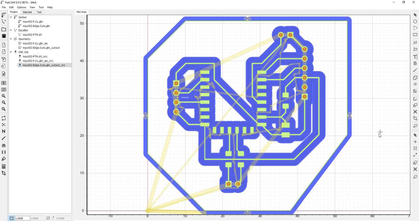
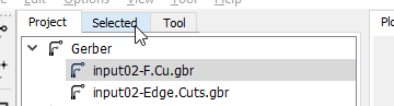
The first thing to do is to open your gerber files created with KiCAD.
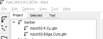
Then they appear in the project under the gerber section.
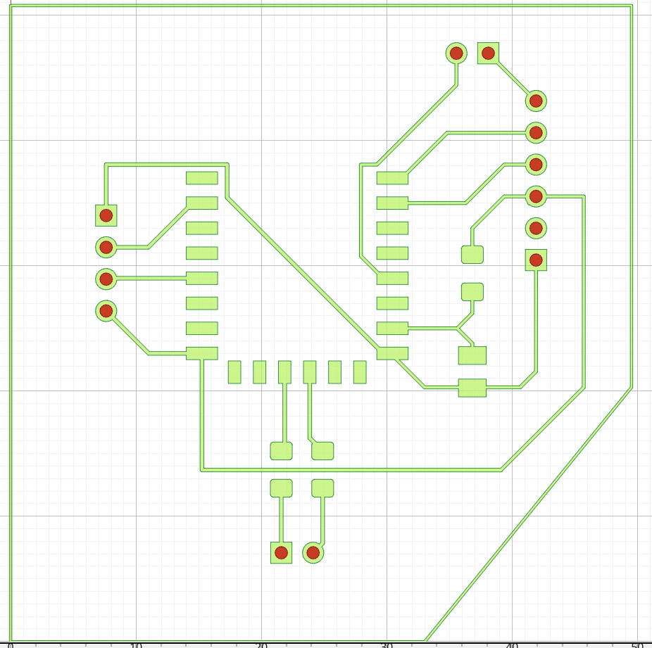
And you visualise what you did on KiCAd.
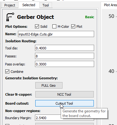
Then you have to select your gerber file and click on selected.
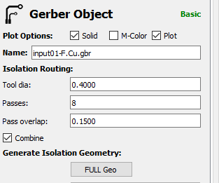
It gives you the parameters .
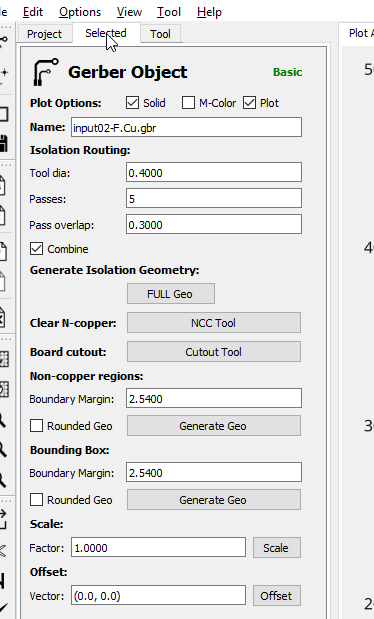
The tool diameter, the passes (the number of tool diameter around your track), the pass overlap, don’t forget to check combine otherwise you’ll get plenty of files…
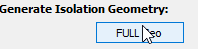
To confirm click on FULL Geo.
It generate the geometry around your tracks.
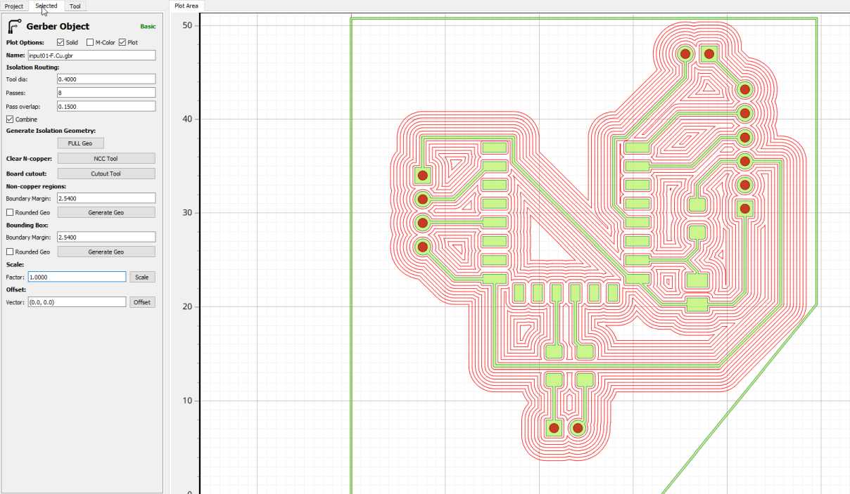
You then have something new in the tab project inside geometry
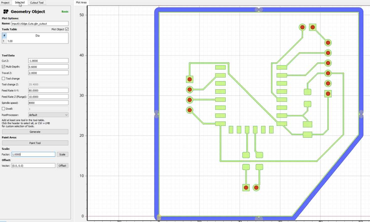
So the logic of the software is to select that new part and click on the tab selected
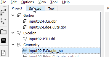
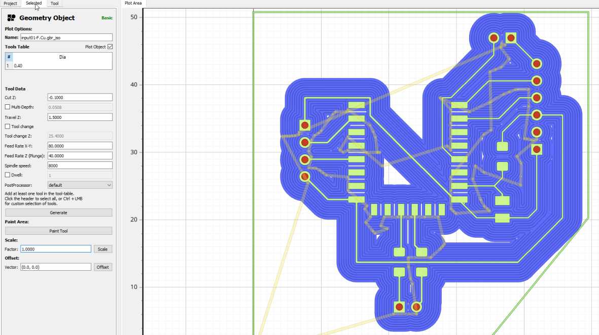
wich gives you access to other parameters.
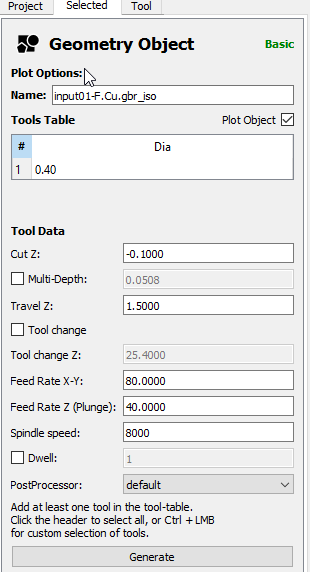
like the tool size : 0.4mm, the depth of the Z cut : -0.1mm. Pay attention the feedrate are in mm/min. The last step is to click on generate.
You then see in blue the tool path.
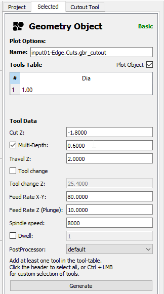
But their is one last step… So again go back to the project slide, select the new file under the CNC Job and click on Selected
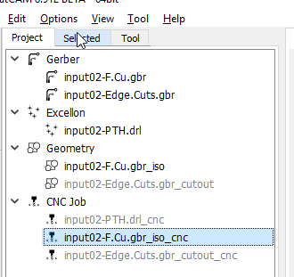
you have access to parameters
click on save CNC Code and you can save the .gcode.
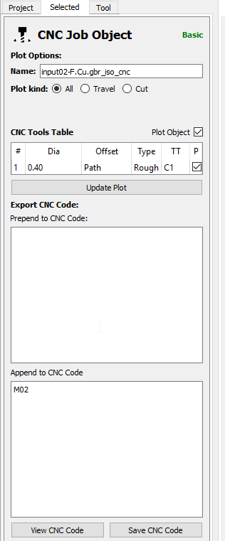
I wont go in details for the rest of the processus, but the logic is the same: you have to click a lot and switch between project and selected .
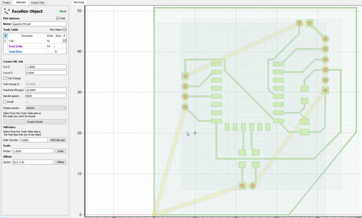
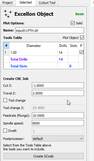
To drill the hole you have to open the Excellon files
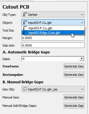
For the cutout you need to select another option and the correct gerber file !
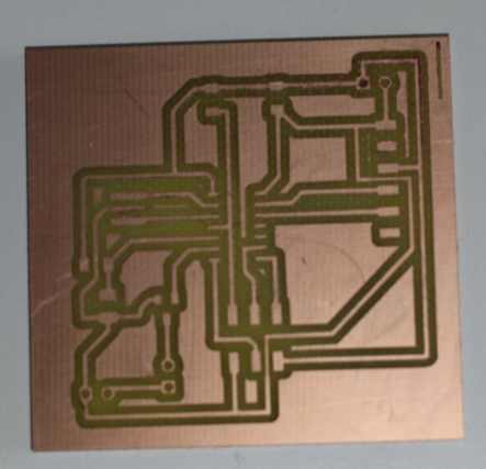
CNC milling
I skip all the explanations , take a look at the previous week. Here the result :
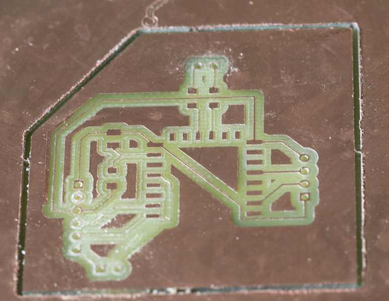
The track are too thin as explained previously but I have a lack of time to produce another one. You can also see the drill for the connectors.
Solderpaste and pick&place
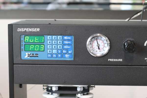
I have a XKAR XMP-300 pick and place with many options. https://www.bomir.com/online/,177,XMP-302D.html
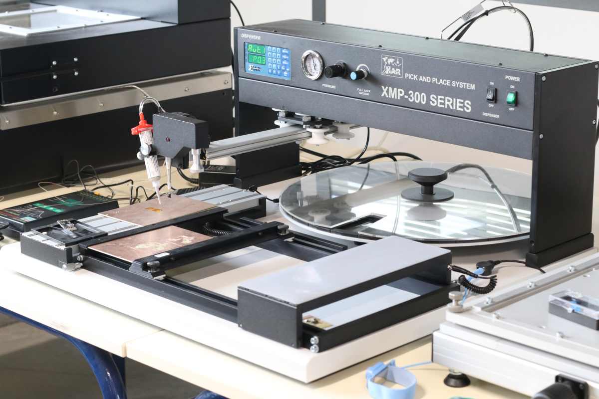
I want to use the manual pick and place and some solder paste. This system is composed of several parts.
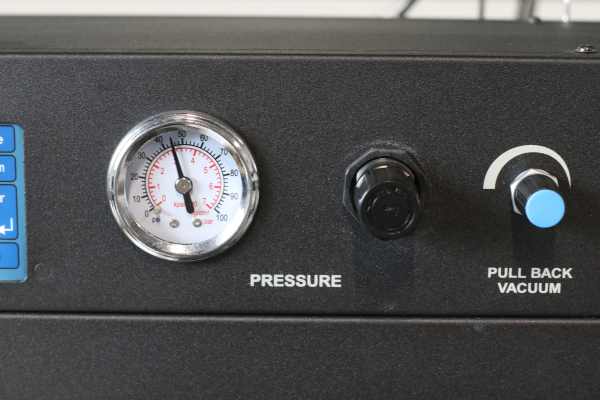
A vacuum system to hold and position the components and a controled syringe that dispense solder paste. You can adjust the vaccum for the pick and the air pressure to push the solder paste out of the syringe.
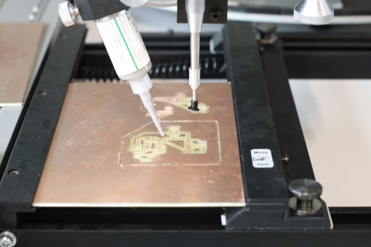
This command allow you to precisely controle the paste dispenser, they are several modes and you can adjust the amount of paste.
With your hands you guide precisely the syringe and with your foot you press a foot remote do dispense the paste, depending on the mode one press will dispense a small drop or as long as you press it will continously dispense the solder paste.
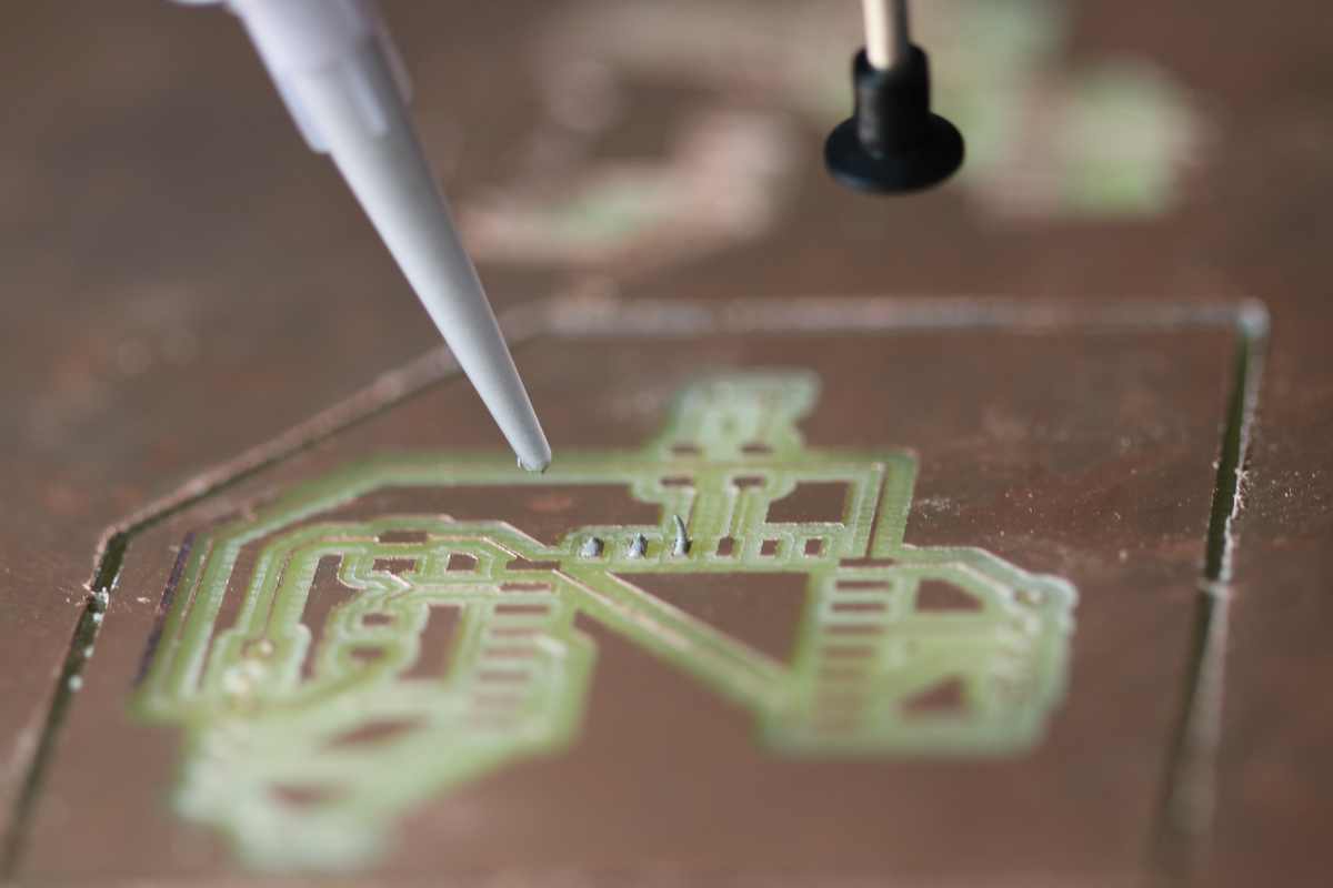
With the pick, I grab the ESP12F. With a knob you can rotate precisely the component and position it just above the place the footprint.
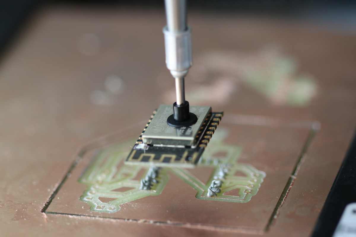
Then you pinch it on the board and it release the vacuum.
They are several size of to grab the components. It’s pretty handy for small components like resistors.
Oven
I use a hight quality oven for soldering, an X-reflow 306 LF with the nitrogen option (not installed, I use pressurise air to cool down) . http://www.bokar.com/x-reflow306lf-ac.html
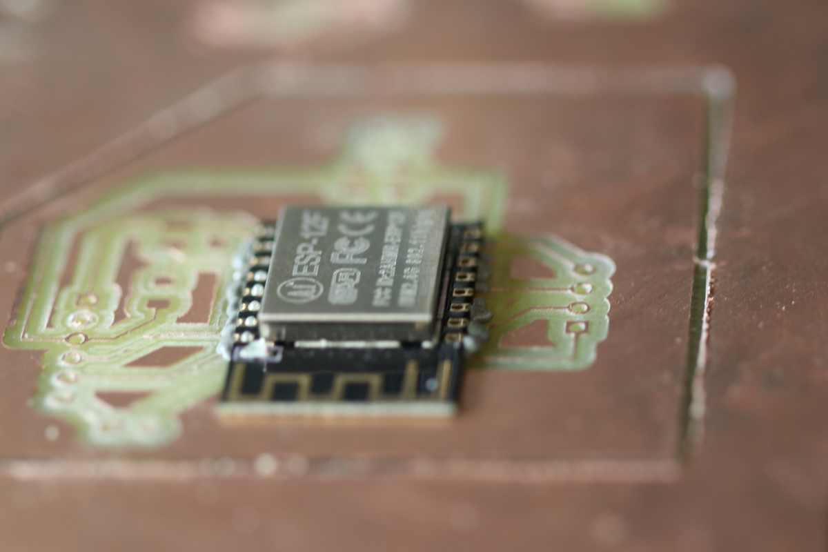
I make a first test on a board that I made on week 7.
Everything went fine. But I tought first that I need to put a small amount of soldering paste, but I should put more.
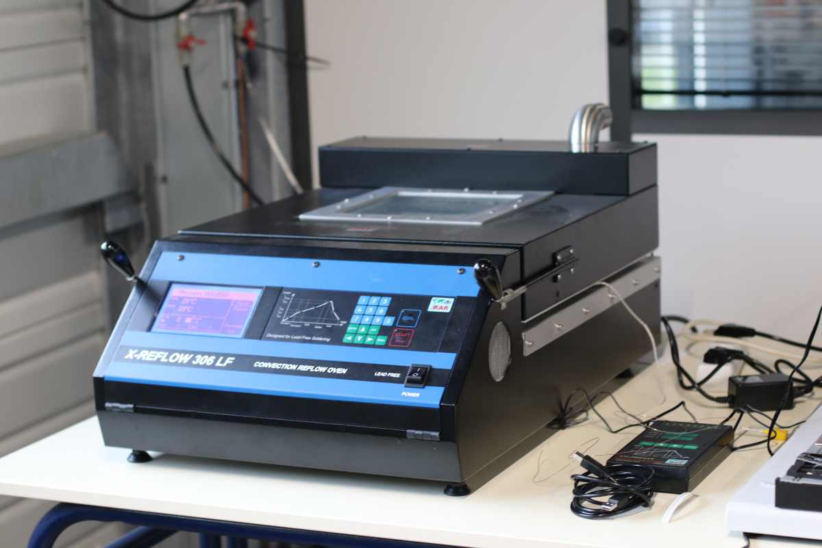
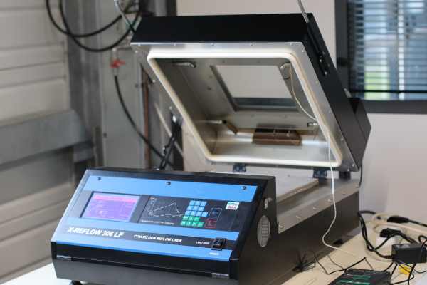
The oven open from the top side .
You can follow a precise curve with differents durations.
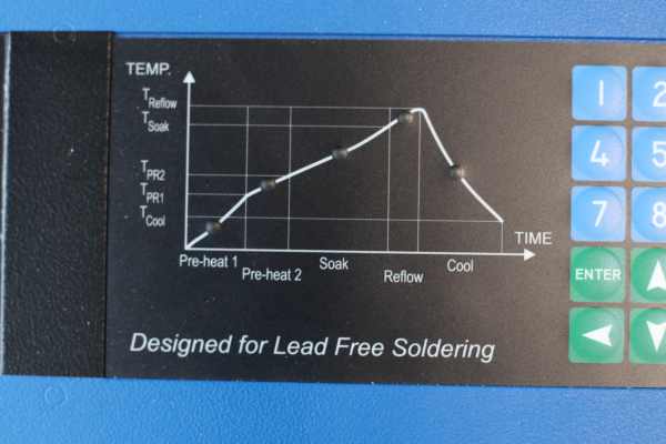
On a screen you can build your baking program, follow every steps and temperature or go to the next step.
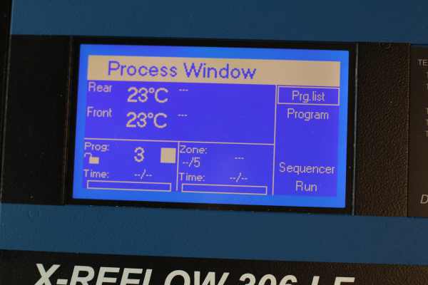
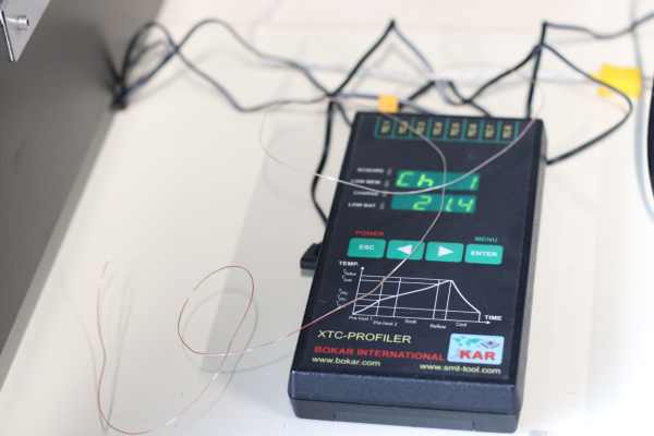
I place some temperature sensors on the board and attach them with Kepton tape. That way you measure the temperature of your board and not only the temperature of the air inside the oven (2 indications : front and rear temperature) .
You can actually see throught the window the paste melting and soldering.
I saw that not everything melt and solder at the same time. Some part take a longer time.
I made the mistake to put the connector in the oven. The plastic at the bottom of the connector partially melt. But the rest seems fine.
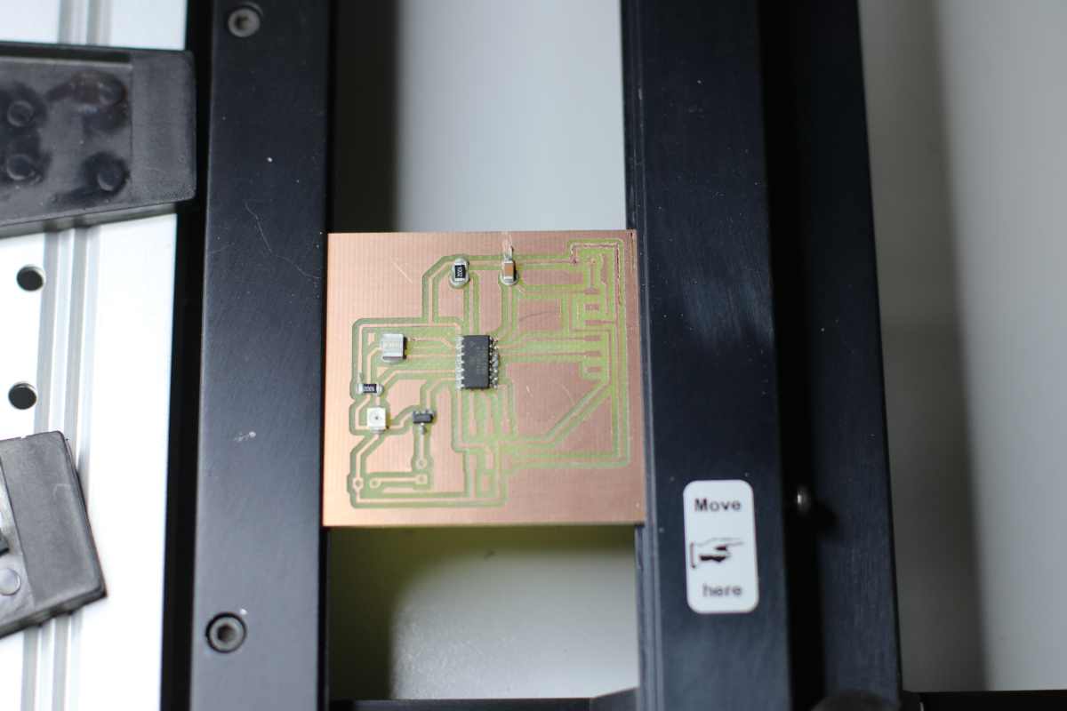
As you can see on the pictures the components are corretly soldered. But some tracks were too thin and some have disappeared as described above.
PCB result
With probes, I check the connectivity of the components to the footprints and to the end of the tracks, the soldering seems fine. But some tracks are missing from the milling process .
Not finished
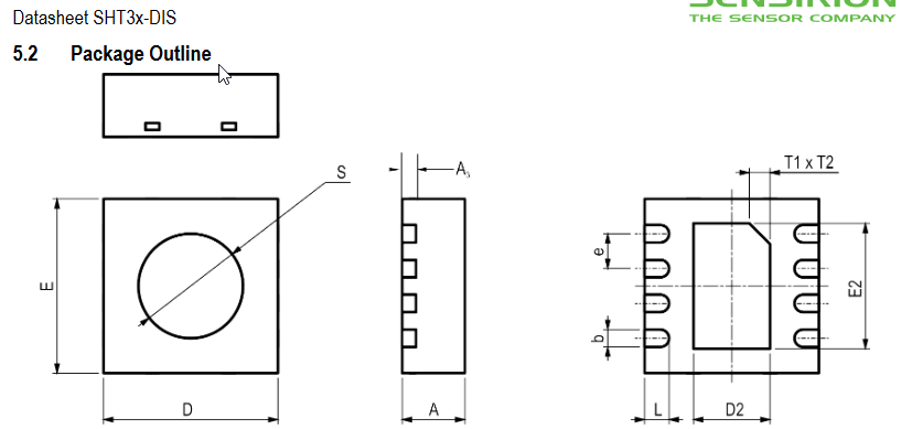
But times was leaking and I did not finish this board. I lost a lot of times finding the footprints : - in KiCAD, I did not find the VEMT3700. I look a lot on the merchant MOUSER, then with SnapEDA - I switch then on Eagle, but lost a lot of time trying to find ESP12F…
Finally I get back to KiCad and found the VEMT3700 footprint on another merchant page …
I have not finished the board but I learned a lot of things :
-
I try FlatCam to produce the gcode
-
I read on the esp8266 , and the several sensors
-
I solder, with solder paste and an oven
I finish the assignement with another board based on a AtTiny and describe it below .
Group assignement
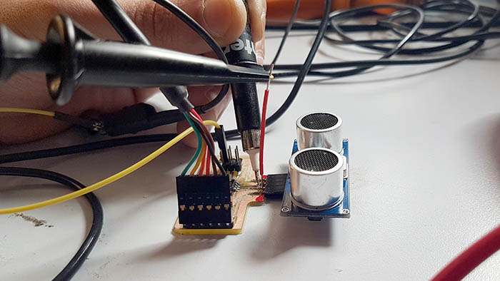
For this week, we decide to test the ultrasonic sensor HC-SR04.

Characteristics
Measuring range : 2 cm to 400 cm
Measure resolution : 0.3 cm
Effective measurement angle : 15 °
Trigger Input Pulse width : 10 µs
How to use it ?
To trigger a measurement, a “high” pulse (5 V) of at least 10 μs must be presented on the “Trig” input.
The sensor then emits a series of 8 ultrasonic pulses at 40 kHz and then waits for the reflected signal.
When this is detected, it sends a signal “high” on the output “Echo”, whose duration is proportional to the measured distance.
Measurements
We connected Julie’s board to the FTDI to power our sensor and then we started measuring with the oscilloscope what was going on.
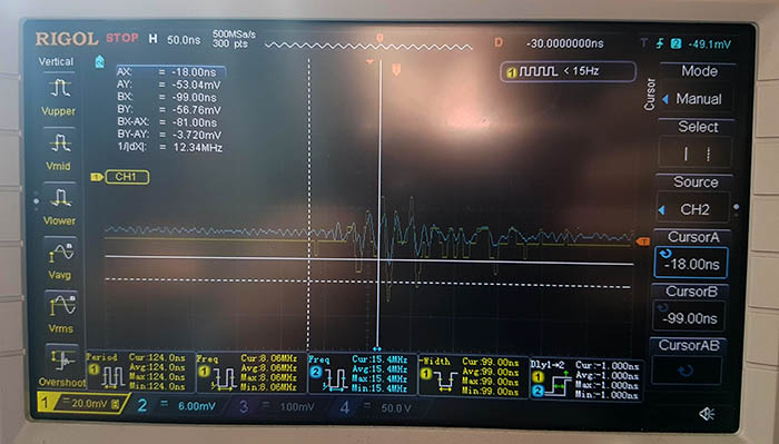
This is what we observed on the oscilloscope. We can clearly see a little delay between the 2 signals. It’s the time the signal takes to come back to the sensor.
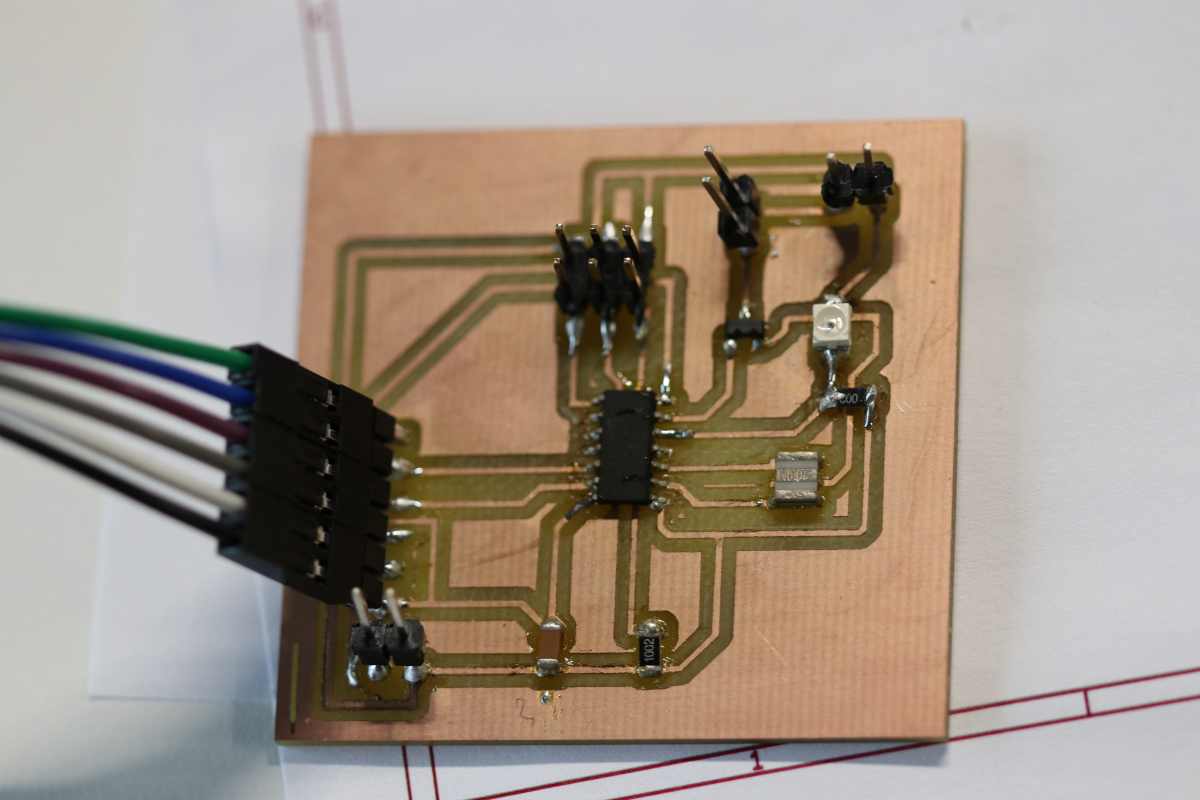
Finished
I finish this assignment on Week 12 . I put below the result.
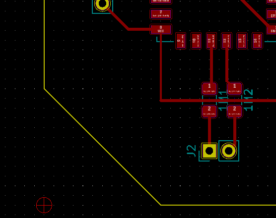
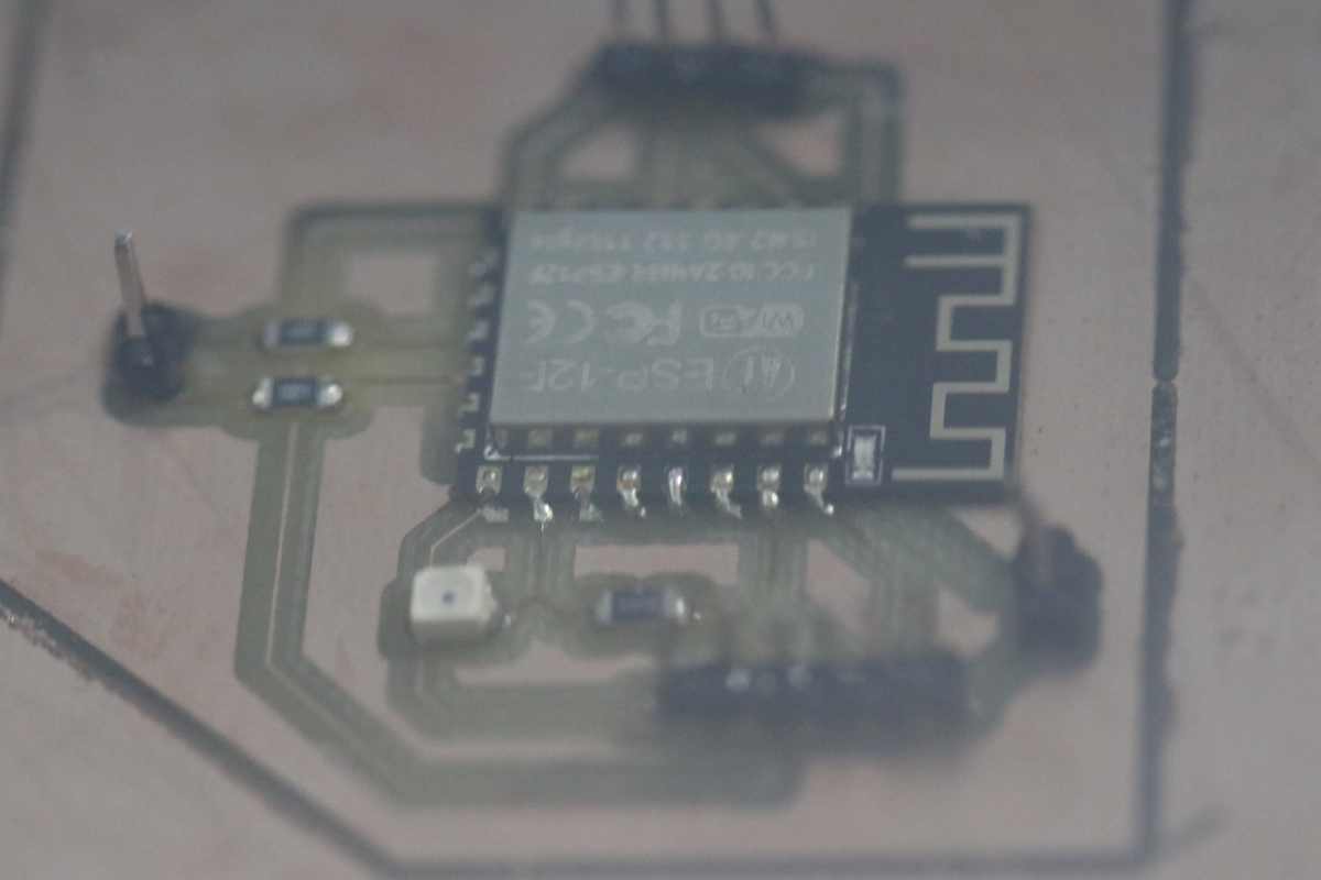
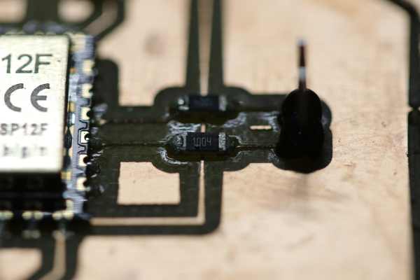
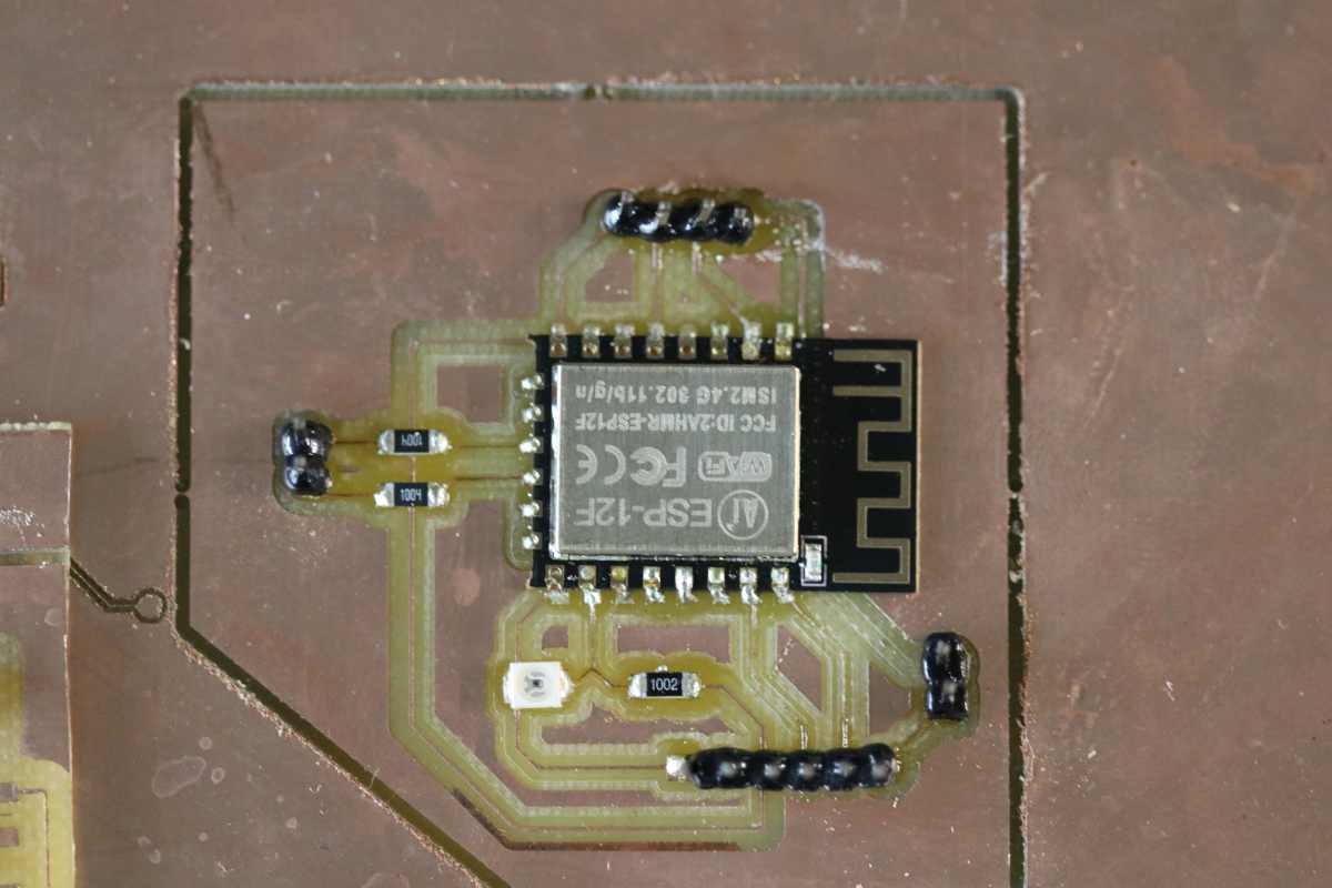
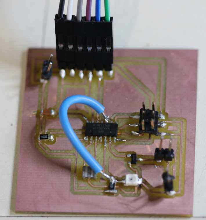
For the Phototransistor, I have a VEMT3700. I had many problem with the footprint and kicad. I had to select another component to have the correct footprint ! So it looks like a resistor but I will place the phototransistor in the correct orientation.
![]()
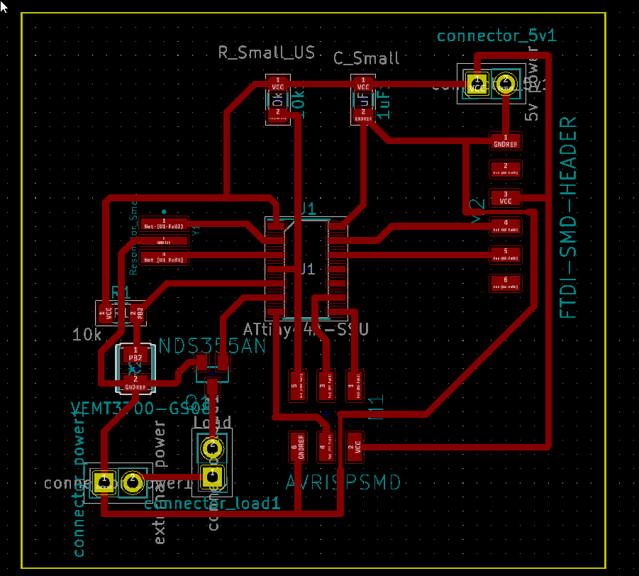
Trace
My trace.
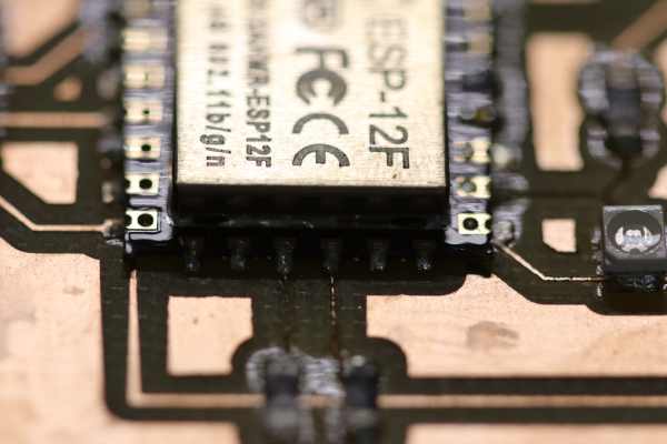
PCB Board
I do not detail the whole process for the milling of the board. Take a look at the previous weeks.
I use solder paste, pick and place and oven .
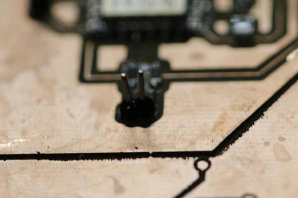
This time I have not made the mistake of putting the connector with plastic part. I know it will melt in the oven …
Then I solder the connectors and check all the connections.
I made the mistake of connecting the phototransistor on PB2. This pin does not have an ADC.
I solder a wire connection to PA 3 and it works now , I can read the value.
Code
The following gives changing values : read-photo.ino
#include <SoftwareSerial.h>

//TX , PA0 , could be A0, 0 , 10
//RX , PA1 , could be A1 , 1 , 9

const int mosfet = 7; // connected to PA7 or 7 in arduino
const int phototransistor = A3 ; // connected to PA3 , A3 in arduino

int photovalue = 0;
int timing = 50;

SoftwareSerial mySerial(0, A1); // RX, TX

void setup() {
  mySerial.begin(9600);
  pinMode(mosfet, OUTPUT);
  pinMode(phototransistor, INPUT);
}

void loop() {
    photovalue = analogRead(phototransistor);
    mySerial.println(photovalue);
    delay(timing);
}
When I put some bright light on the phototransistor , the value move from 1010 to 20.
The video of the board working
That day, the sky was cloudy the average value was around 920.
When I put some bright light, the value goes to 20.
When I cloak the phototransistor with my finger, the value goes to 1000.
Then I approach slowly the light to the phototransistor to see the slow shifting in values.
Conclusion
After milling some boards, I’m sure that my workflow is better. But I still had many fails.
I’m now in great doubt of the quality of the FR4 copper plate. I think the thickness of copper foil is not equal. I greatly doubt of the specification of 35 umeter.
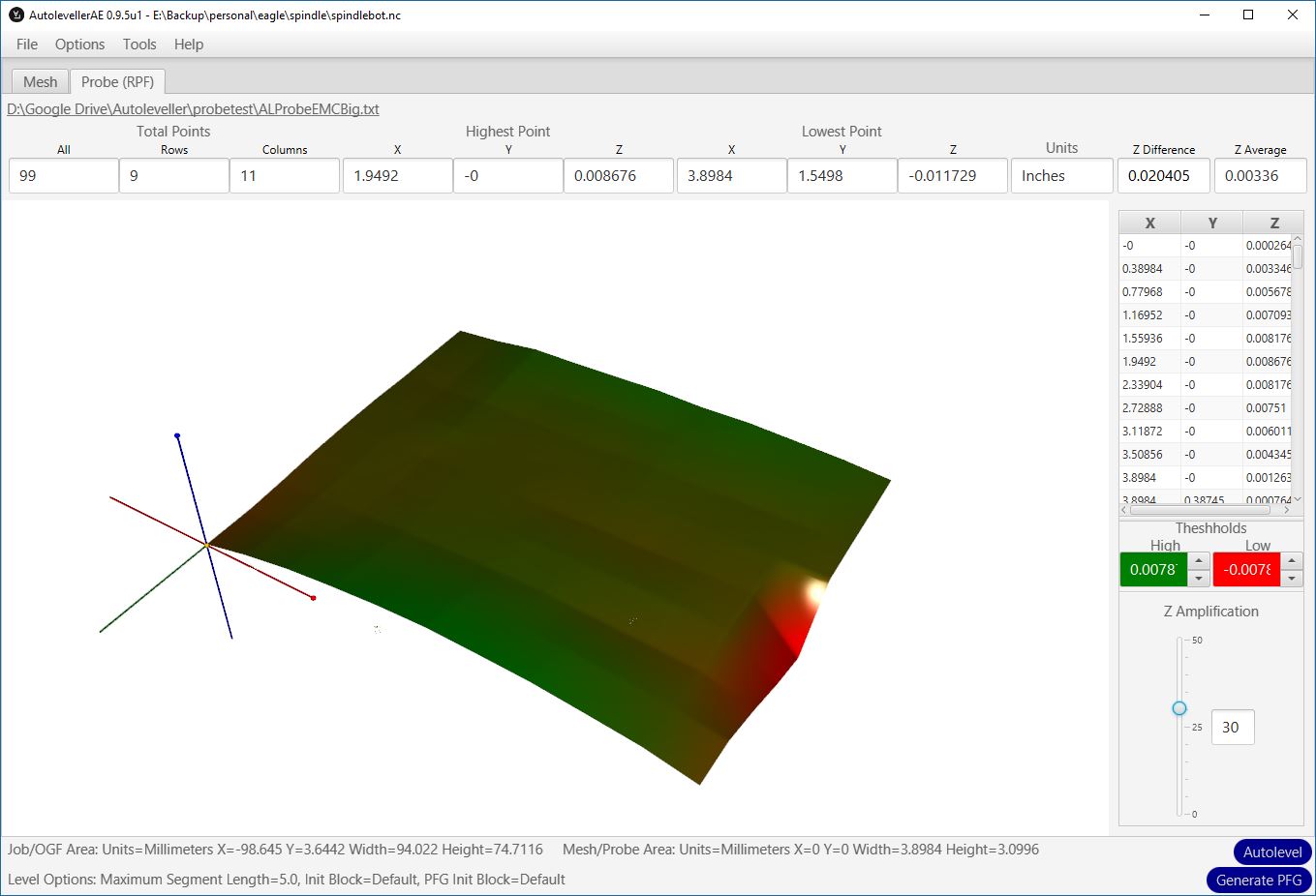
I want to try Autoleveller , https://www.autoleveller.co.uk/, it should save me a lot of work. But the Roland SRM 20 does not seems to have an input for the probe …
I’m wondering if it’s possible to build another controller just to measure the Z variation with a probe by sending directly gcode to the Roland SRM 20. That could build a deviation map of the Z that could be use with Autoleveller to produce a corrected gcode like in this following picture (from the Autoleveller website )
Files
Kicad files : input-kicad.rar or input-kicad.zip
Gerber files : gerber.rar or gerber.zip
FlatCAM file : input004_flatcam.rar or input004_flatcam.zip
Reading of the input of a photo-transistor : read-photo.ino