7. Electronics design
This week I have to design an electronic board with an atTiny44 , a resonator of 20 Mhz some condensator and resistor, a LED and a button, a ISP connector and a FTDI connector. Produce the board by milling, solder all the components, check them. Test and learn several electronics tools : multimeter, oscilloscope. And finally test a small hello program.
Board design
I install Kicad and add the fabacademy libraries of components.

KiCad is a toolset of several software that are connected to each other. You have to first design the schematic on Eeschema , select the right components. Then you design the layout on Pcbnew. And finally you export in svg to be able to mill the board.
I started with Eeschema .

With read netlist

I place all the components and connect them. You will see later, that I made some error in those schematic.
Then I created a netlist. It’s a file containing all the connections. It tells wich component is connected to another one.
Then I switch to the Pcbnew software. I import the netlist and click. It place all the component and connection in a compact way.

I place the components to be able to read them .

Then I optimise the position and rotations of each of them to simplify the pathway.

Then I route manually all the connections.
I find my first error. I didn’t connect correctly the reset pin on Eeschema . So I go back and modify the schematic.

I go back to Pcbnew and use the update from schematic function. Hopefully it works and I don’t have to redo all the work.

Then I have my first version.

I use the design rules control to be sure I did not miss a connection.

I desing the edge of the board with the polygon tool on the edge layer.

I was curious with the 3D visualisation tool. It clearly did not show all the components. I think I have not all the 3D files.

I’ve done that work in several small amount of times, I was busy during some international Agriculture event. And that’s not a good idea. After a good night of sleep, I check again the design.
I print on paper the layout to check it. Clearly the resonator was not the good model in the library. The resonator was not by default in the libraries. I have to find it in other libraries and install them…

I find also that I missed to add a resistor with the LED .

I have to update everything in Pcbnew , replace and reroute some components.


Finally I export in SVG format .

Board gcode
I use mods to prepare the gcode. I open the svg in an another software to look at the file.

Then in mods I select the right program to process svg with the milling machine.

I had to invert the black and white.

Specify the origin and speed .

Specify the right diameter tool .

And add a save file module .

Then I produce a gcode.
And have done another one for the cutout of the border with a different tool diameter.
Errors
I made several errors. First I didn’t find visually the error with a gcode path. It didn’t cut correctly a path, 2 paths were merge.

The path on kicad are too close. So the rules for the path distance are not correctly set.

I check with a multimeter and find some short circuit …

I delete the path and make a new one with more space between the path.

Then I made an error with the cutout. I had to use a 3.0mm drill for the cutout and it destroy some path. So I design a cutout farer of the paths.


Design Rules Editor
I take extra times to try to undertand the Design Rules Editor , the default values do not work for the machining with a 0.4mm bit .

A clearance of 0.2 mm can not work. I modify it to 0.4 mm
Here is the differences :
![]()
The red arrow show some problems, the path are too close to some pads.
![]()
With the new design rules editor I modify a lot the path of the track to avoid all the problems. I also modify the grid size for the path.

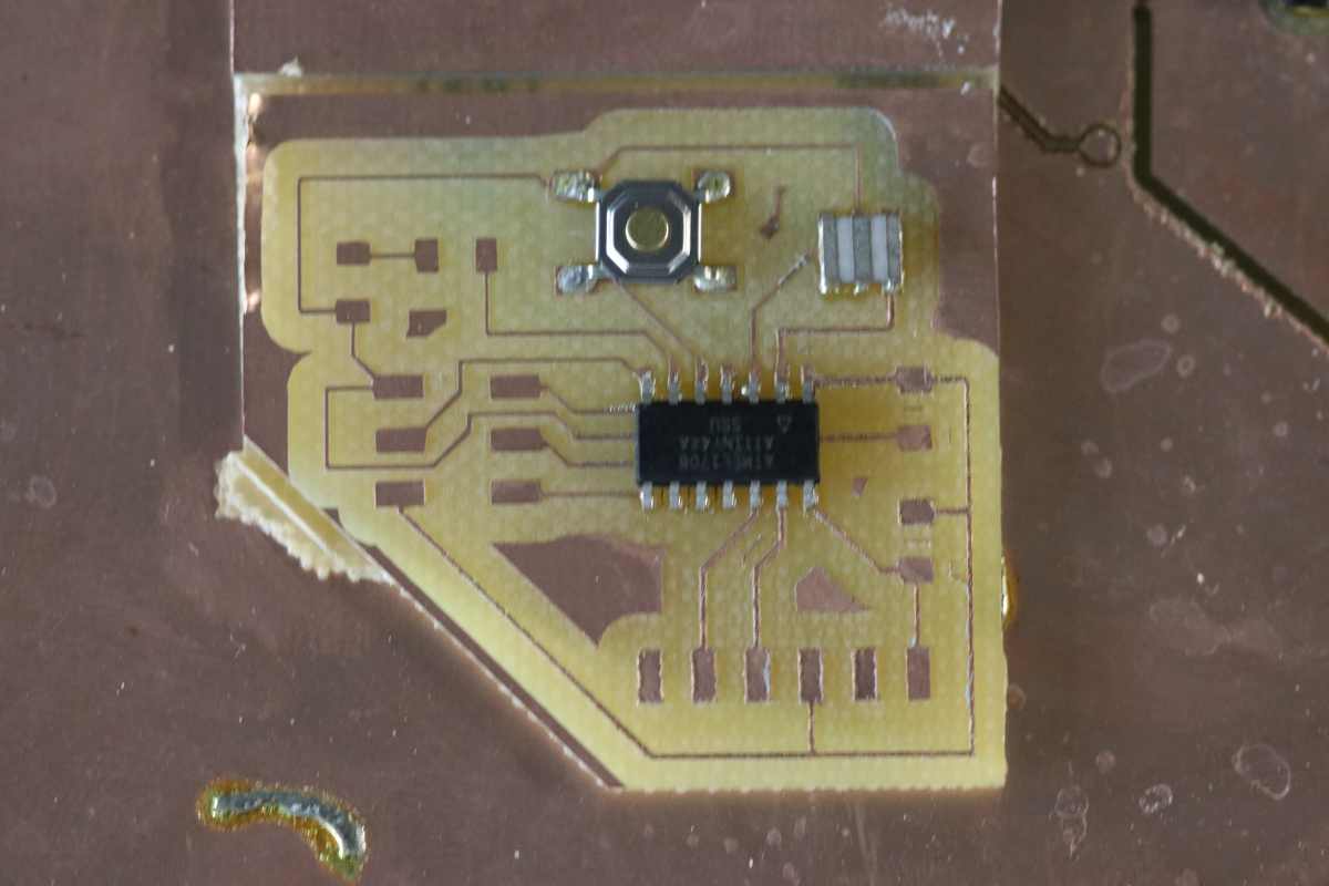
Board
Finally I produce a Board.

Some tracks are too thin. But I no other choice, time is missing …
I solder the components and add 2 flywires to fix some tracks that were too thin and has disapeared.
On week 09, I described how to program the Board.
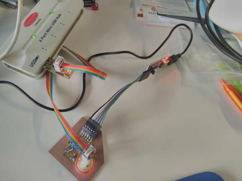
On week 11 , I used another copy of this board to try the solder paste, pick and place and oven.
Remarks on KiCad
KiCad is growing in a great tool. It is open source. They are many usefull tutorial and you can build simple pcb, and go really further without any limitation and build complicated multilayer PCB. Opposed to this you have Eagle, a big renowned software. Autodesk own now Eagle. You have access for free to a limited version of Eagle : 2 schematic sheets, 2 signal layers, and an 80cm2 board area. For more you have to pay.
KiCad has really evolved especially since version 5. I am using verions 5.0.2 so the following comment will be outdated soon :
ERC in KiCad
ERC is a tool that should prevent electrical mistakes like shortcut or missiong to connect the ground or the power. But at this stage it is really messy and find problem where they are none …

Just click on run . You have then a list of delcared problems.

In the background arrows point the potential problems. If you double click on elements in the list, it show you a close up of the schematic part.
Just to illustrate that this tool is not yet ready, I select one “error” , I connect a ground to a ground . Their is no error.

Then other potential errors …

Here also thei is no error.
Till this tool evolve, you should consider to check Electric Rules by your own …
Conclusion
Don’t try to do to thin traces. I will make the mistakes again on the following weeks …
Files
The last version of my kicad files : simpletiny44.rar size 23ko , and a zip compression simpletiny44.zip size 24ko