Week 7 - Electronics Design - Part 3 - Milling and Soldering
Redraw the Echo hello-world Board
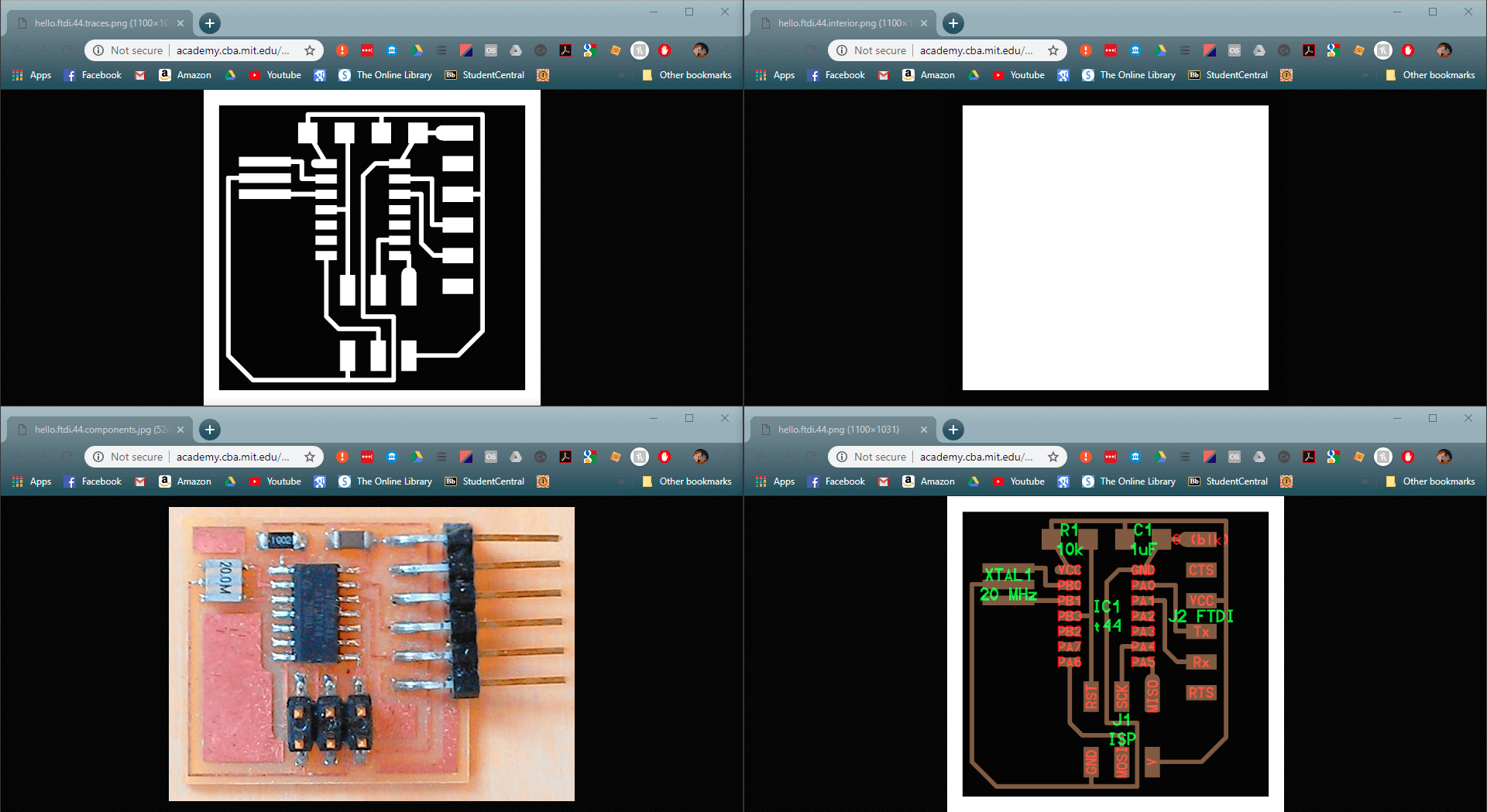
These are the example files for the board, it is required to add at least an LED and a button.
Milling
I have come into the lab to do a second round of millong on the MDX-50, I prepared the .rml files the other night so all that should be required is to set up the machine and get cutting.
I ran into many errors and setbacks during the manufacturing of the board process, the frustration I felt from not being able to create the board let alone get to programming.
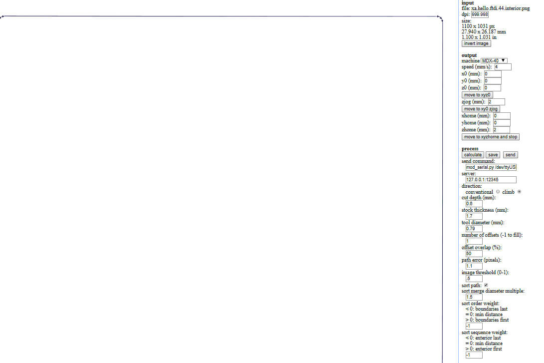
Initially I had setbacks with fabmodules and dpi settings resulting in very wrong size outputs on the .rml files.
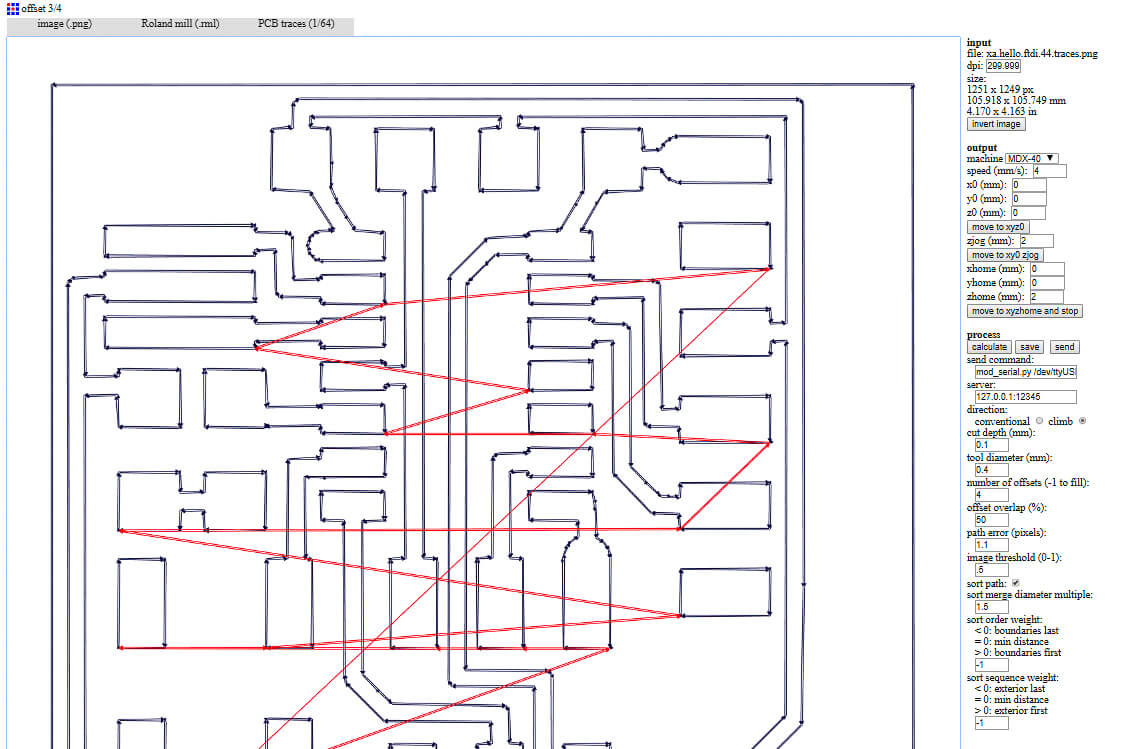
notice the size and dpi settings in the top right.
I didn't
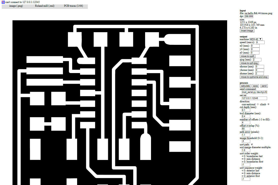
the right angled line displayed here.
Conversely I had the opposite error with the outline for the 'fixed' size board.
this led to the destruction of external traces during the milling process.
Not only were these size errors time setbacks. When I had a board in my hand ready to attach parts, and botch a solution to the missing traces.
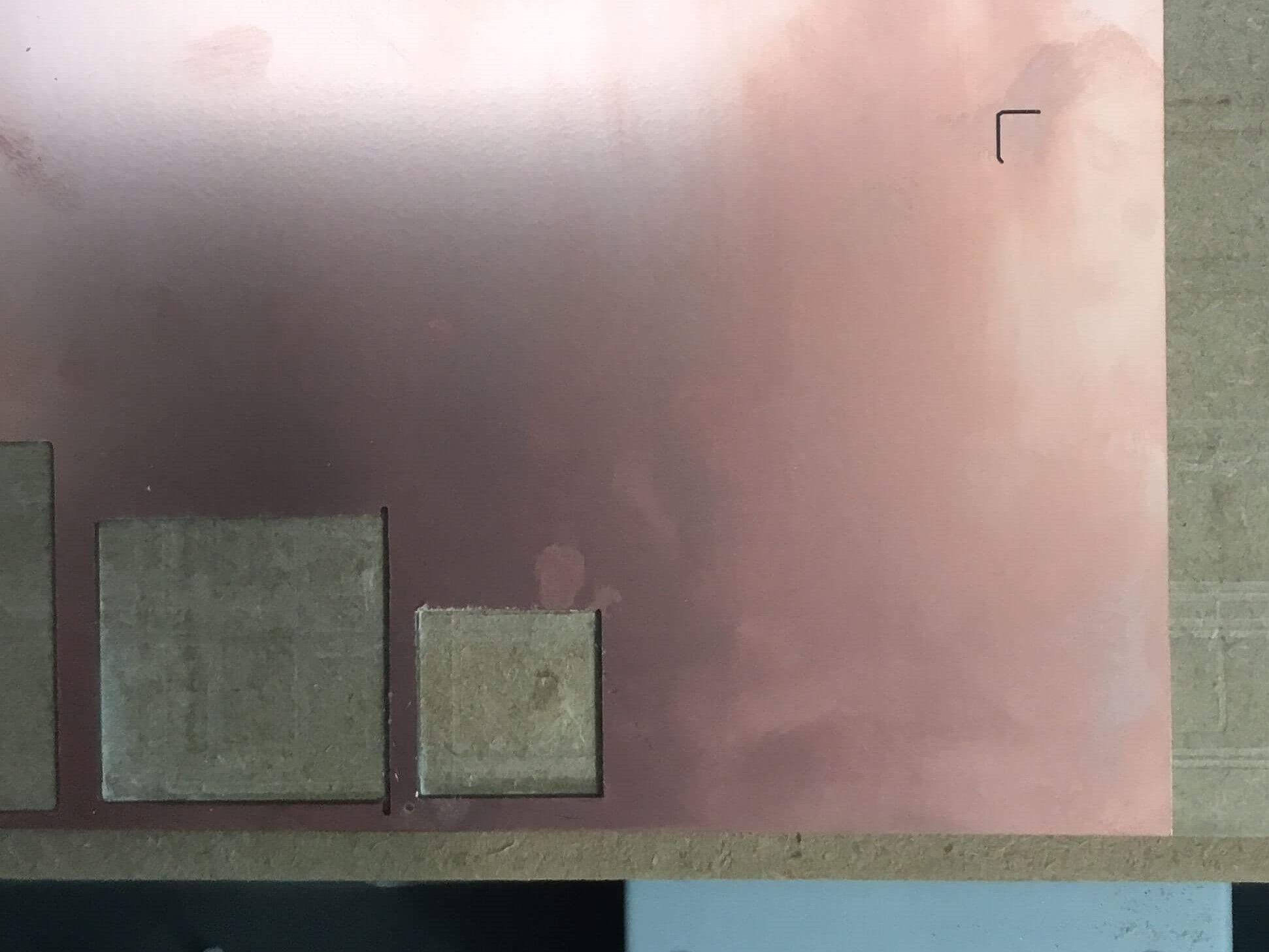
The scale must've been wrong somewhere along my process through illustrator using the example files as sample's to create more circuit.
The pads are the wrong scale, it isn't much but due to the size of the components this has created a major issue and requires a complete redesign.
I am going to do this in Eagle following a tutorial to better understand the schematic and board relationships within the program.
So I made a mistake on the outlining of my board. It isn't required to have a white border on the trace file, as that just creates more work for the tool creating what the outline cutter is for.
I reopened the original illustrator file, deleted the white border box, re-exported the asset making sure to export at a resolution of 1000dpi to import into fabmodules for rml creation.
This time I had some success milling the board, but it started doing what looked like the end (it wasn't), or an error (nor that), so I cancelled the end of the cut and removed the part.
Only to see that it had in fact not finished milling.
I checked the machine code output by fabmodules to realise it was milling a border or the traces layer (which is what I cancelled in the middle of - missing the milling of the rest of the board)
So I fixed that and set the board to cut again. This time with success (very almost).
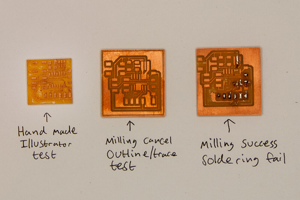
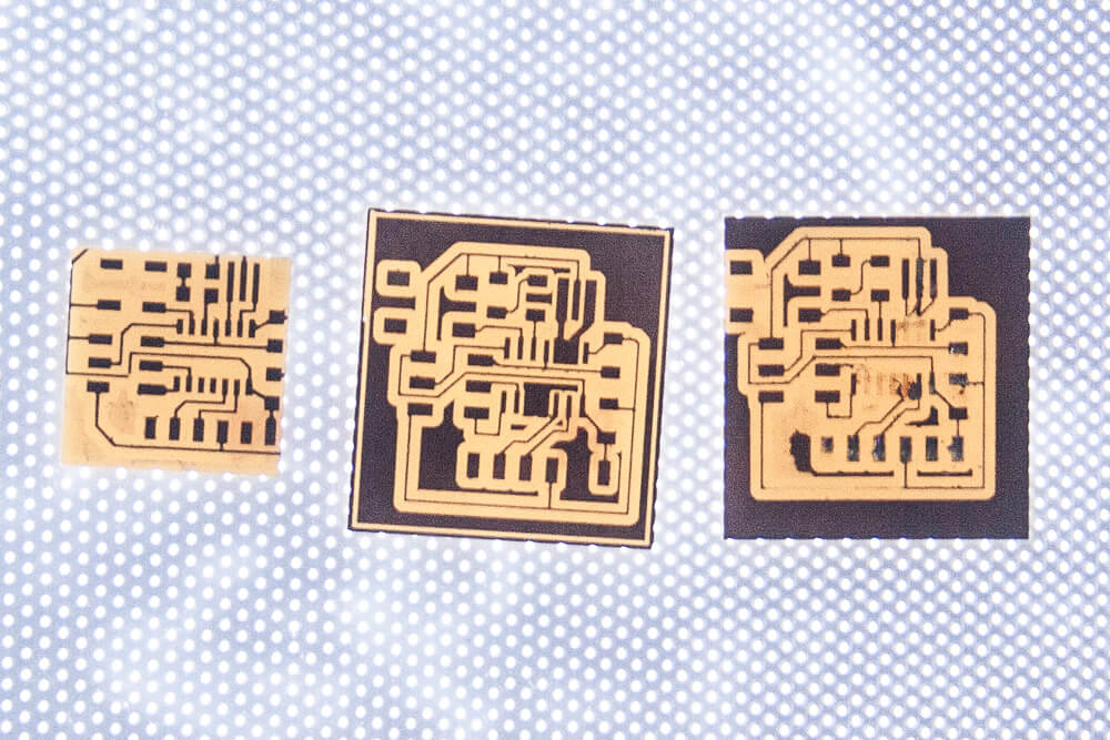
I photographed my boards on a lightbox to show the traces as well as possible. On the far left is my first board (failed from outline)
The board in the middle is the one I cancelled mid cut so has incomplete traces and pads.
The board on the right is the one that got the closest; I think this failed due to the traces being too thin; or possibly due to the soldering iron I have at home not having a proper temperature regulator so it just burned the pads off the board.
So it was time to head back to the milling machine - I widened the traces slightly in file (Illustrator stroke width).
I also edited the offsets setting in fabmodules - this should lead to the tool cutting fewer paths around the traces leading to there being more copper left over; I just reduced the offsets from the default four to three.
So the editing to the offset setting did do something, the traces didn't just immediately disintegrate under a sanding block, although I was still losing the VCC trace on the boards side.
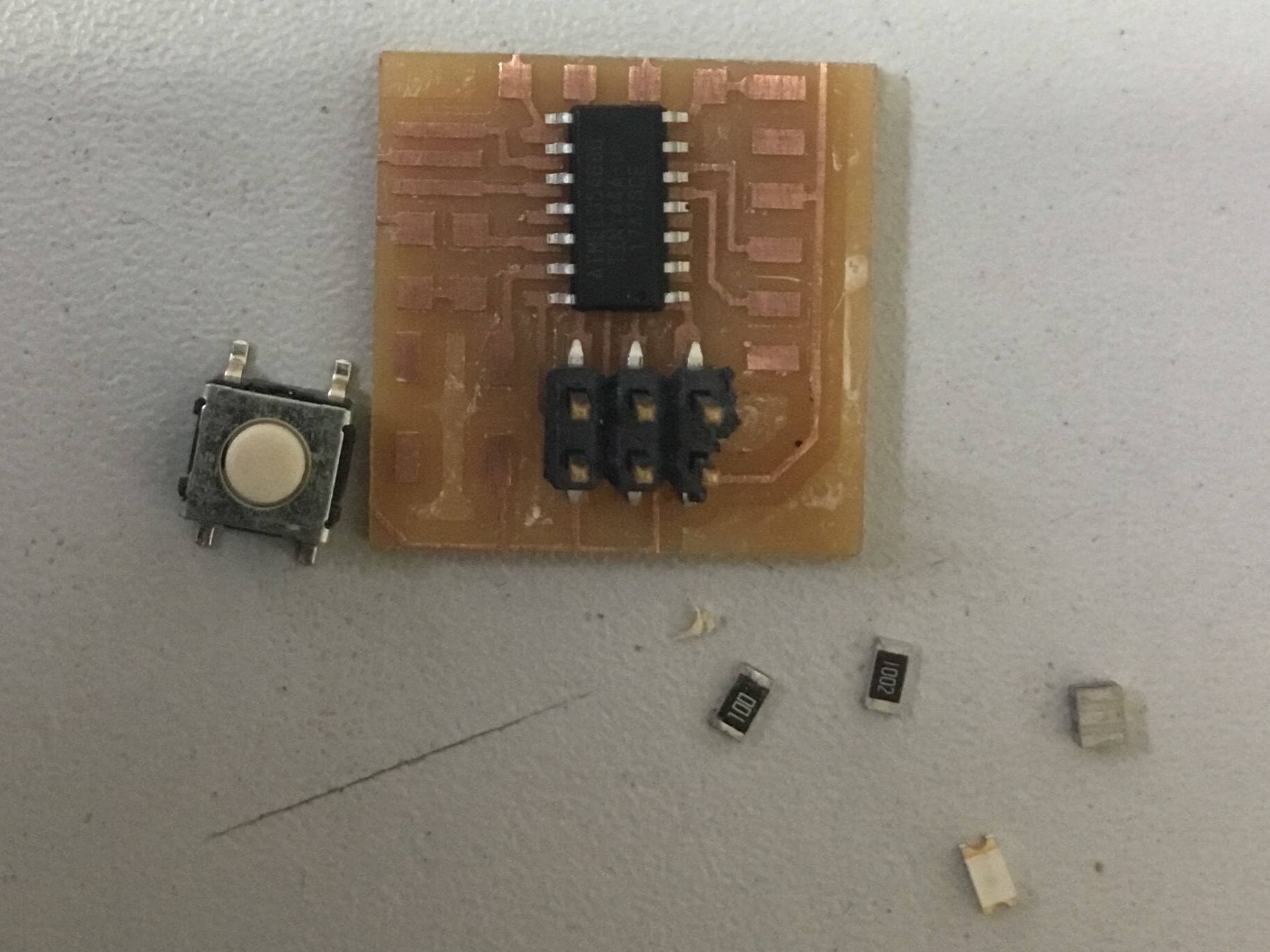
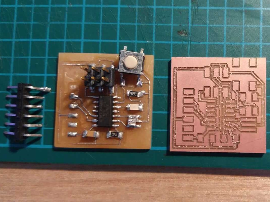
I decided to use the board anyway to practice my soldering as I had had problems destroying pads with the soldering iron with my previous attempt.
This went fairly well, but I still need a better method and more space to solder on - it could also benefit the process to scratch the copper surface to allow the solder better grip.
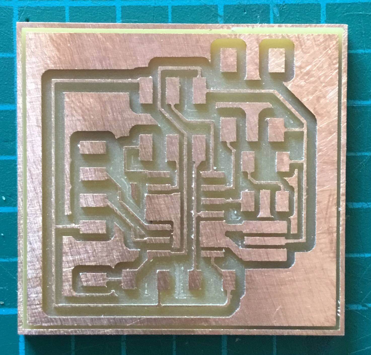
The board on the right is the most recent milling attempt - this has an offset setting of 1 instead of 3/4 as was used in the past. This will require significantly more board cleanup with the removal of excess space, and the sanding of burring along the traces.

Here is a side by side progression from left to right of my board creation process (This is taking a lot longer than I was expecting, which is rather frustrating).
So I now have what should theoretically be a functioning board.
All I need to do is get to programming.
This might end up being split into multiple documents now.
Windows and Windows Problems
In summary Windows sorta sucks
there are problems with driver signature permissions in Window 10 which makes it (at least appear to me) impossible to get the arduino IDE to be able to see the board through the programmer.
Linux and more Board Design issues
So I switched to my little linux laptop at the lab to continue my programming adventures.
This time I followed Michaels website as a tutorial through creating the programs and files needed to do the programming.
This process was a welcome break to the frustration I was feeling at windows. However after testing a program in the terminal, I turned to copying the blinking program Michael had made, only to find out that I had my button and LED on different port sides of the chip, and that I did not know enough yet to work out how to solve that problem.
I felt at this point it would be easier to return to the software, and design another board which had both the button and the LED on one of the port sides of the chip, namely PortA. This required a switching of the LED connection from PB2 to PA3 with the button staying on PA7.