TASK TO DO:
- Make an in-circuit programmer by milling the PCB.
- Characterize the specifications of your PCB production process.
- I made FABISP board and programmed it.
Group assignment:
WHAT I HAVE DONE:
In this assignment we are going to make programmer board which is going to program other board.
Here all started with Electronics which is almost unknown and new for me.
What is PCB? -
A printed circuit board, or PCB, is a non-conductive material with conductive lines printed or etched. Electronic components are mounted on the board and the traces connect the components together to form a working circuit or assembly.
There are various materials available for PCB printing. We are using FR1 in vigyan ashram which mills nicely and the endmill lasts longer.
FABISP -
Neil introduced 4-5 types programmer to us. From which I choose Brian because I'm novice for this assignment and his document is very good for making programmer.
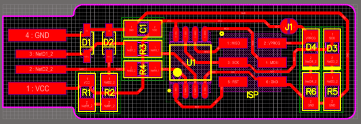
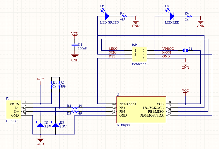
Below image is the brian schematic and board image:
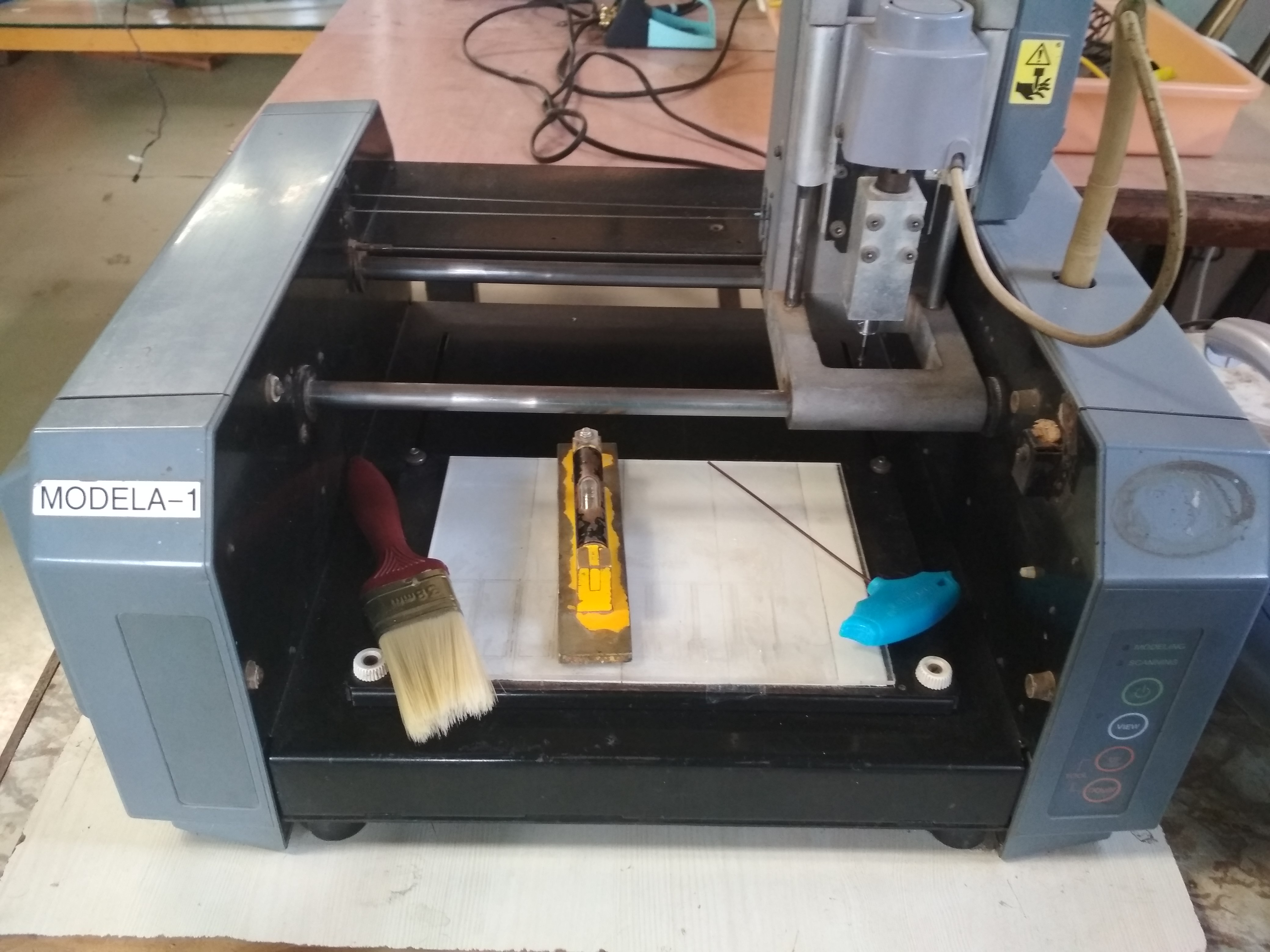
MODELA -
From here we started our work in group :
Introduction of machine
a. Bed area - 200*150mm
machine itself has 4 buttons:
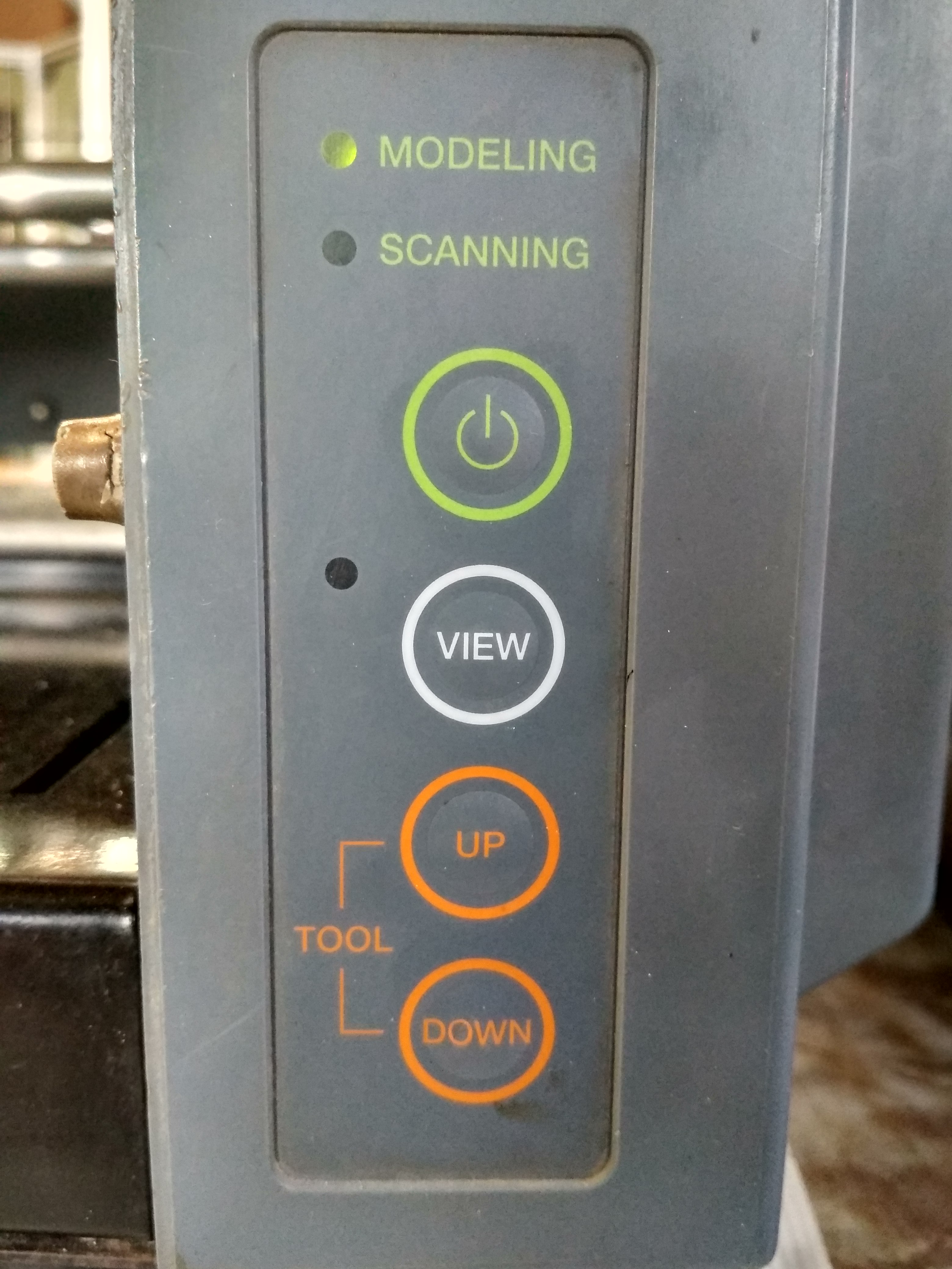
First button is used to ON/OFF the machine.
View - We can view our board between milling process.
UP - We can move tool (endmill in z-axis) in upward direction.
Down - We can move tool (endmill in z-axis) in downward direction.
Setting the machine for milling -
1. Bed Level -
we cut one acrylic sheet exactly same as bed area and stick on the bed area by using double-sided tape. Then we check the bed level by using levelling device.
2. Stick the board by using thin double sided tape on the bed.
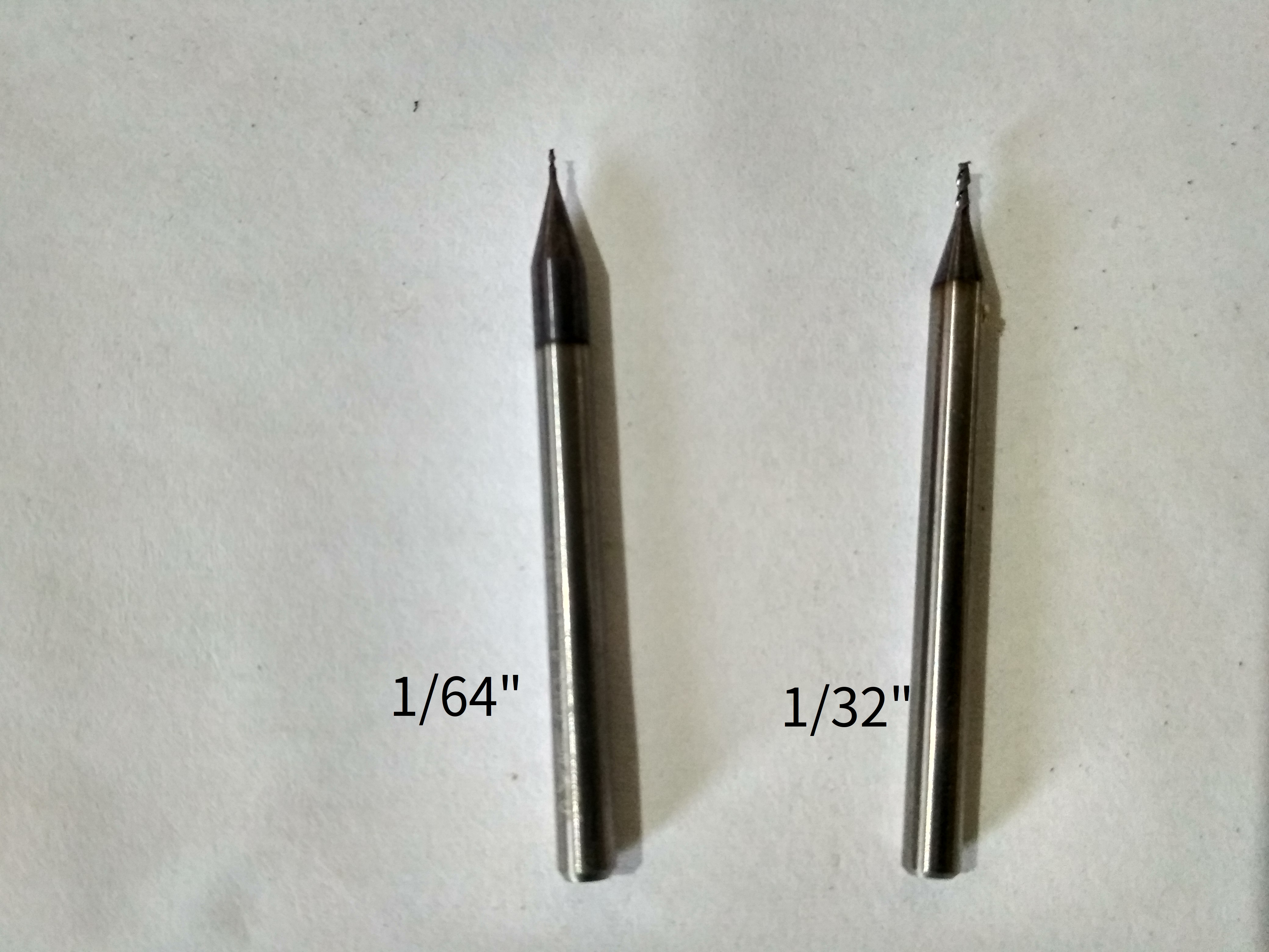
3. ENDMILL - 1/64" i.e. 0.4mm is used for traces the board and 1/32" i.e 0.8mm is used for cut the board.
We have to fix the end mill with the help of allen key.
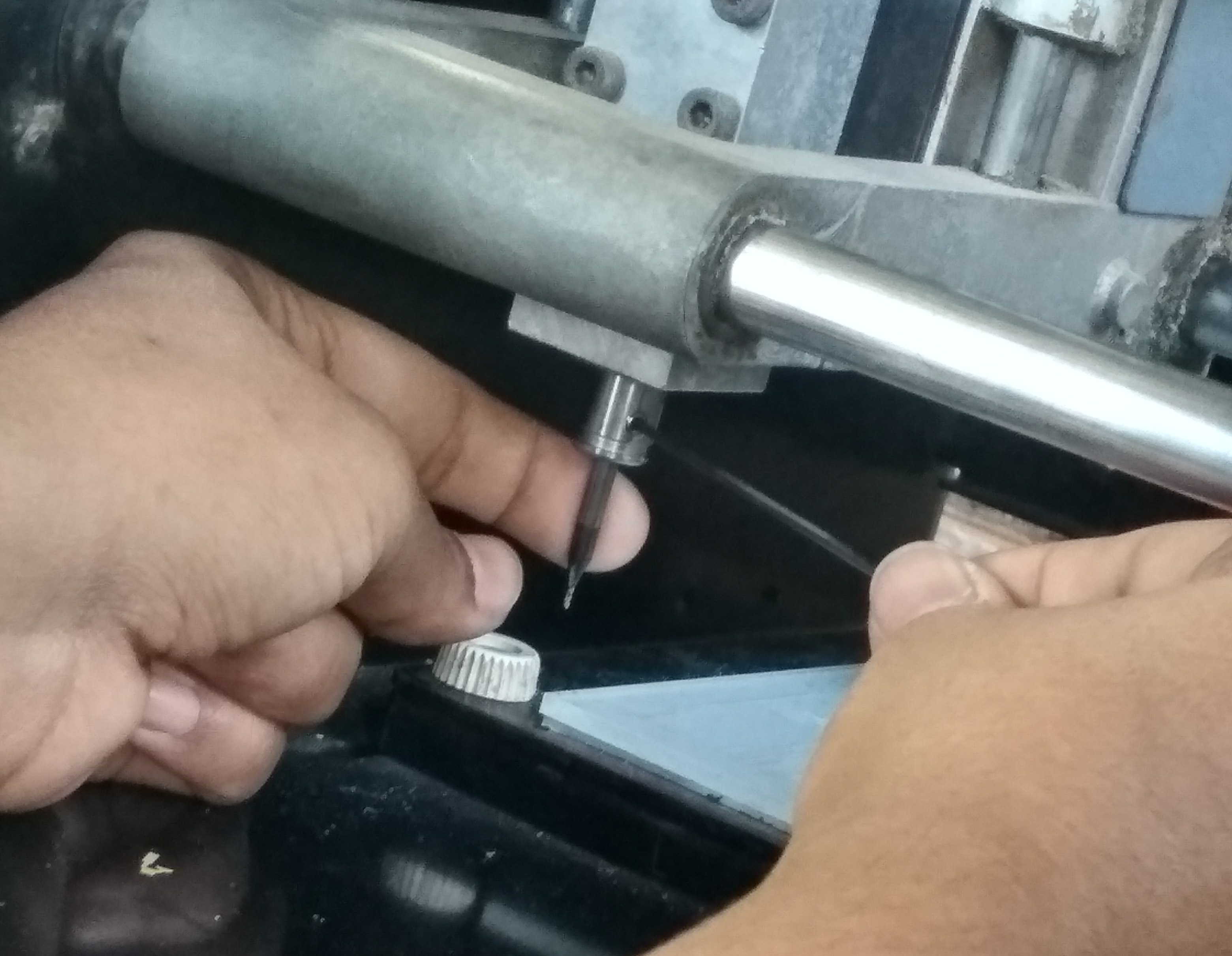
4. set the gravity -
We have to set the gravity because it results to break the endmills. For this, (press the DOWN button which is on the machine) slowly move the endmill header in down direction then loose the endmill and touch to bed by gravity and then tight it.
BY MAKING SETTINGS AND TAKING ALL THE PRECAUTION, BOARD IS READY TO MILL.
Now, we moved towards the computer/ software for milling.
I already downloaded the .png of the FABISP from brians document.
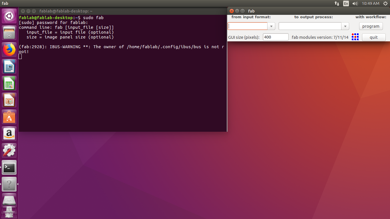
There are frequent network problems in Vigyan Ashram thus we are using offline version of Fabmodule.
Fabmodule :
1. Open the terminal and type "sudo fab" command. Then type the password.
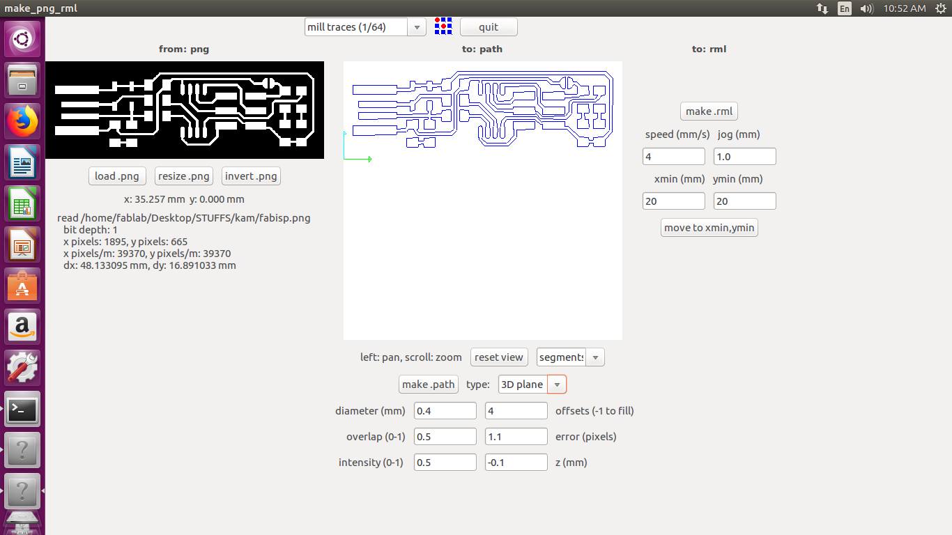
2. One new window opened in that we have to (make changes) set the image format, machine type which we are going to be used. Click on the "make_png_rml".
3. Another main window opened in which we have to load png and do some basic settings.
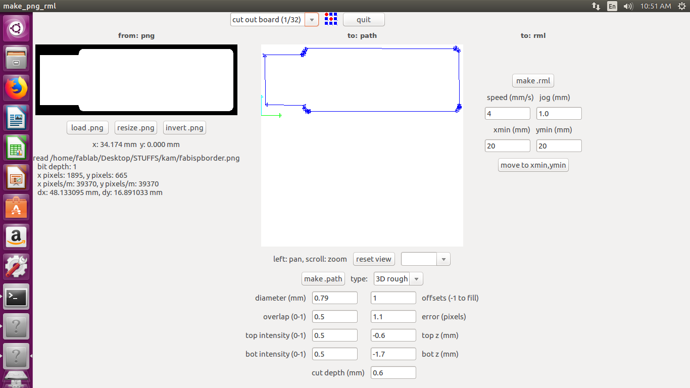
Endmill Selection - We have to select the endmill according to the process we want to do i.e if we want to make the traces we will select 1/64" endmill, if we want to cut the pcb we will select 1/32".
Offset - The number of turns of endmill for making trace/track. This setting majorely affects on the final product. Paths that are not cut in the first pass post probably will be cut during the other passes. So, more the offset cleaner the board and less the offset will have broad traces and very tricky to solder it. Also board looks dirty.
Z-axis - It is nothing but the depth setting. while tracing, How much deep endmill goes into board. If the depth is too much then it will be a reason for breaking the endmill. As per my instructor, I will keep the depth -0.06 to -0.1 for my PCB.
a. For traces we select 1/64" endmill and keep 4 offsets and -0.1mm depth settings.
b. For cut the board we select 1/32" endmill and keep 1 offsets.
check the bed level again just for conformation. Move the endmill to the origin and set the gravity.
All settings are done. Then go through following flow:
Click make .path - You should see the segments.
make .rml - The jog and speed set automatically, do not edit them.
Set xmin and ymin - Bit is placed on the board. Set the origin of the board.
I have spoil one PCB because of bad bed level or not setting the gravity correctly.
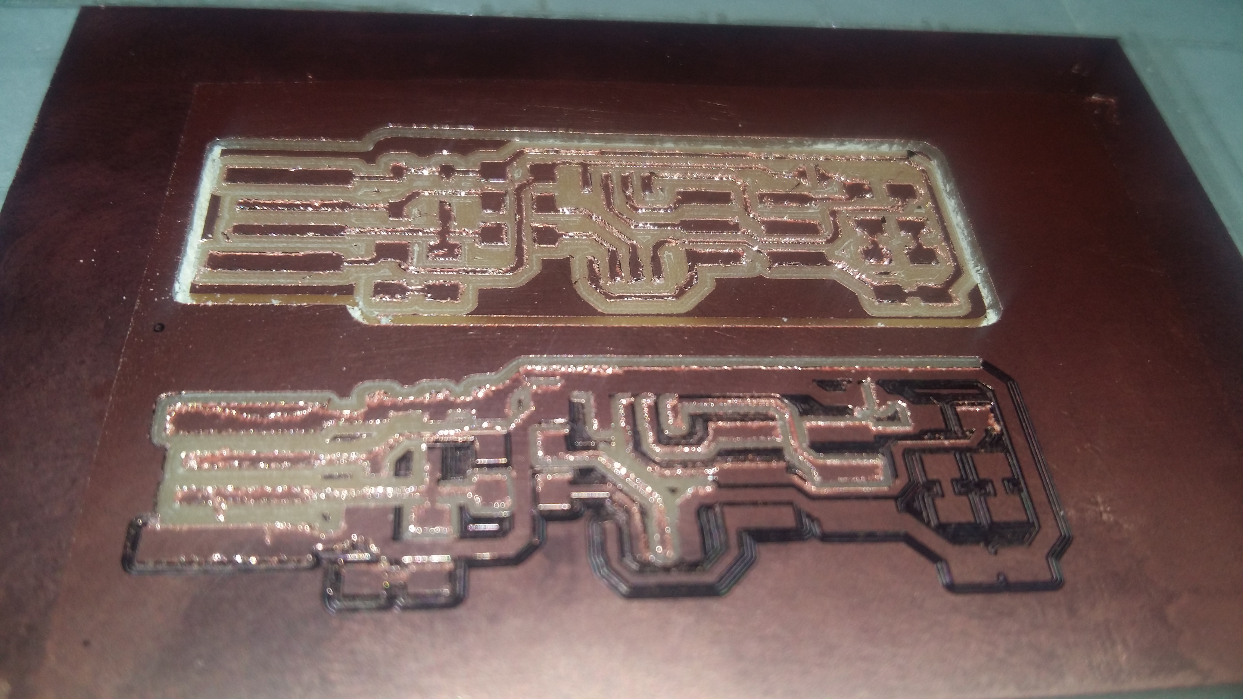
We try and use the PCB without any wastage.
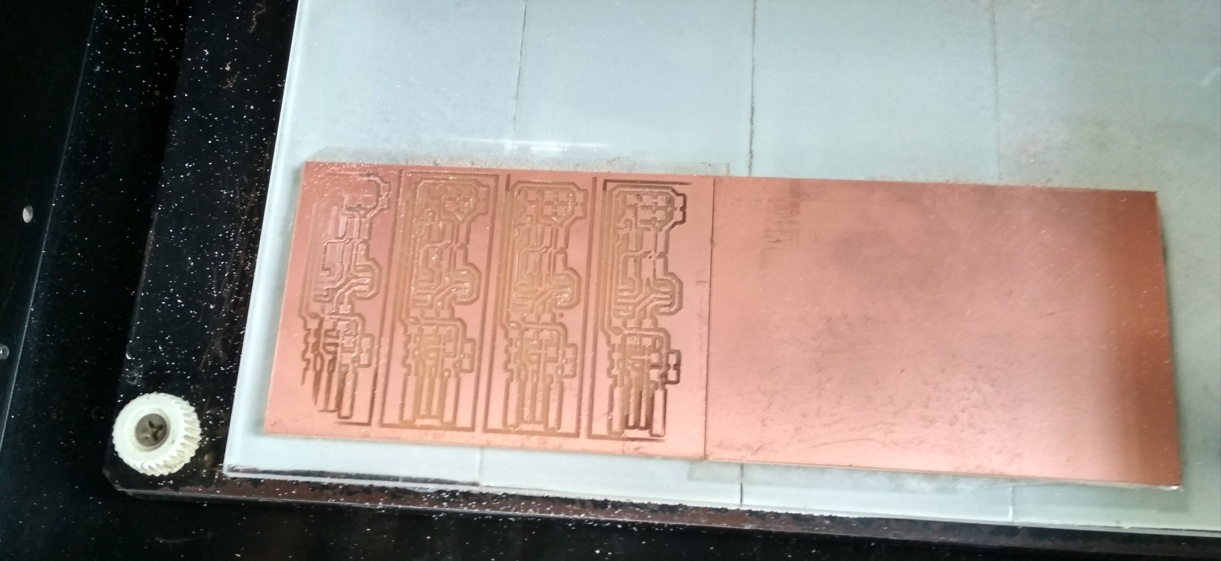
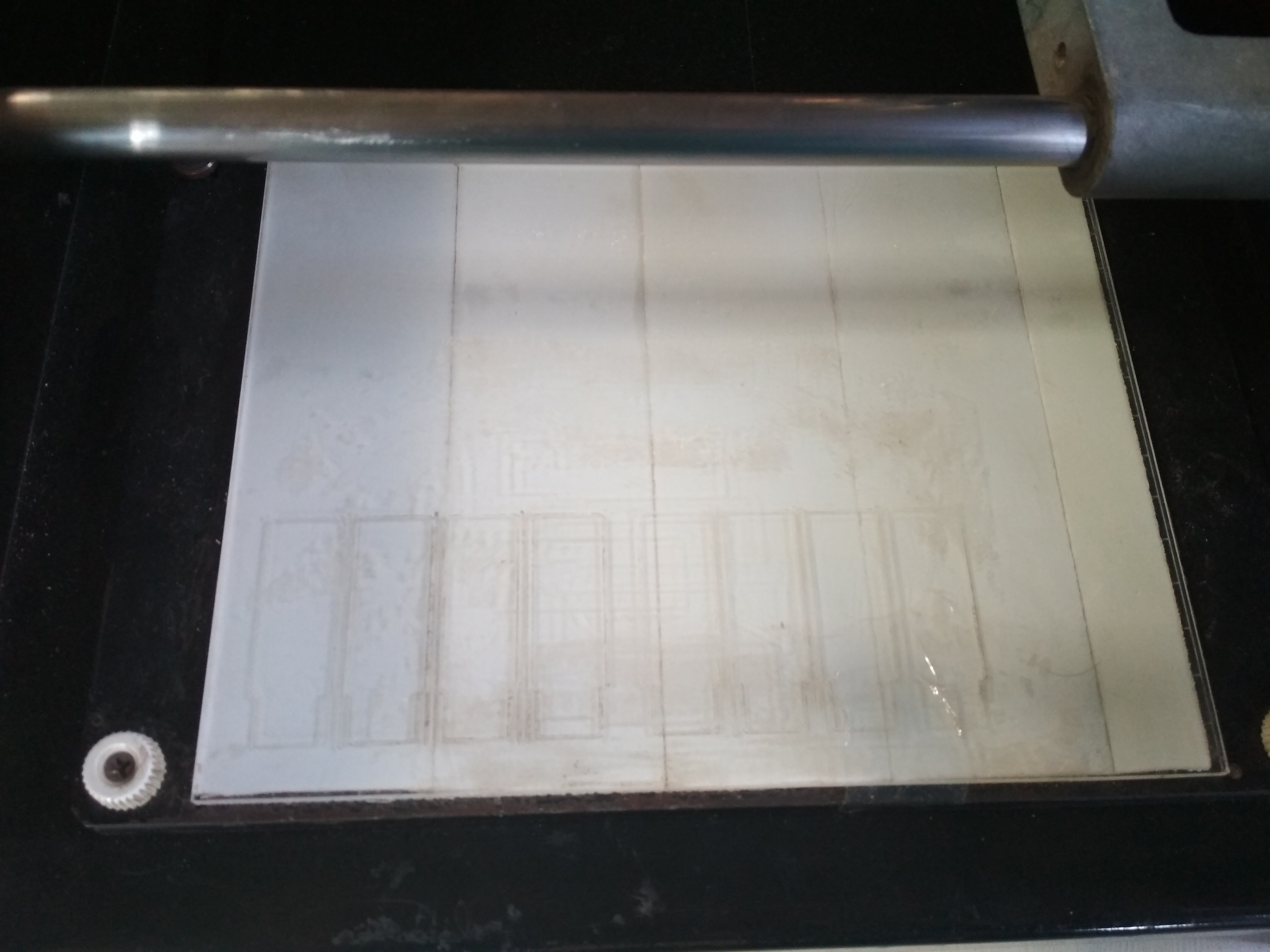
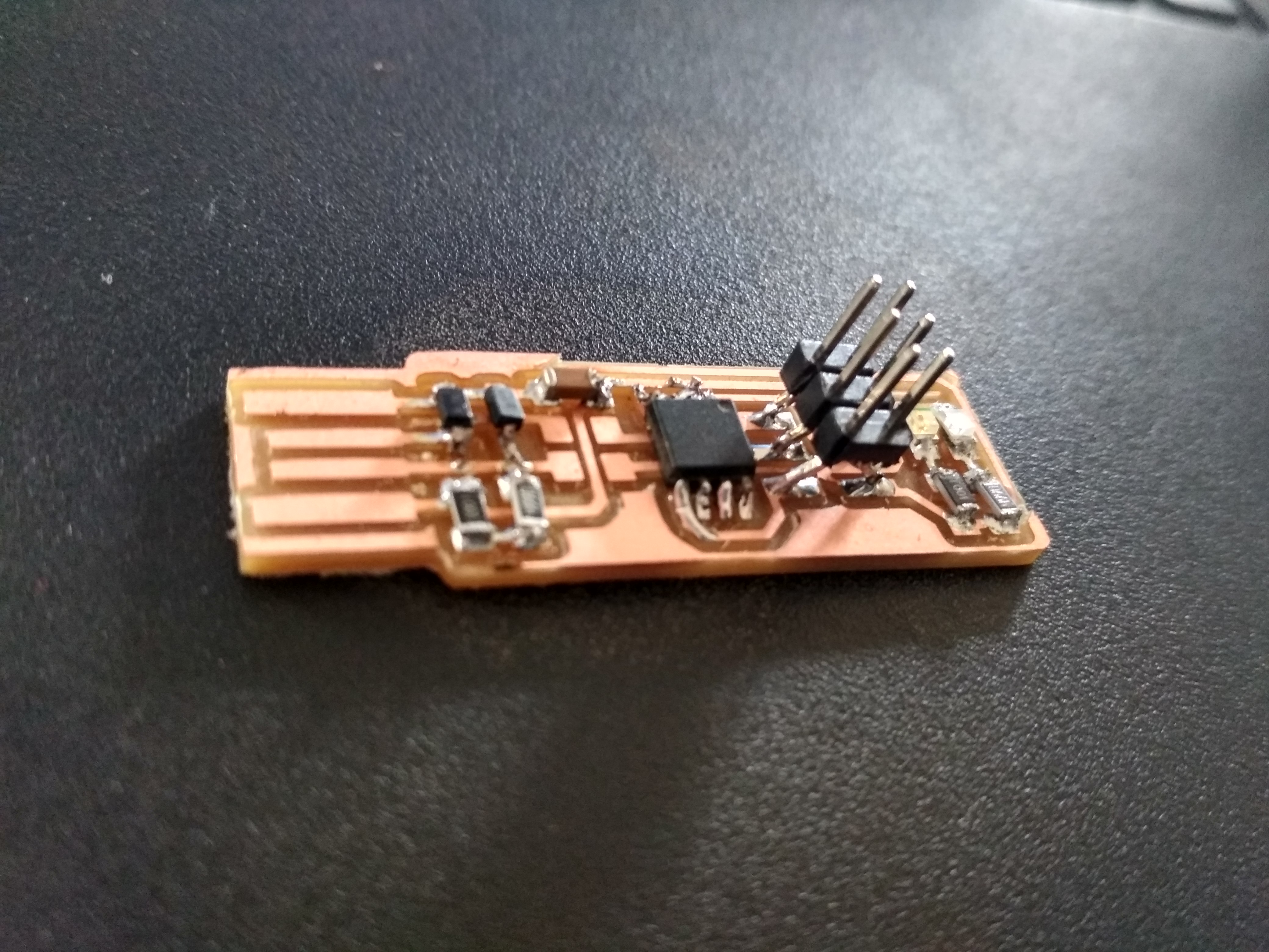
This is our milled brian borad.
Soldering -
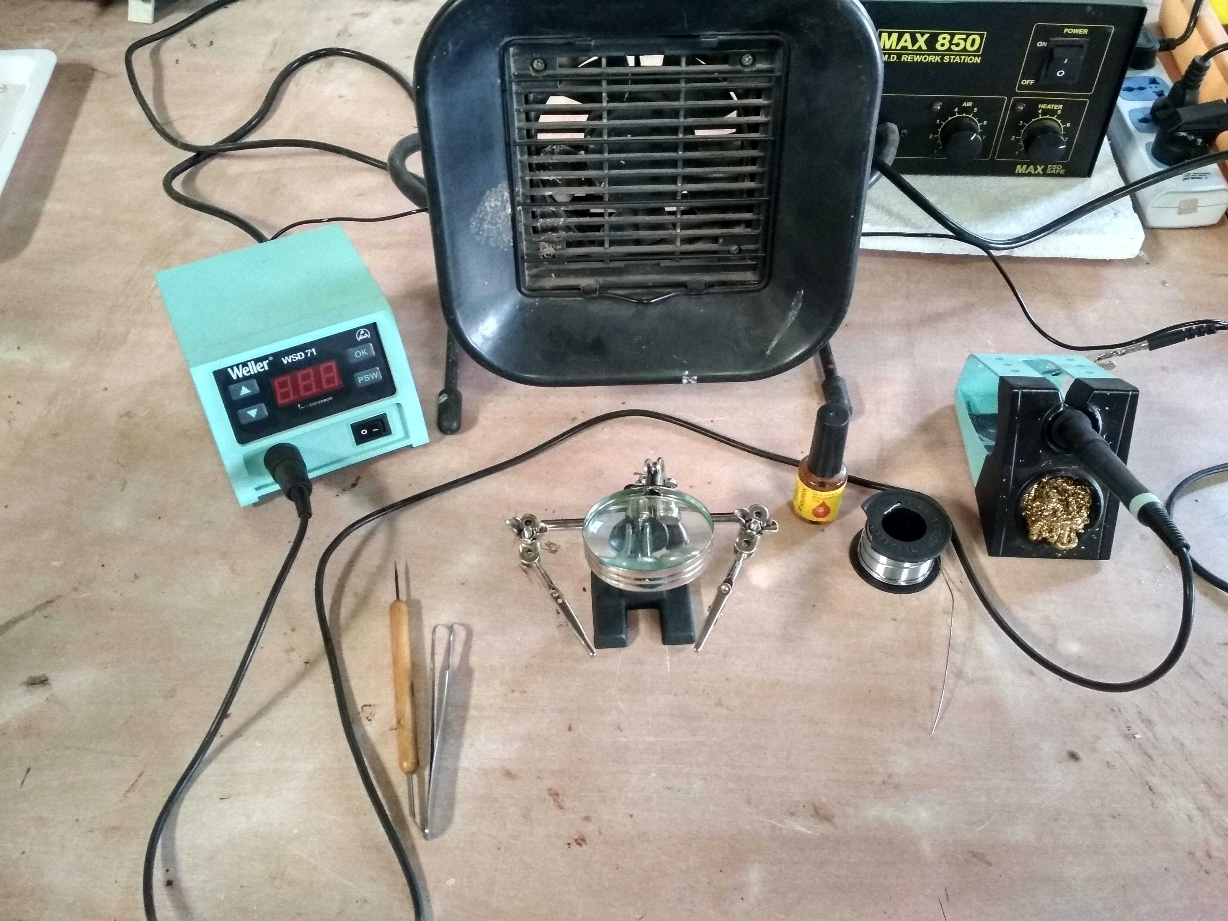
Before starting soldering we have to collect the components which require for brian board i.e. following:
- 1x ATtiny45 or ATtiny85 (I used the ATtiny45)
2x 1kΩ resistors
2x 499Ω resistors
2x 49Ω resistors
2x 3.3v zener diodes
1x red LED
1x green LED
1x 100nF capacitor
1x 2x3 pin header
I'm novice for this work that's why firstly I started soldering with wasted PCB. I'm trying to solder many components on track. I spend whole day for this with many mistakes like burn the track, improper soldering, wrong components,etc.
Then I took a good PCB and soldered it. But here I made one big mistake i.e I don't check the polarity of components especially the diodes, LEDs and orientation of IC. So I decided to make another board with good soldering.
I made new board. After stuffing the components I check it with the help of multimeter whether the Resister are showing the right values and there is connectivity or not.
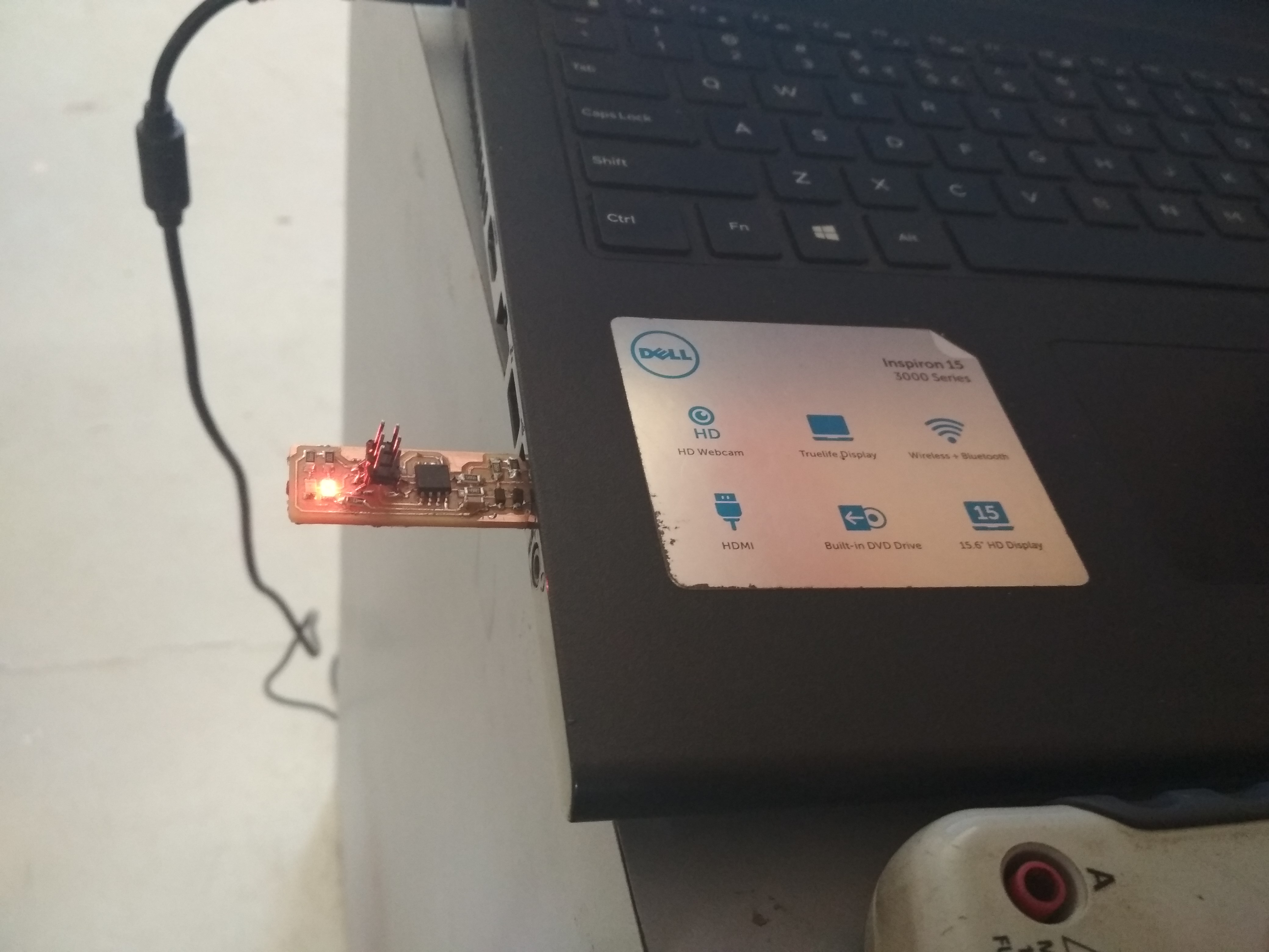
Programming -
I programmed my board using an asp programmer.
1. Connected my FABISP board to asp programmer.
2. just follow the below command:
sudo apt install avrdude gcc-avr avr-libc make
3. I downloded the firmware source code and extract the zip file. Open the terminal and go to extract folder.
4. Run make command. Now, I have file called fts_firmware.hex.
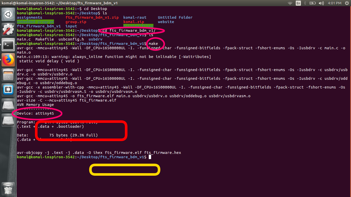
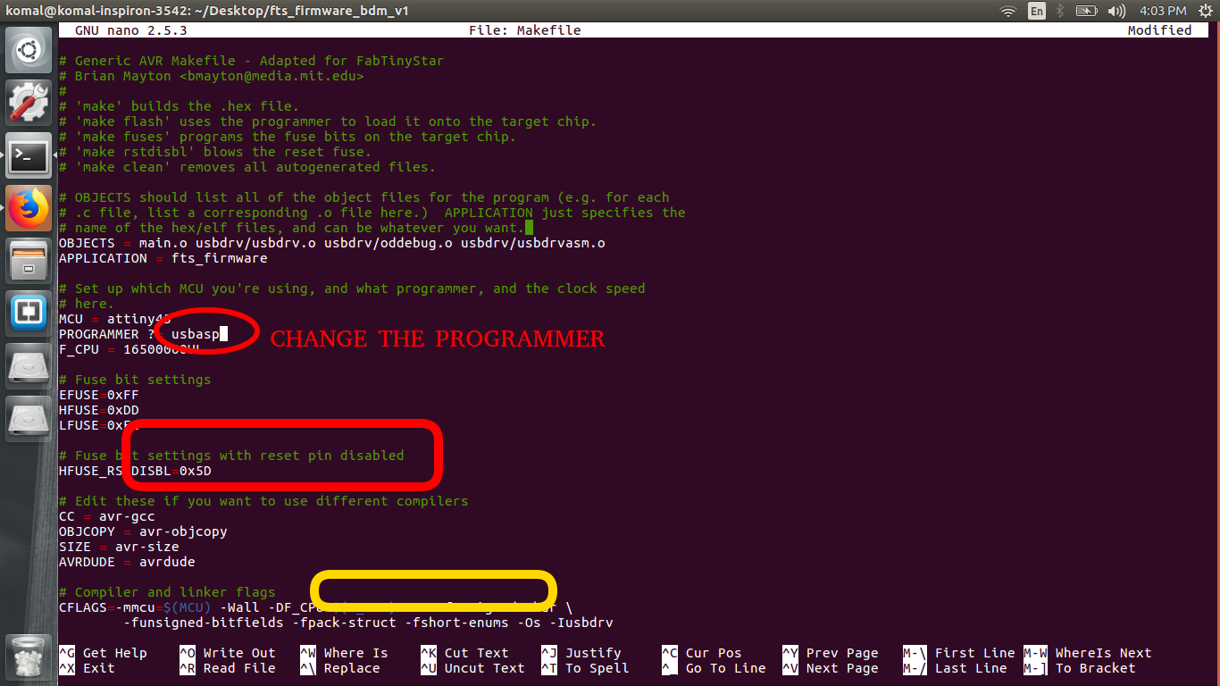
5. update the Makefile by using "nano Makefile" command for the type of programmer I'm going to use to program my board.
Edit:- programmer - usbasp
6. I Connected the programmer to the ISP header on board with correct orientation.
7. Run the "make flash" command. Here i got error.
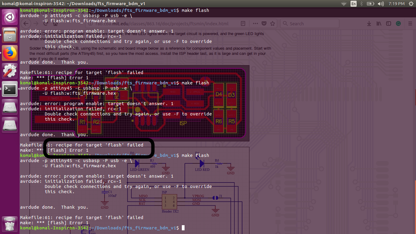
So, I check the programmer connect to the board or not, orientation of the Attiny45, etc. Everything is correct , I can't find the error. My instructor help me to find the error. He told me to check the soldering of components specially the Attiny45 and pin header and resolder them.
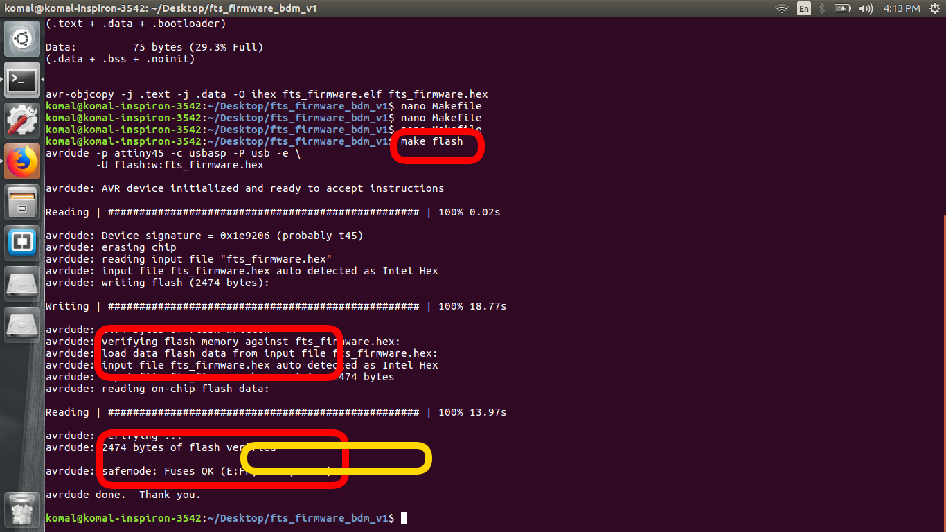
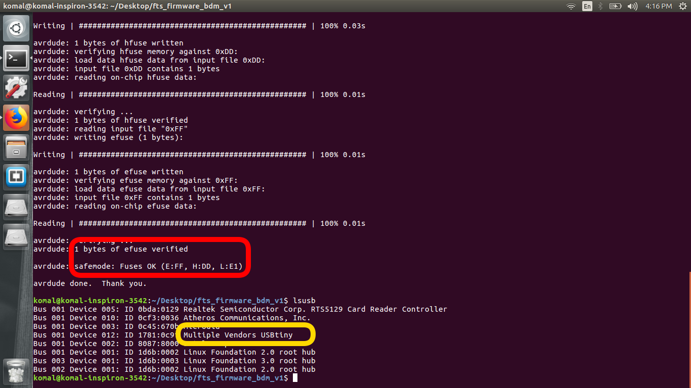
8. Again I run the command "make flash" and I have succesfully programmed the flash memory.
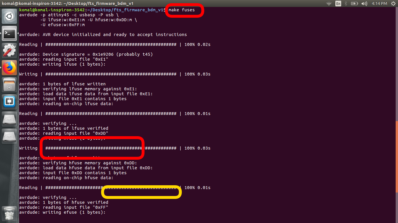
9. Run make fuses command. Done the programming.
After this just check that the USB is working on my board. Disconnect the programmer and unplugged board.
10. Type lsusb in terminal and can't see a "Multiple Vendors USBtiny" device.
So, I change my port and can see the "multiply vendors USBtiny"device.
Learning Outcomes
In this assignment I learned about PCB, milling, stuffing and programming. We learn modela and process of milling in a group. Soldering is a skill work and I have to improve my skill.