Back to Mejdi_FabAcademy_FollowUp
Final project chronicles
Gamma project: Blood_Analysis_from_BetaBioled_to_Gamma.pdf
A Portable, Super-accurate (ppm?), high speed (ms?) optical spectrometer with a BOM < 200 Euro. Measuring 8 to 16 wavelengths from the UV to the NIR.
From July 2017 to January 2018, on my spare time, I built a first working prototype: Gamma v6.
For my FabAcademy final-project, and sometime during the assignments, I will pursue the development and the documentation of this prototype.
NB: This page is structured as a log. A R&D Chronicle.
- My FabAcademy final-project, due by June the 18th, has been simplified to "just" the thermal-management & transportation box of the spectrometer.
- Complete build files and documentation of the Gamma Cool Box, as a independant open-harware project, is expected for Jully 2018.
- Complete build files and documentaion of Gamma v8 (pre-commertial spectrometer) will be made public, as part of a crowdfunding campain, in 2019 .
In the mean time: if one has the wish and the skills to help develope Gamma, please contact me! :)
- Build files of Gamma v6 will be shared through my FabAcademy repo in June 2018, but documentation will be very limited and version is still unstable.
February 2018
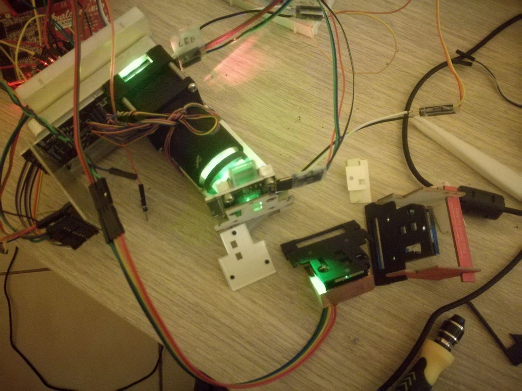
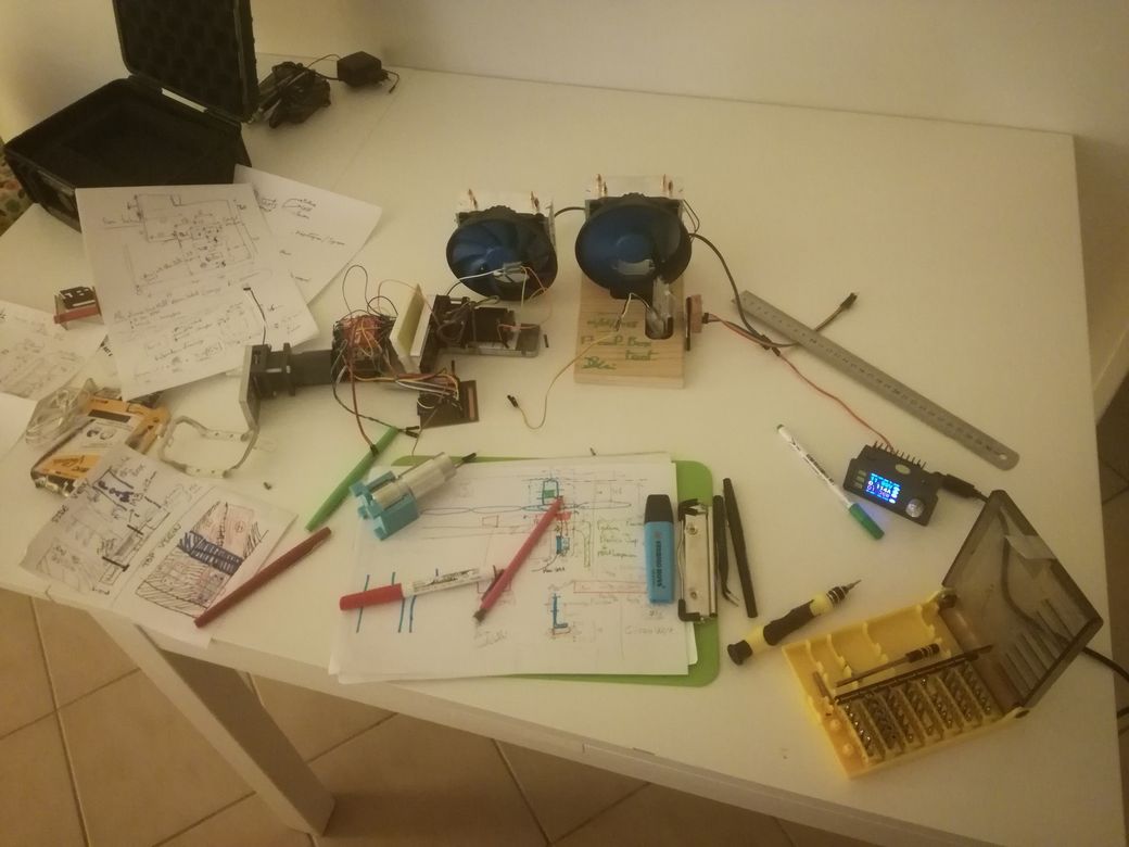
I started measuring blood with my Gamma v6 prototype.
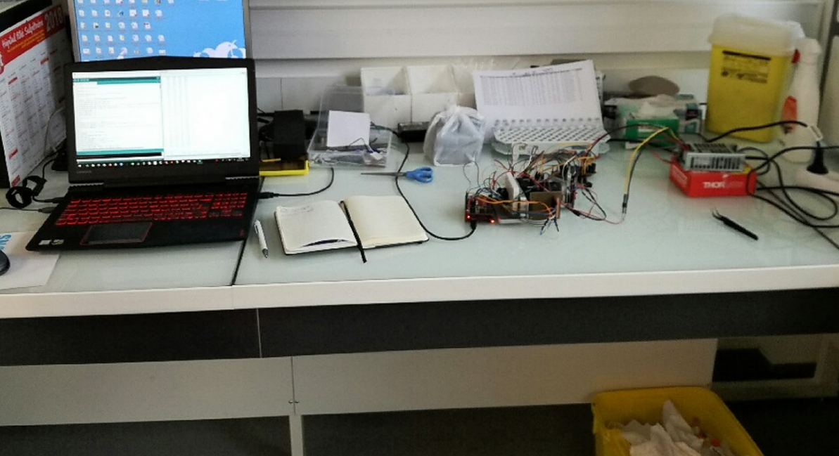
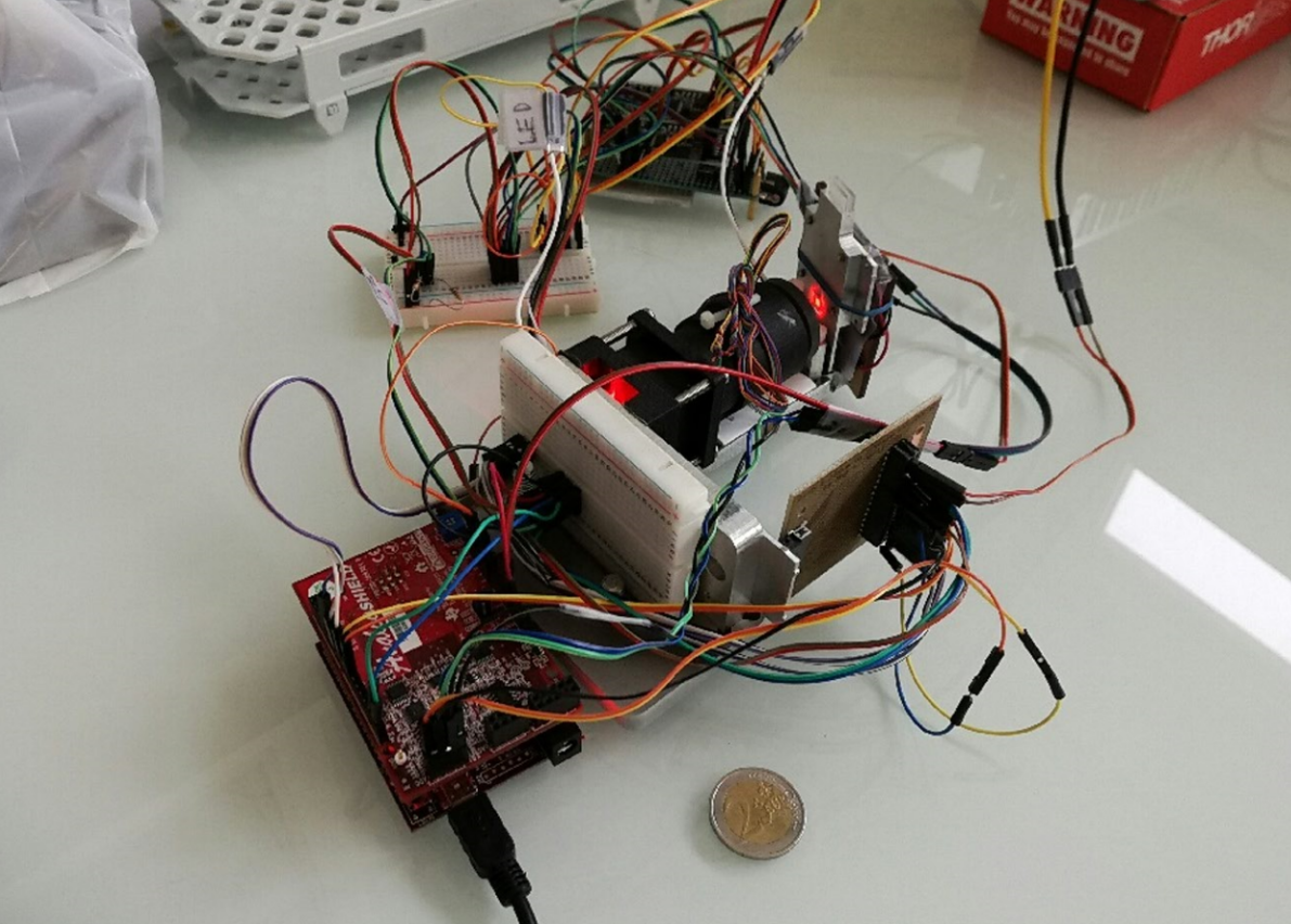
Unfortunatelly I ran into some issues with my photo-detector PCB. And while investigating them, I killed it -_-'
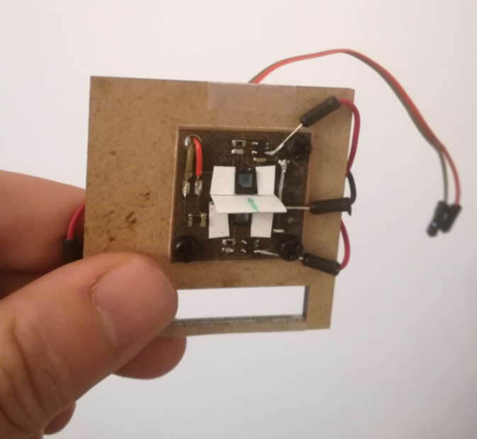
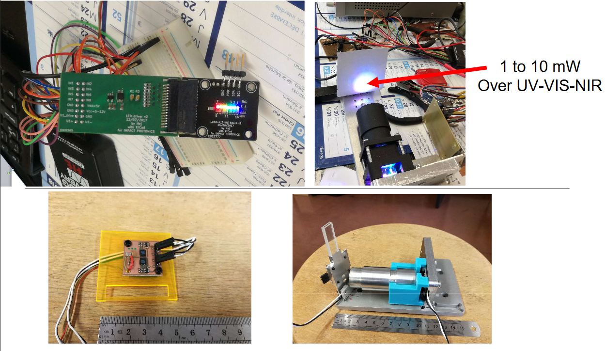
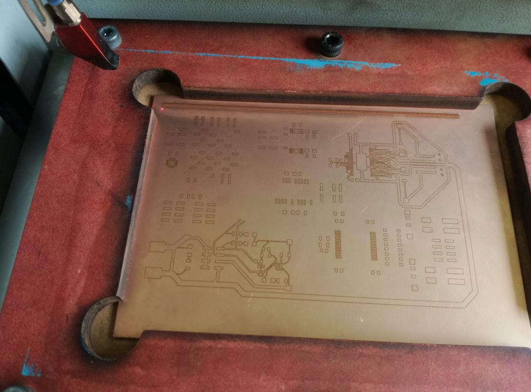
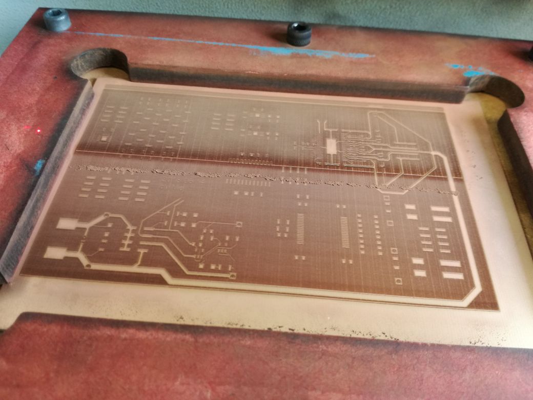
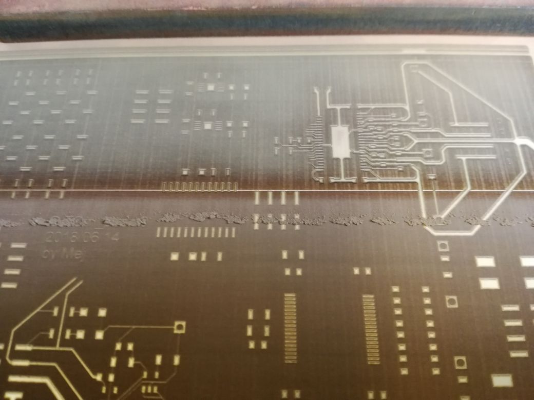
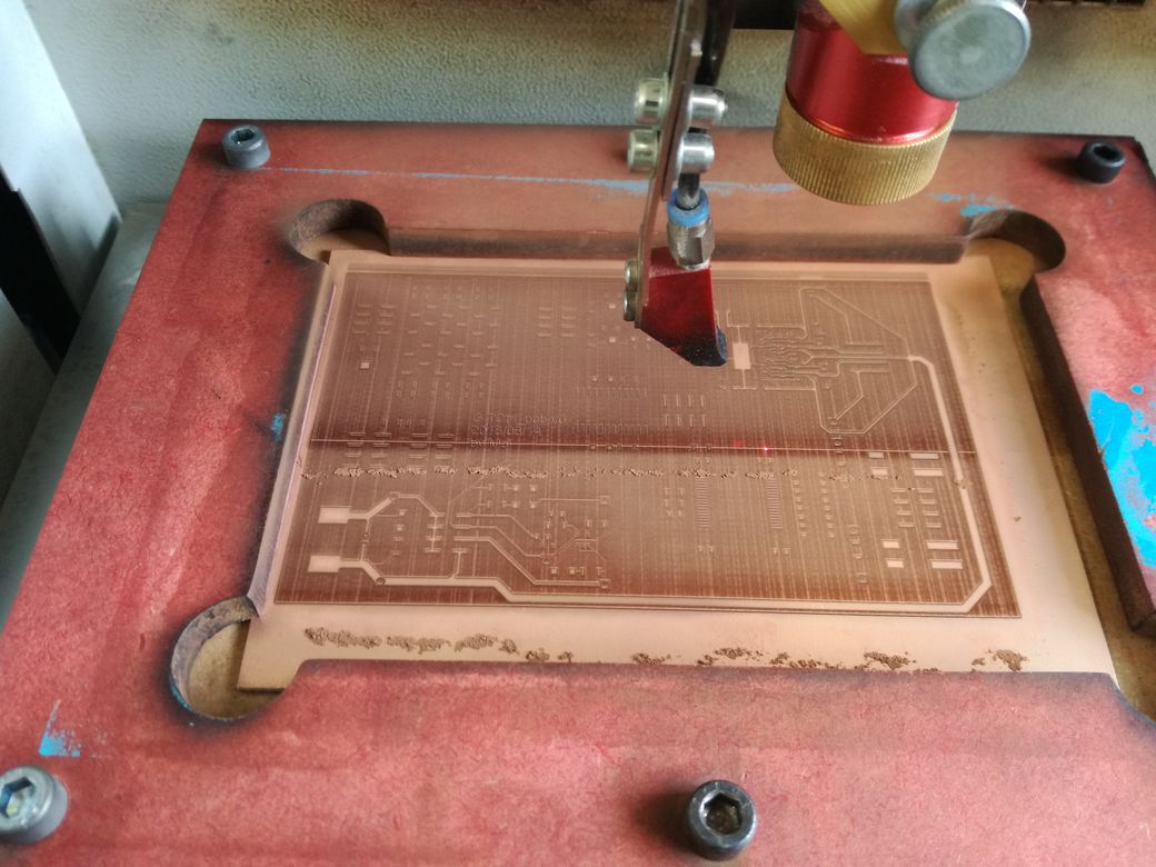
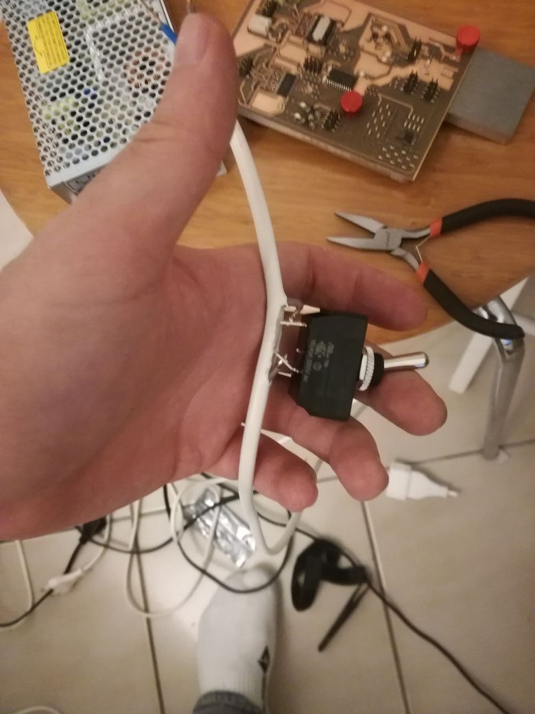
Making a photo-detection PCB
I needed to make a new photo-detector PCB. Possibly with 3 upgrades that I was postponning: Balanced detection + Connector on PCB's back + Tighter fit.
I used Kicad to draw the PCB shematic and root it.
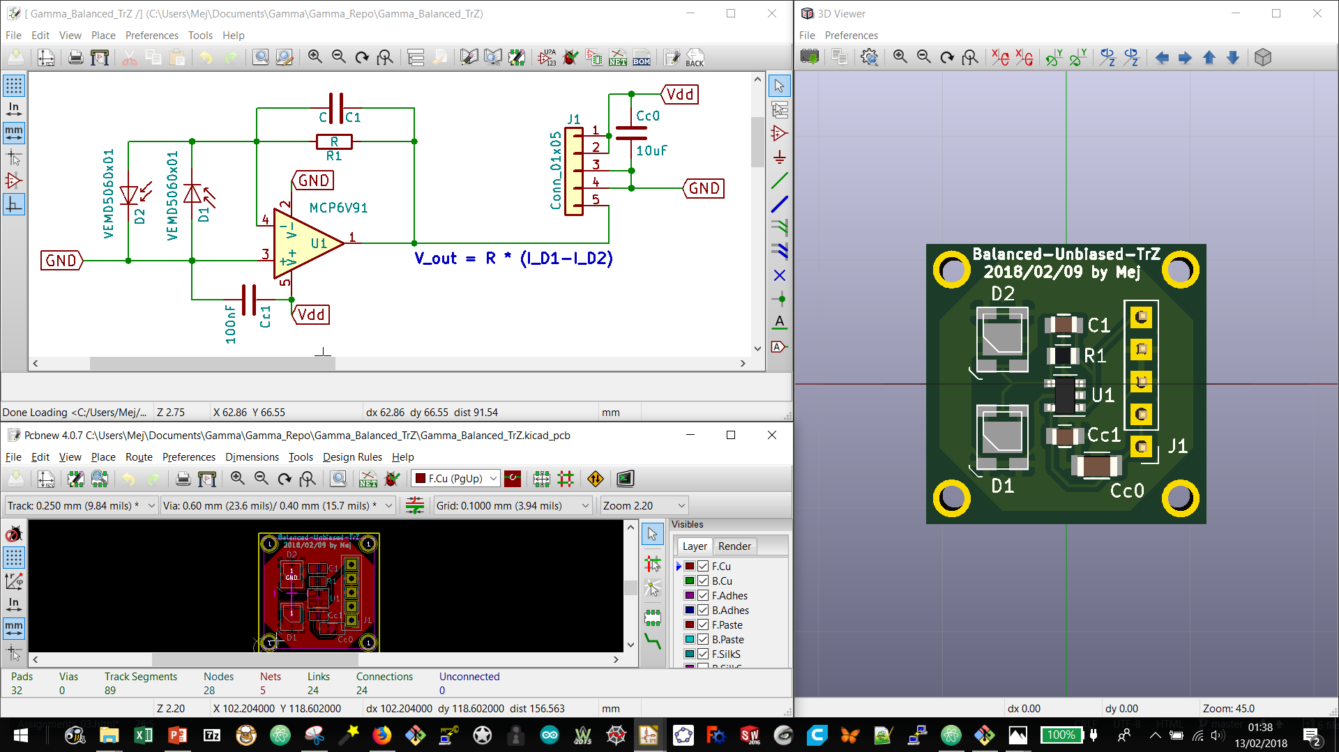
In my Electronics Production assignment I used this PCB to document my PCB production workflow
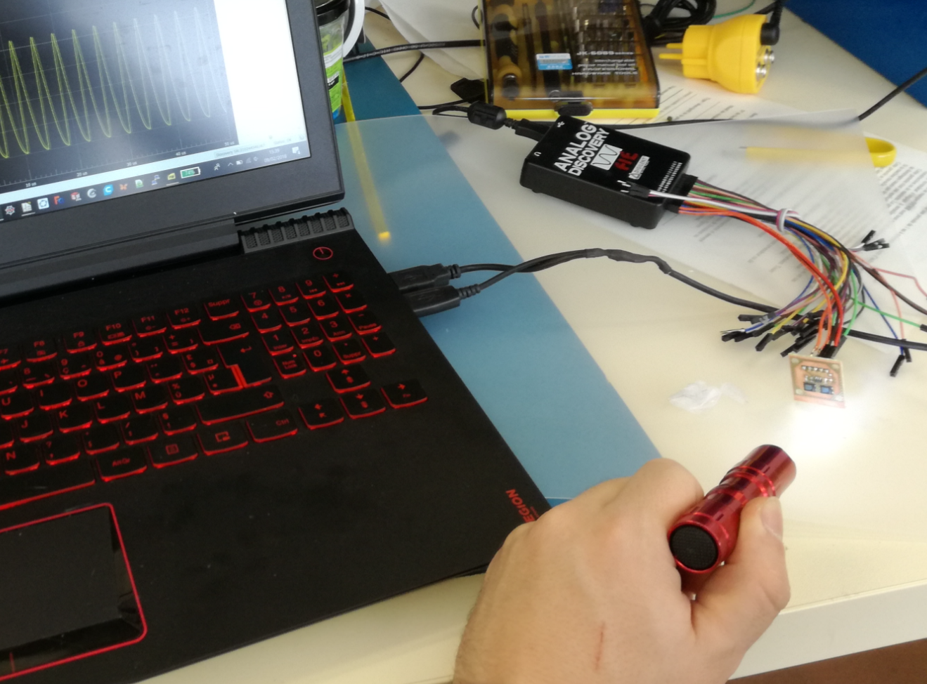
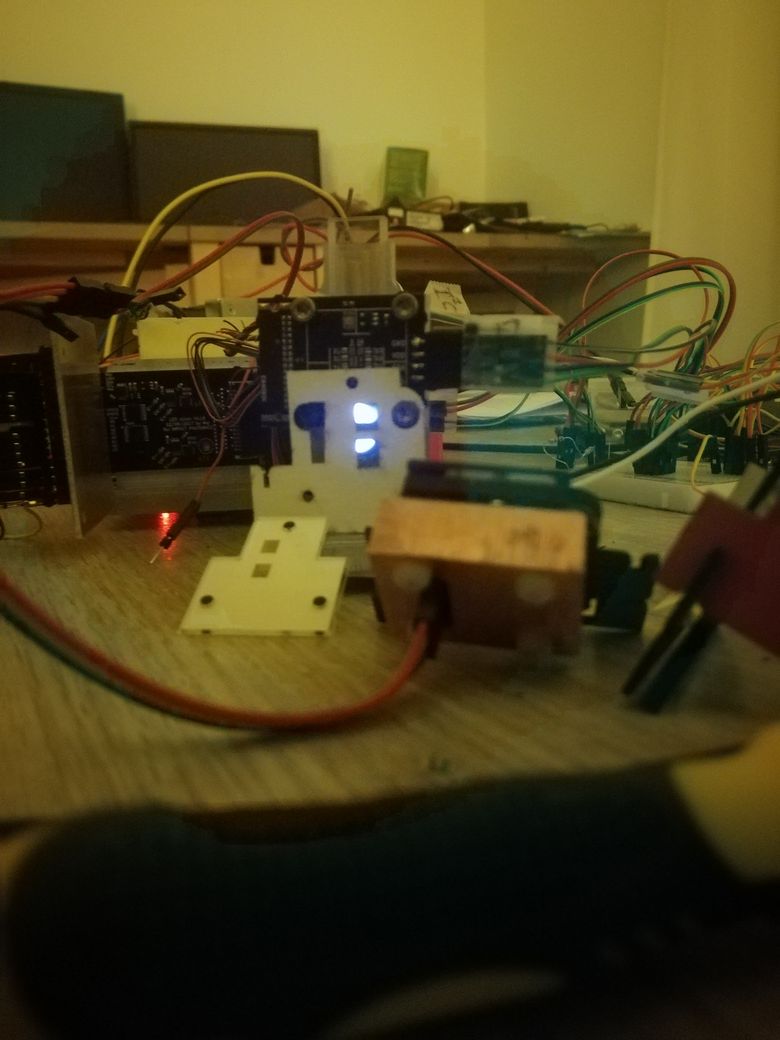
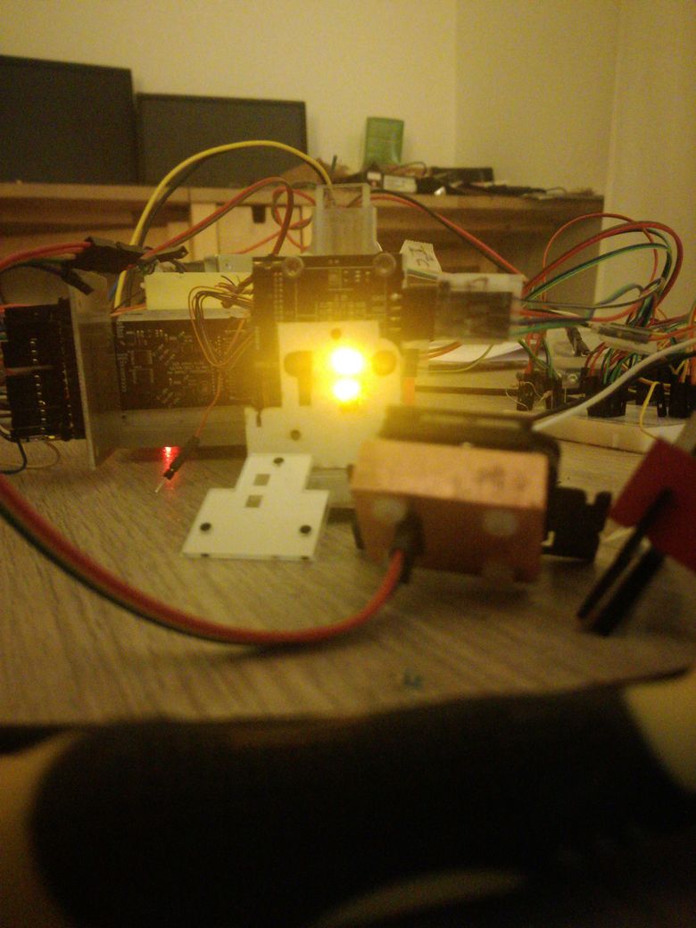
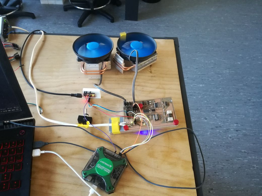
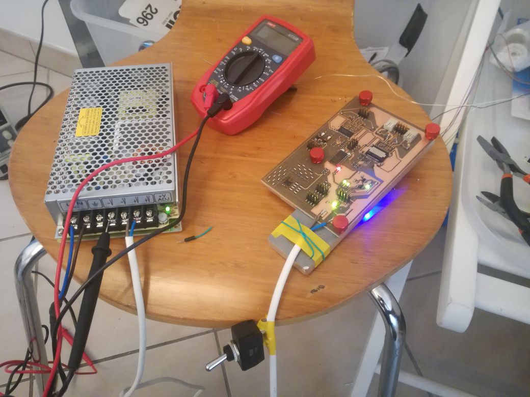
I tested the PCB using an USB Osciloscope (Analog Discovery 2). I just need to align it now...
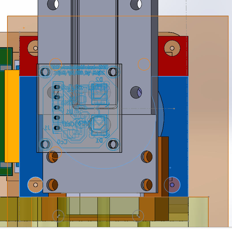
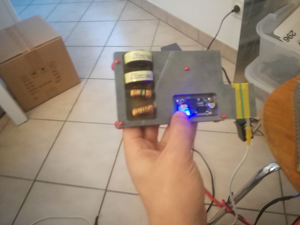
Making the PCB holder
Using my "Cut and fit" assignement I did a window and holder for the PCB. Details here
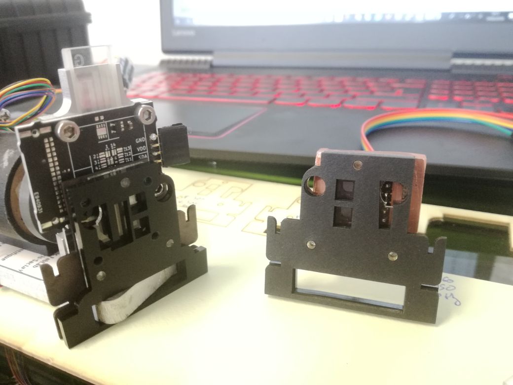
And here it is on the field, ready to be mounted on Gamma:
March 2018
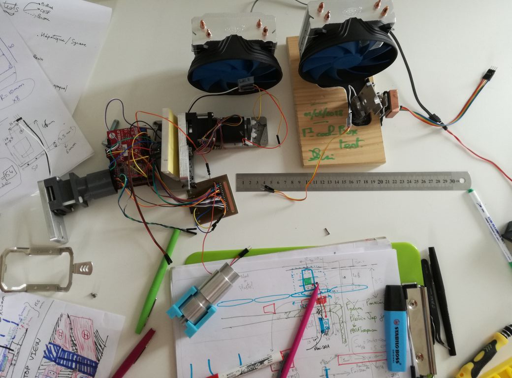
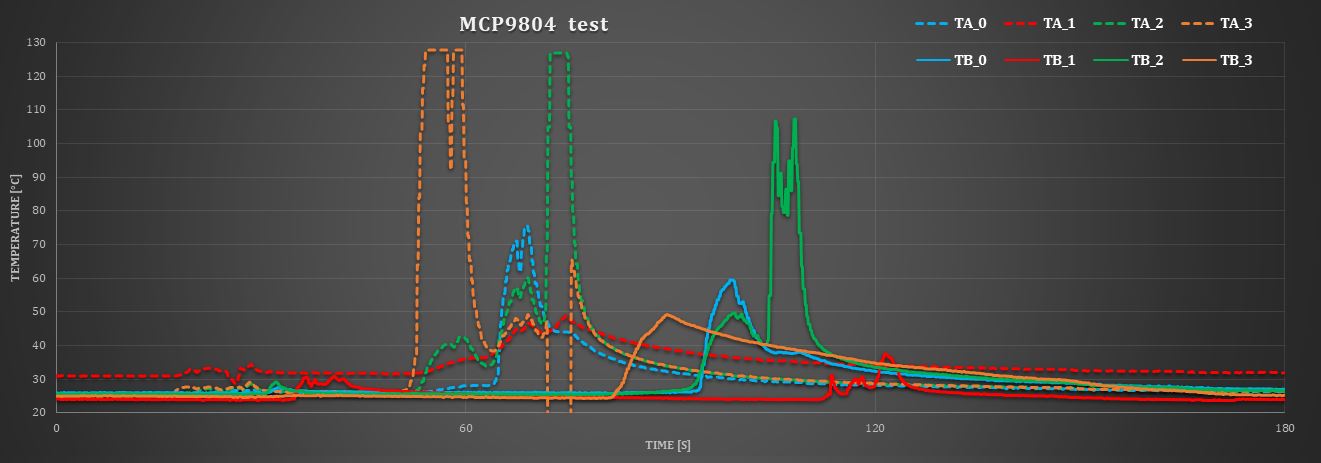
I did a second run of measurments at the hospital. I studied the serum of patients with more or less advanced liver disease.
I especially studied the drift of the absorption with respect to the serum temperature (over the range 5 to 35°C).
Results were encouraging, but I need to reduce the thermal cross-talk between the different elements of my spectrometer.
Indeed while the temperature of my sample oscilate between 5 to 35°C (with a 1st peltier module) and that I thermalise my LEDs @ 20°C (with a 2nd peltier module),
I need my Photodiodes and my electronics (especially the ADC) to remain at constant temperature. With deviation of less than 1°C.
I could cut the spectrometer in differents blocks, separated by 5 to 10mm each:
- The LEDs driver PCB, which needs to dissipate about 10 Watts
- The LEDs PCB & its peltier
- The cuvette holder & its peltier
- The Photodiodes PCB, which is very close from the cuvette holder
I could then attach those blocks on independant radiators (ie Aluminium base plates), press-fitted into an insulator (eg a wood plate).
I would
just have to be able to control the temperature of the radiator plates...
Also, since such a set-up would have to be distributed all around the spectrometer, it could be a good opportunity to integrate it as a transportation box.
My FabAcademy Final-Project is to make, using only FabLab materials and DIY tricks, a
multi thermal control and
transportation box. Connected, of course.
The box will be designed for my spectrometer, but could also be used/addapted for other kind of scientific instrumentations projects where thermal management is critical.
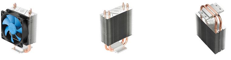
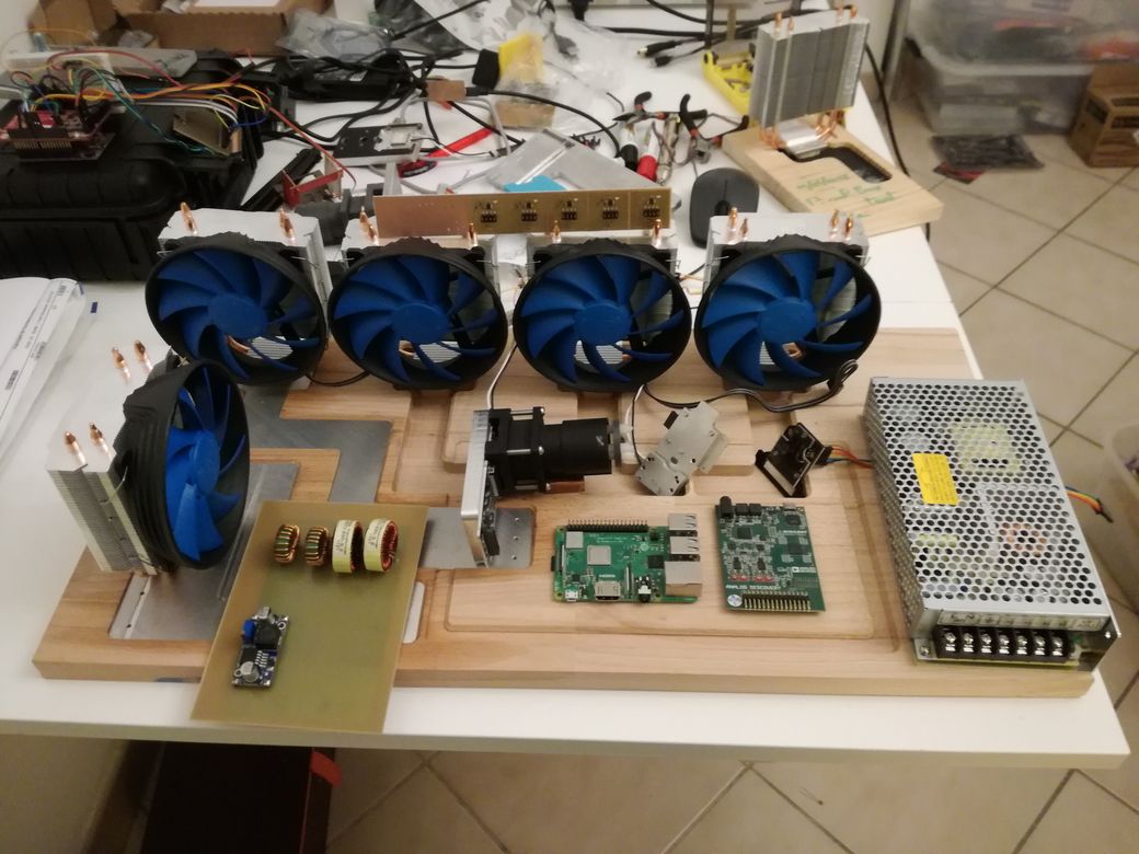
For the thermal dissipation, I will use CPU fan cooling-systems. As they are mass-produced, there are very affordable.
I chose the
GAMMAXX 200 of
Deepcool.
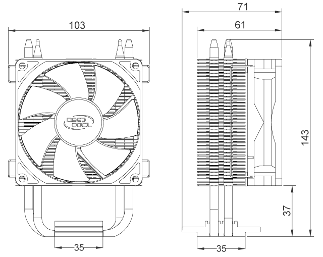
Key specs:
- Easily available online for 12€/unit.
- 12V, 200mA
- 1000 to 2000 RPM, 30dB noise max
- 42 CFM (feet3/min) = 20 L/s
- 95W dissipation
Use the CPU fan
4 pins connector standard:
- GND
- Vcc: 12V DC, 13.2 max
- Speed sense: 2 pulses/rotation
- PWM control: 25kHz (+/-3kHz), 5V max, 0.8V HIGH/LOW threshold, duty-cycle tunes fan speed
May 2018
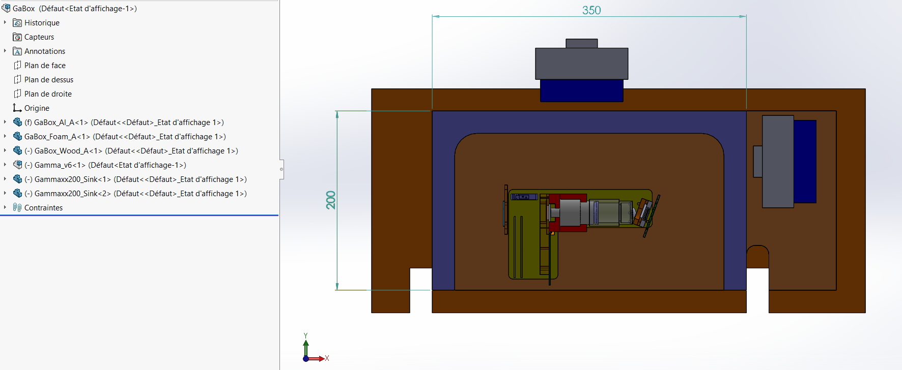
General sketch of the Gamma Cool box
Choice of a RF communication solution
In the
Embedded programming assignement I evaluated the nRF52 MCU familly. No go. Nordic is not Fablab friendly.
For now I will use Atmel AVR MCU, only. Whith USB linking through Arduino or Eclipse IDE.
If time, could add an external RF IC through I2C or SPI, like this
one.
General Bill Of Material
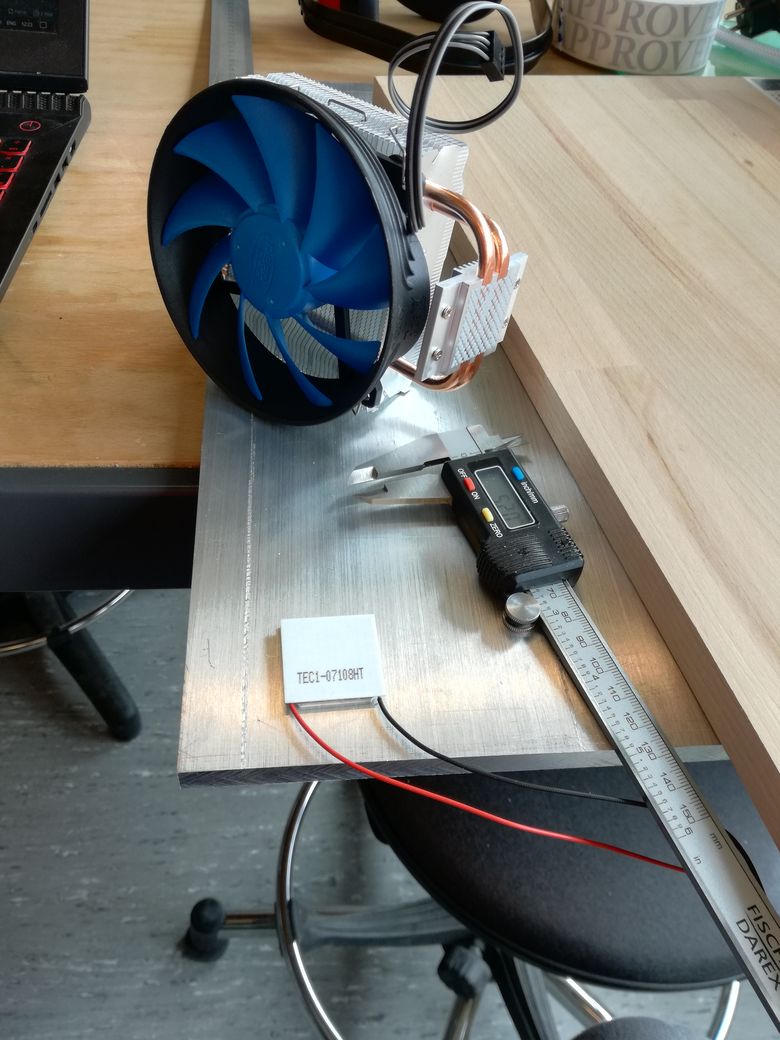
For the peltier, Ill use the
TEC1-07108HT:
- 5€
- 30x30x3.5mm
- 8.5V/8.5A max (70W)
- 0.9 Ohm => P_joules=65W at Imax
- Q = 40W at ΔT =0°C
- ΔT max = 68°C (Tmax=225°C)
For the peltier driver, I'll use a high-current DC motor driver + a low-pass LC filter in order to smooth the current.
Maybe the
DRV84x2 of
TI:
- Dual bridge (ie: 2 channels)
- PWM controle. I would have prefer I2C, like the DRV8830, but ha.
- Fault and auto-shutdown: Over Temperature, Over/Under current
- 3A/channel for DRV8412 (6A peak) @ 3.4$/unit by 1k - 6.6€ in retail
- 7A/channel for DRV8432 (12A peak) @ 6$/unit by 1k - 12€ in retail. Few suplier have it in stock...
- CBC (Cycle by Cycle) current limit
- GND to PVDD operation! Rare for high-current bridges (usually 2 or 5V to PVDD), but versatil: allows low impedance loads.
Why use LC filter and not RC filter? Why a low-pass filter at all?
I've read a lot of obscure explaination on the internet. Here is the simple truth:
DC motors behave like big inductances. They would smooth any PWM.
Peltier behaves like a simple resitor. When the driving current of a peltier is turned off (eg in the low of a PWM), the heat flows from the hot side back to the cold side.
We lose the ΔT of the peltier. It's inefficiant. Ergo the filtering.
Since resistance means joules losses, especially at 8A, we don't use resistors in the filter.
Shielded Inductance with L>0.3mH and I_max>5A? 9 options on
mousser...
Since cut-off frequency will be limited to ~1kHz, it would be great to have "high frequency" PWM. Meaning 20kHz or above.
June 2018
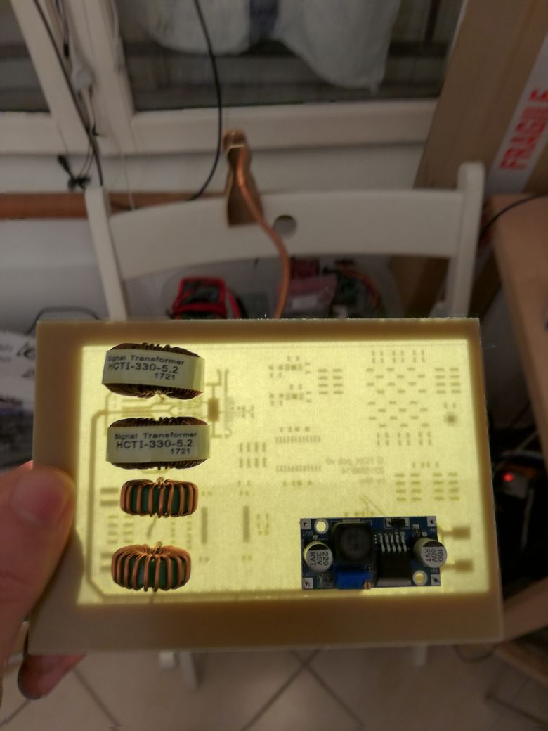
Updated BOM is available in xlsx and pdf.
See also my Applications and implications assignment for insights on the BOM.
Many ICs are used for this project. Here is a R&D memorandum I did to have quick acces to their key specs.
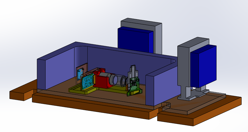
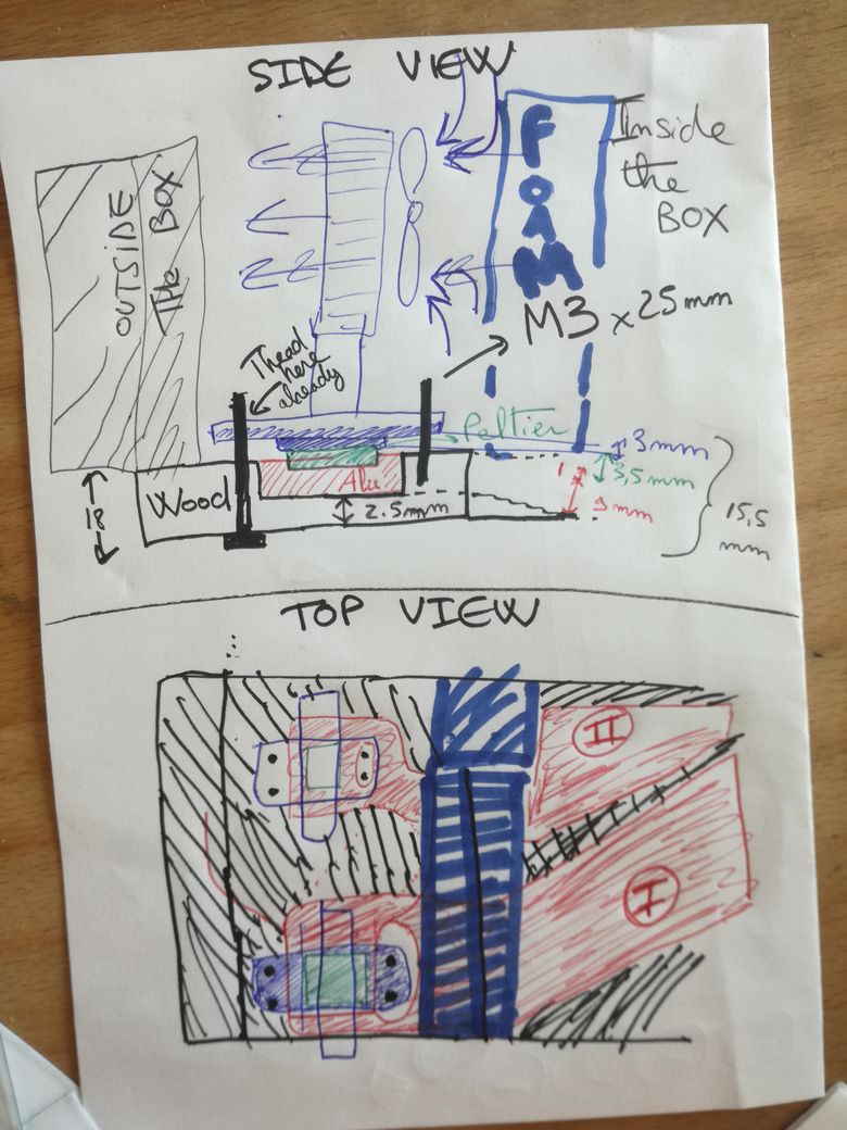
Mecanical design
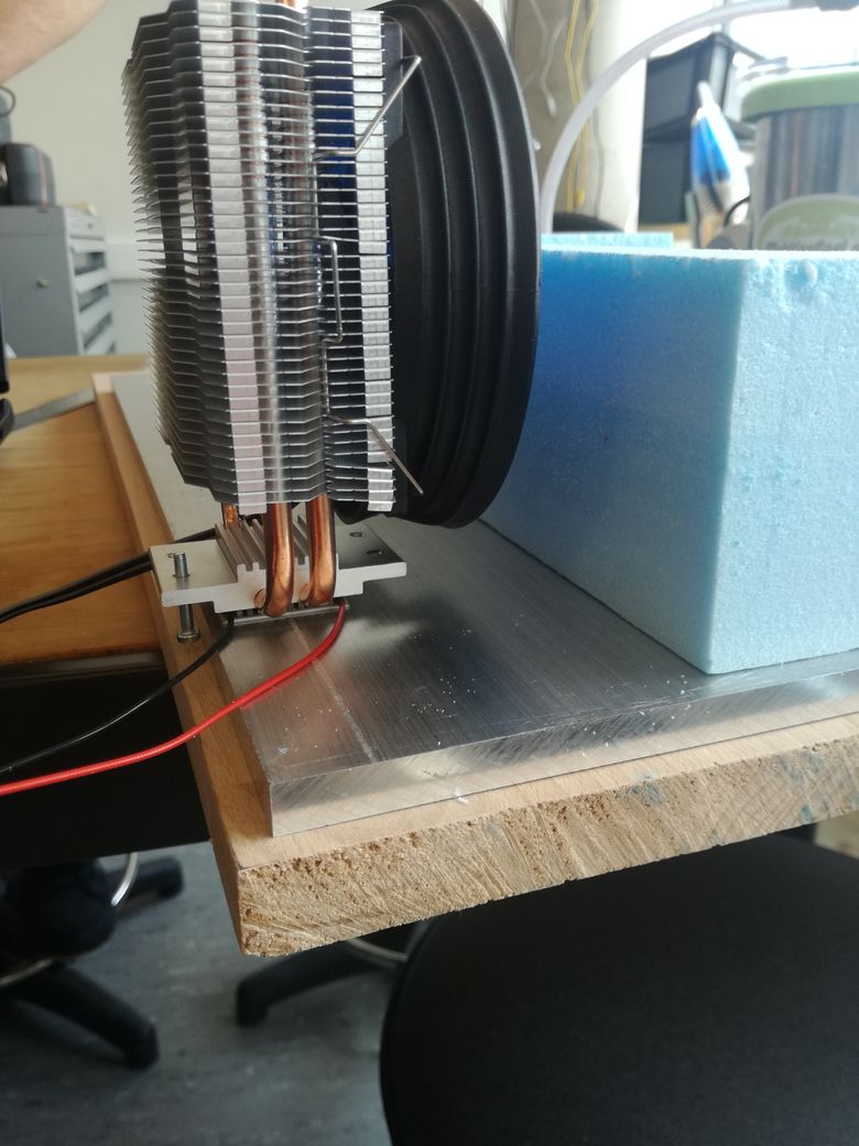
For my
wildweek assignement, I worked on a single "thermal line" of the
Gamma Cool Box.
I found a simple way to assemble the wood, the aluminium, the peltier and the fan.
With this sub-assembly validated, I could then sketch the complete box.
NB: 10mm aluminium may be too much. It takes a long time to cool or warm (0.02°C/s). Could be changed for 8 or 5mm.
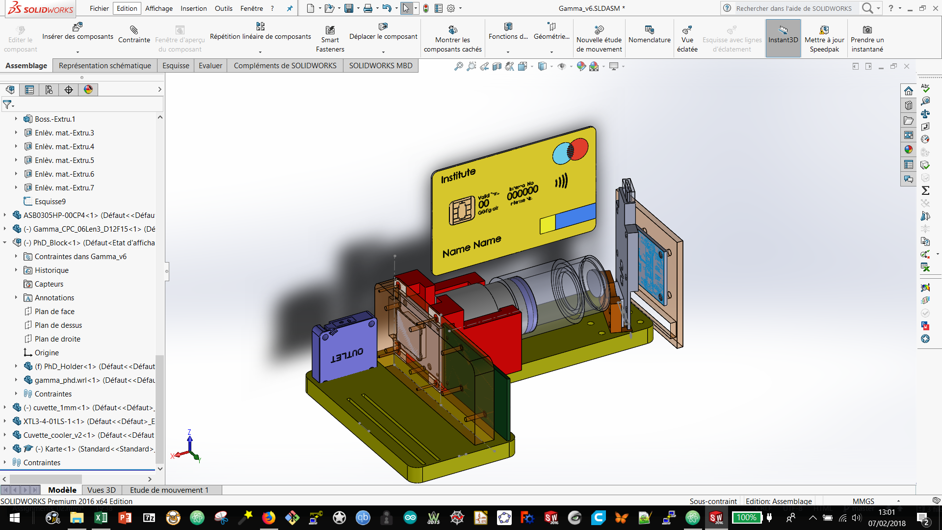
Using Solidworks I adapted the design to my
Gamma spectrometer.
I added a 5th fan and aluminium pipe (on the bottom left). I will use it to cool the main PCB.
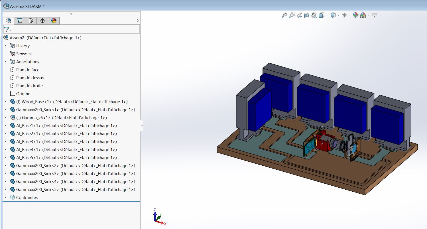
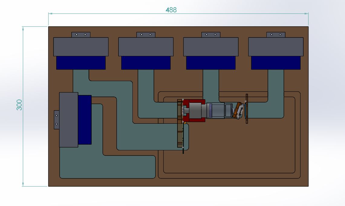
Source files available
here.
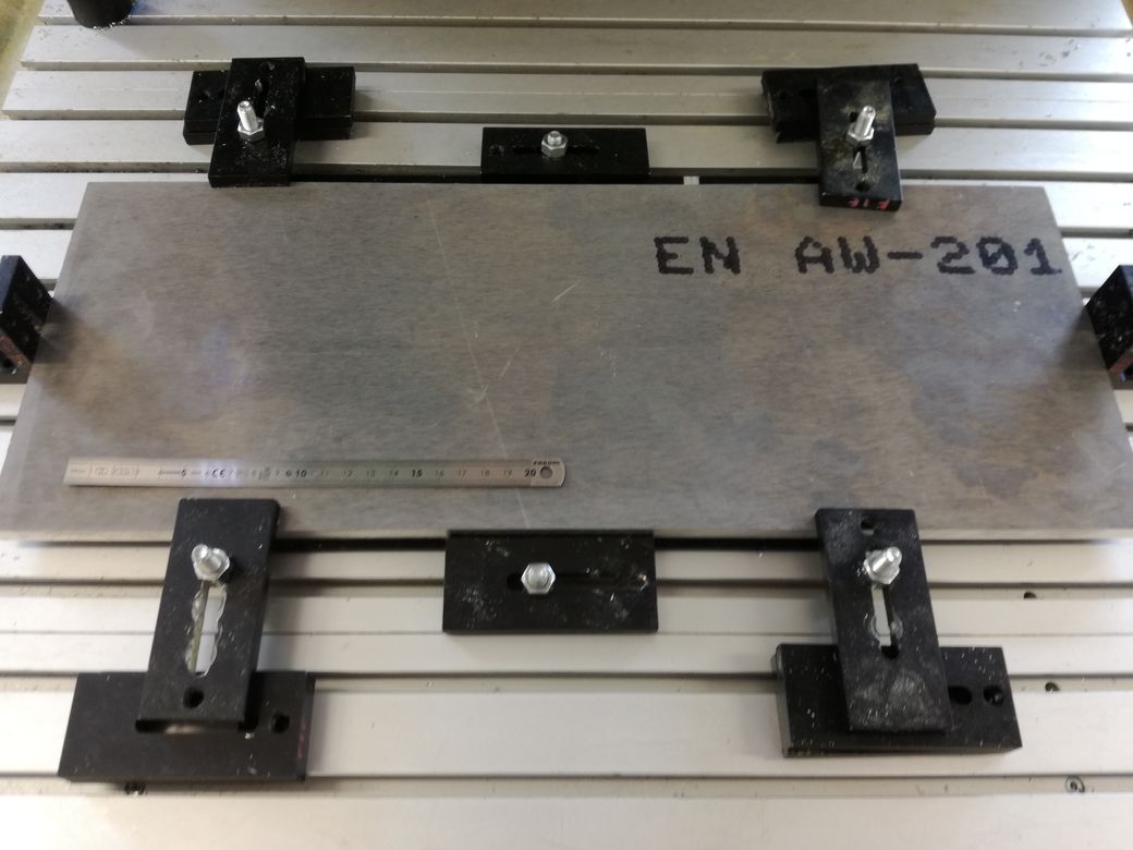
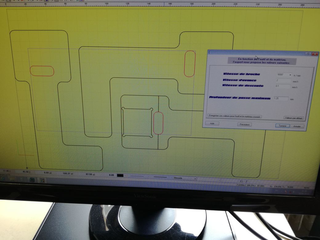
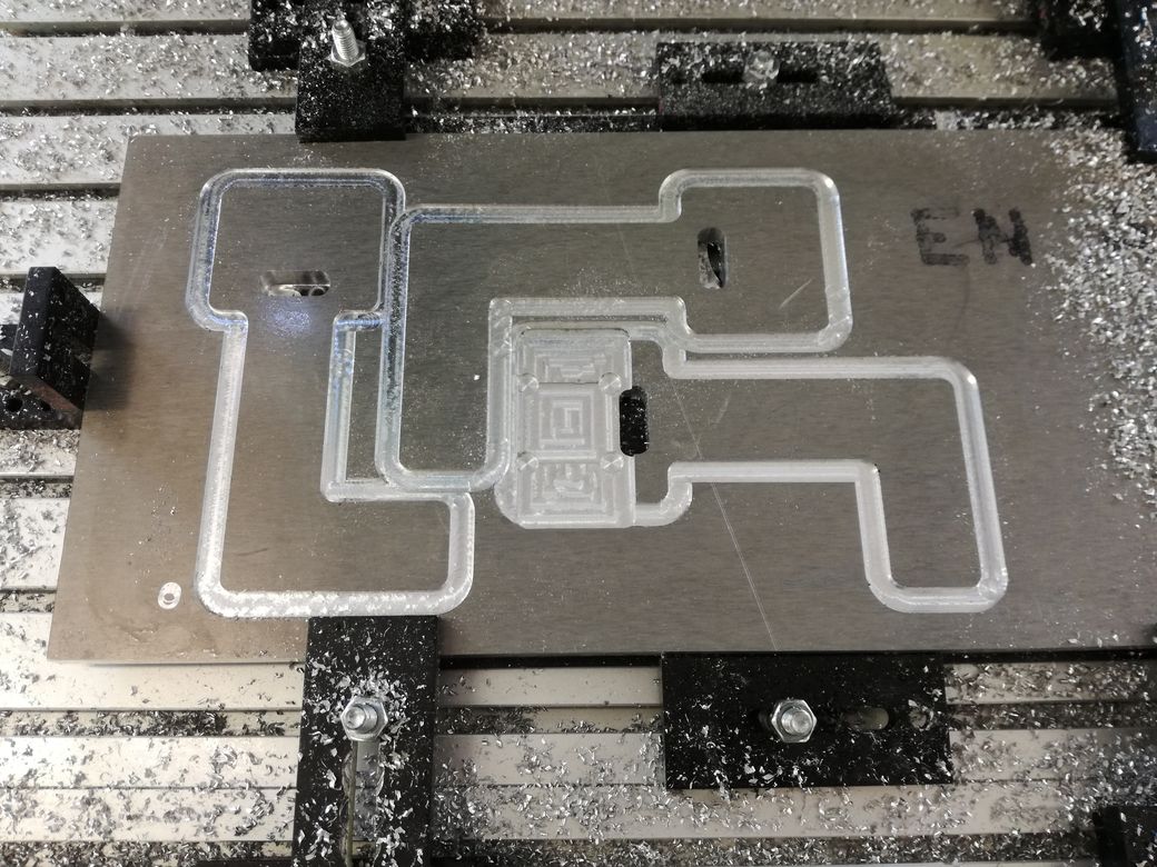
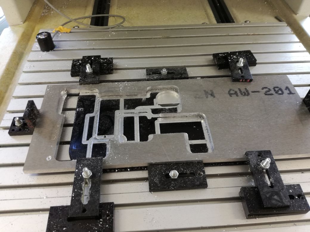
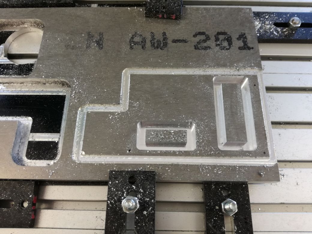
Machining
In my Computer controlled machining, I documented the milling of the Gamma Cool Box.
I hope it is big enough for the "make sth big" assignment.
Electronic design
Here is a hand sketch shematics of the PCB:
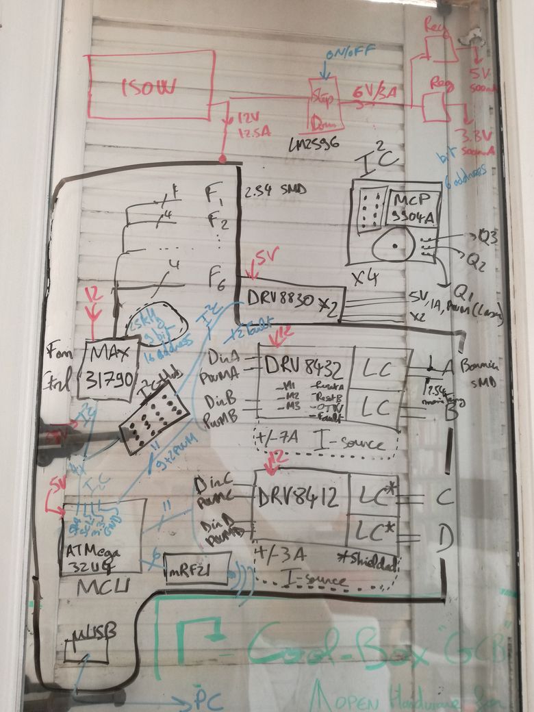
Track width for 35µm Cu PCB:
- 8A => 2mm (ΔT+50°C) - 1.5mm (ΔT+80°C)
- 5A => 1mm (ΔT+50°C) - 0.8mm (ΔT+80°C)
NB: Dissipation will be better if using
IMS PCB.
But through-hole componant would be very problematic...
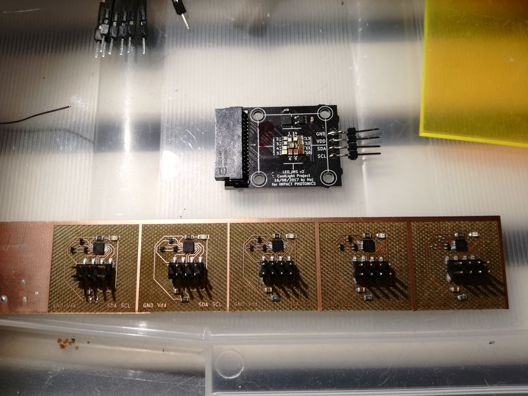
Designing the Probe PCB with KiCAD
1st part of my
Input devices assignment
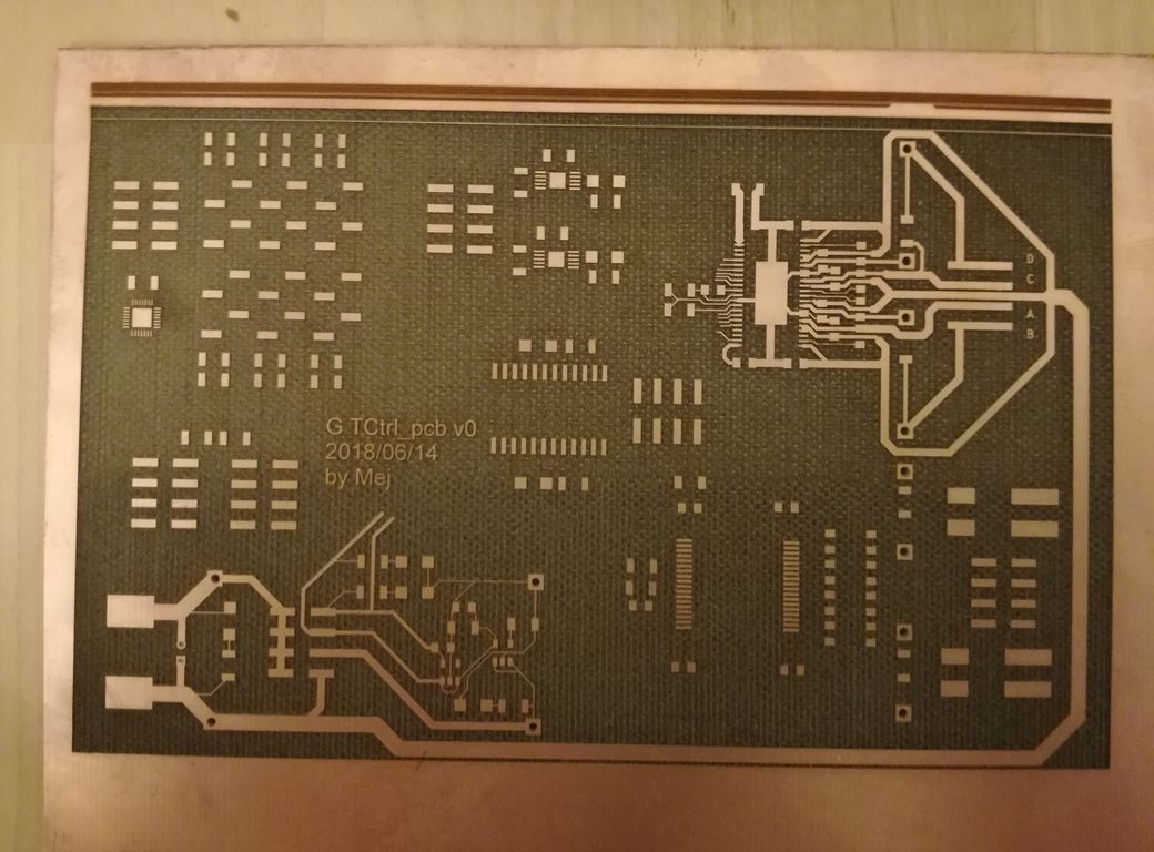
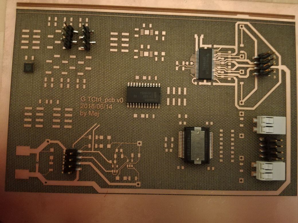
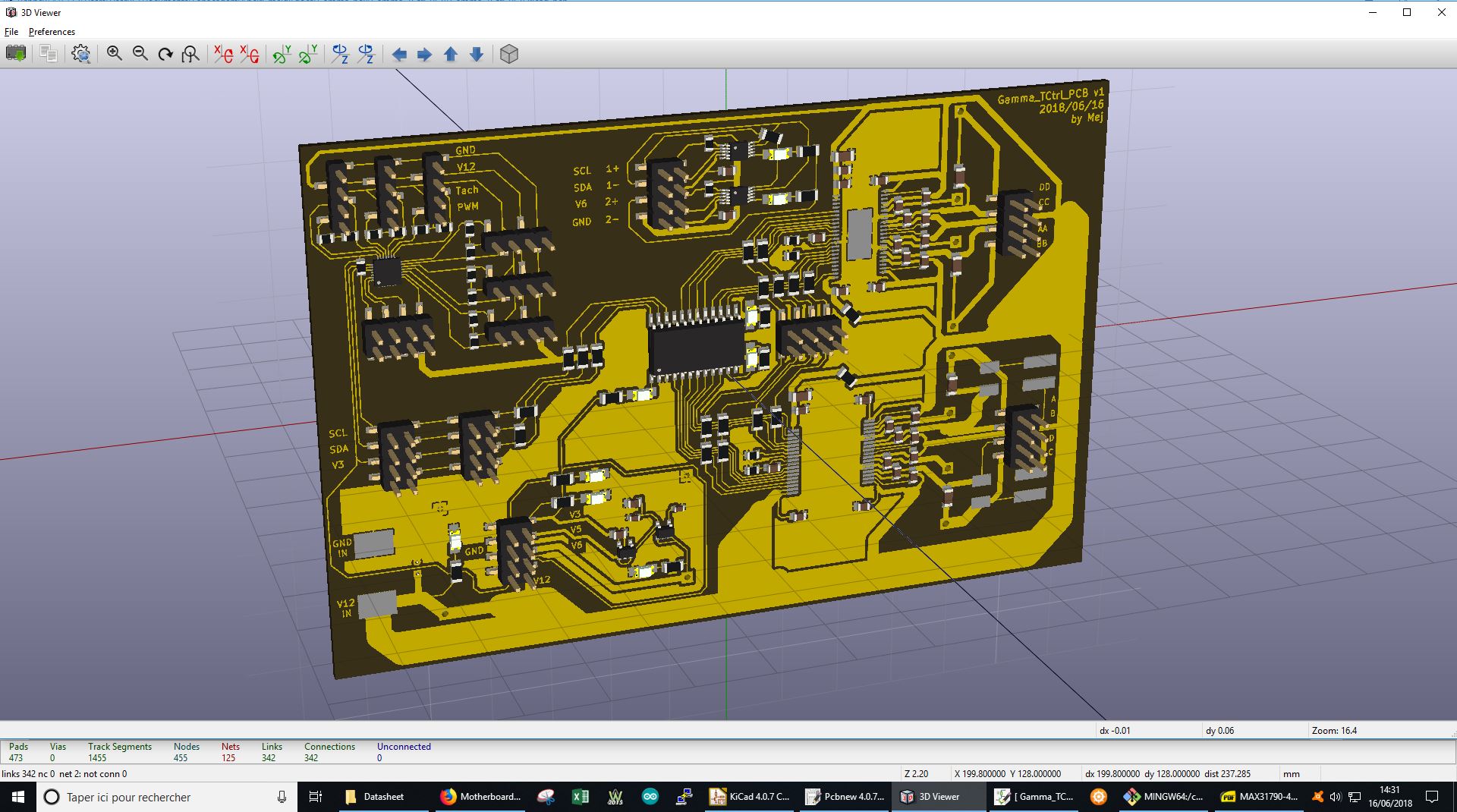
Designing the Main PCB with KiCAD:
1st part of my
Output devices assignment
Triage ALERTE
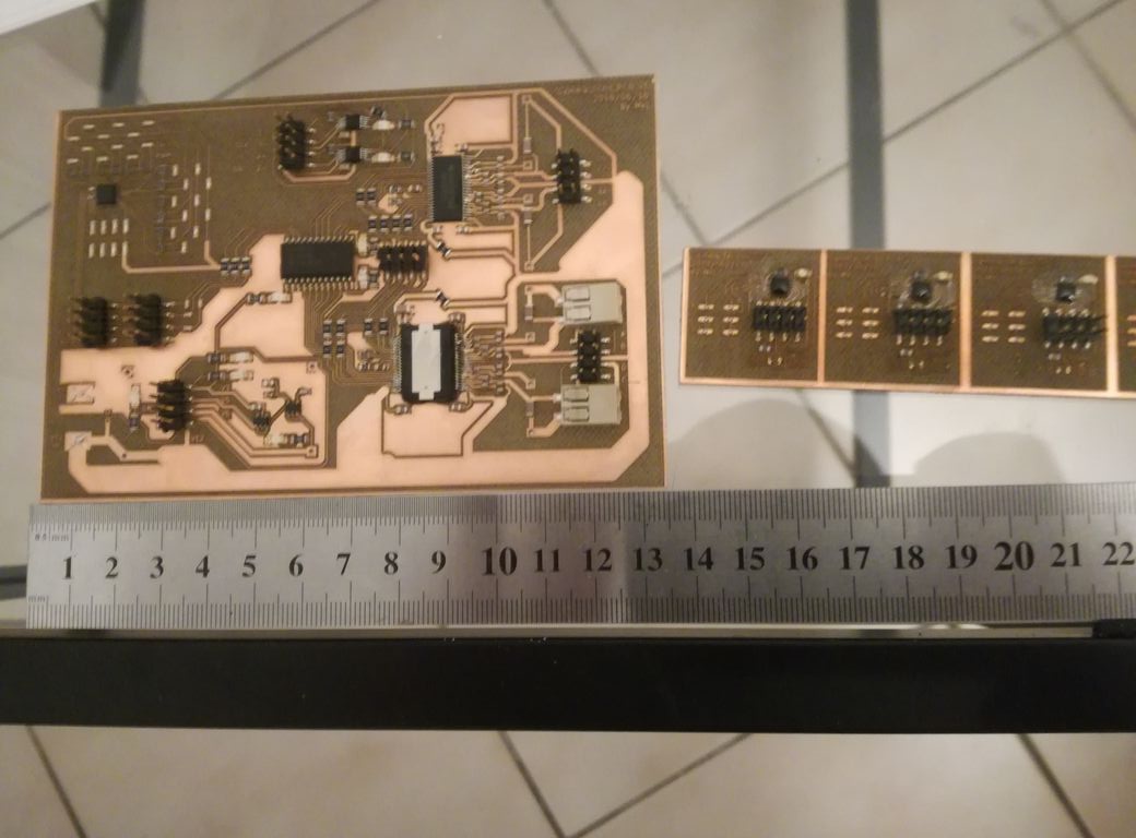
PCB production
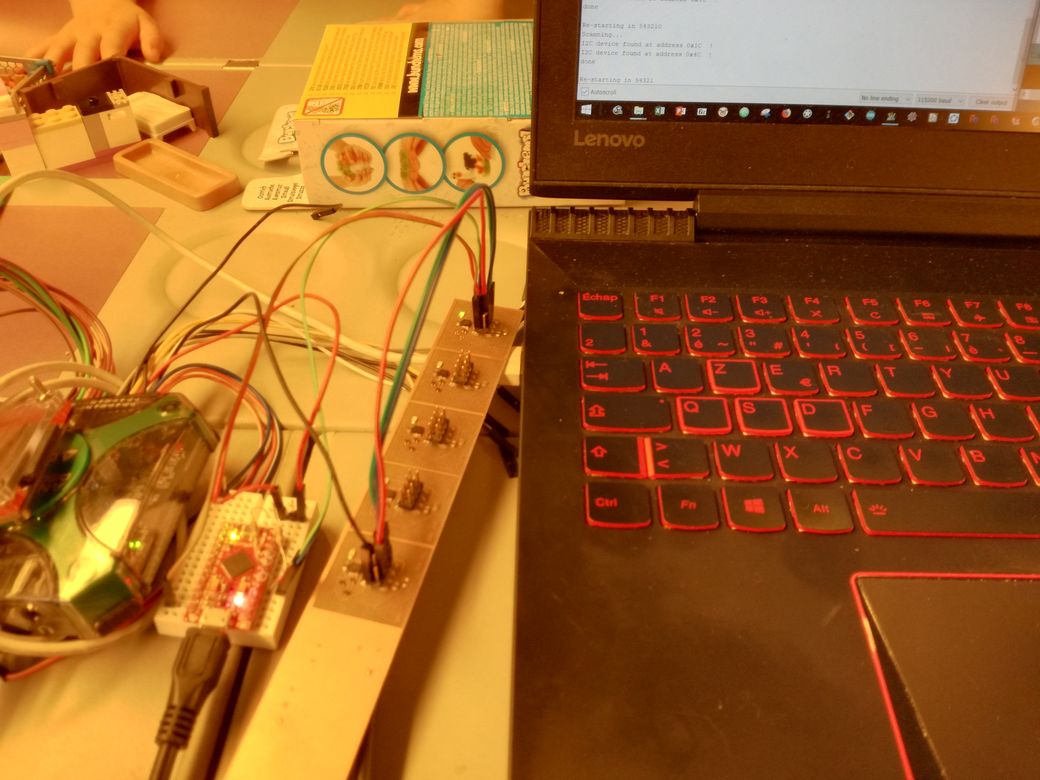
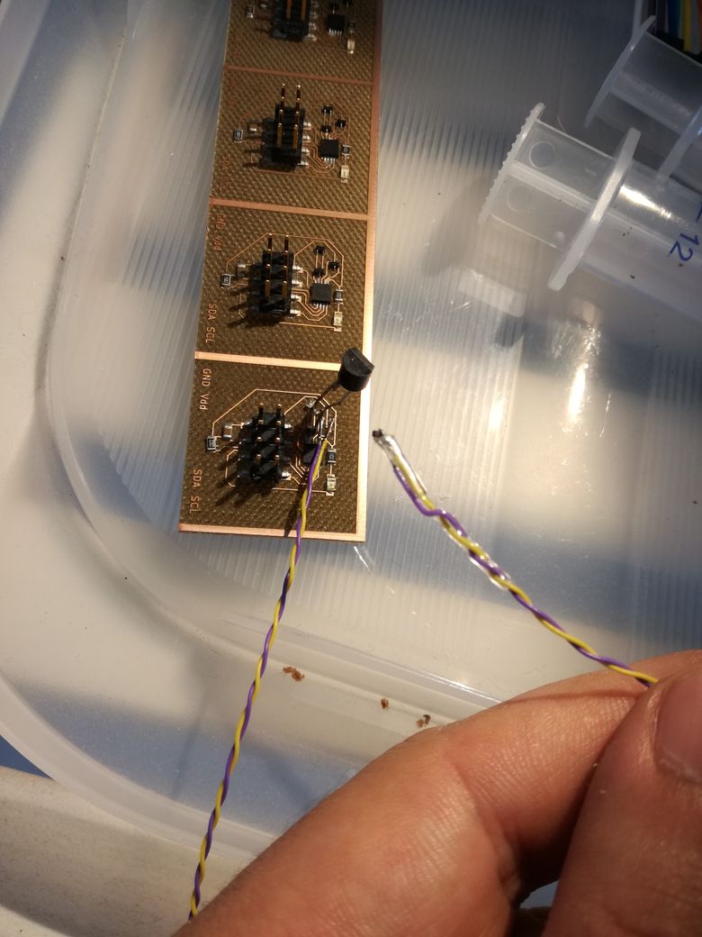
PCB Testing
Assembling
Back to Mejdi_FabAcademy_FollowUp
