Week 1 assignment
Principles and practices, project management (Jan 28)
Week 2 assignment
Computer-aided design (Feb 4)
Week 3 assignment
Computer-controlled cutting (Feb 11)
Week 4 assignment
Electronics production (Feb 18)
Week 5 assignment
3D scanning and printing (Feb 25)
Week 6 assignment
Electronics design (Mar 4)
Week 7 assignment
Embedded programming (Mar 11)
Week 8 assignment
Computer-controlled machining (Mar 18)
Week 9 assignment
Molding and casting (Mar 25)
Week 10 assignment
Input devices (Apr 8)
Week 11 assignment
Output devices (Apr 15)
Week 12 assignment
Composites (Apr 22)
Week 13 assignment
Networking and communications (Apr 29)
Week 14 assignment
Mechanical design, machine design (May 6)
Week 15 assignment
Interface and application programming (May 13)
Week 16 assignment
Applications and implications (May 20)
Week 17 assignment
Invention, intellectual property, and income (May 27)
Week 18 assignment
Project development (Jun 3)
Week 19 assignment
Project presentation (Jun 10)
Electronics design (Mar 4)
This week electronic again, but this time we have to design our first board. Designing electronic was something I always wanted to learn and this is the right opportunity. In this assignment we have to design and mill the hello board. This was quite easy thanks to my local instructor tutorial. The tricky thing was adding one LED and one button re-designing the traces without crossing them. In the end we have to solder all the components and to test the board uploading an example of code. Here below the summary and my experience with Eagle.
Summary:
Eagle
The tutorial was quite easy but without experience using Eagle I had some little problems. I started loading the libraries suggested:
1. Fab library
2. Sparkfun library
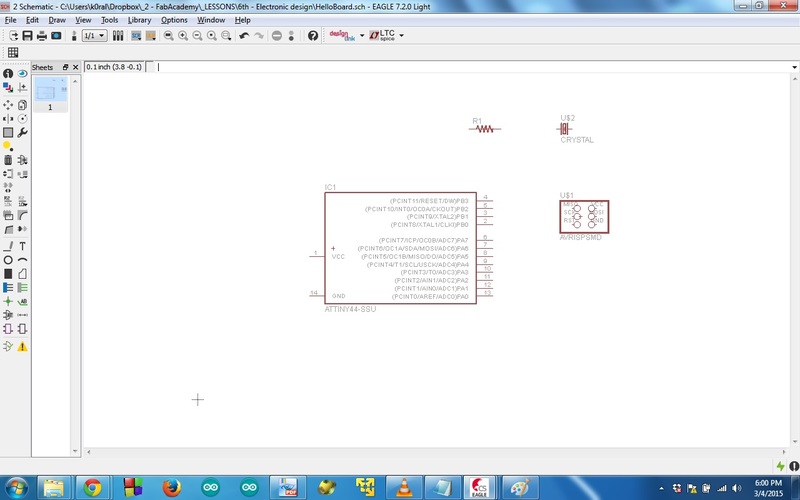
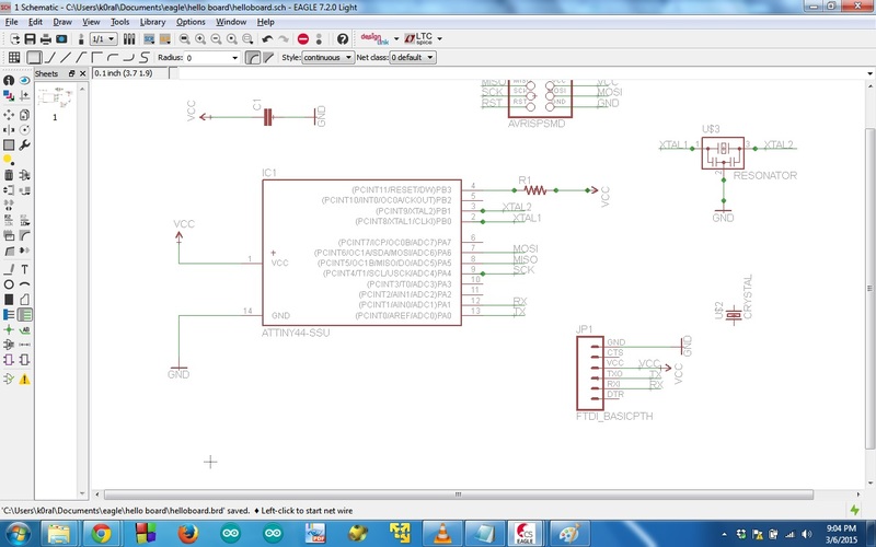
I started adding the first components: the Attiny44, the AVRISPSMD, one resistor and the crystal resonator. Here below you can see the schematic view of the circuit. You have to design your circuit using this view.
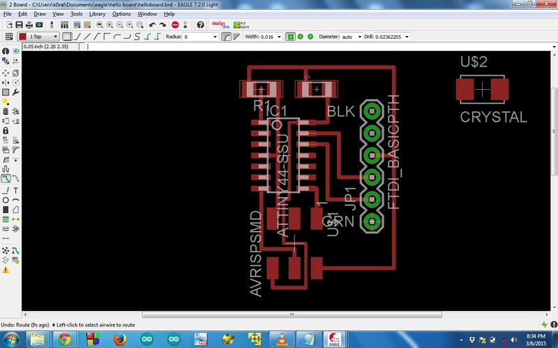
In correspondence to schematic view Eagle gives you the board view. This is where you have to work to decide how your circuit will be physically built by the milling machine.
I went on adding more components from the library and I started doing the first connections. There is a simple and clean way to wire the components, that is you have to use a line and to give it a label. Obviously if you give the same label in two points, Eagle understands (asking your confirmation) that you want to connect them.
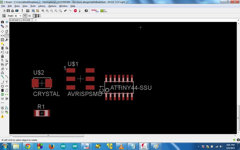
When you do the first connections you can see that in board view there are some yellow lines. These lines are the unrouted connections, that is Eagle tells you that you have to decide which will be the real trace and you have to design it. Below you can also see how are placed the Attiny44 and the AVRISPSMD. The first one is with the first pin (where you can see the white circle) on the top left corner. The second one (below the Attiny) has to be with the first pin on the top right corner. This is quite a standard disposal.
After a bit of designing I realized that the capacitor and the resonator was not the one I chose from the library. Choosing the right component it is not so easy. I tried to look at the drawing during the tutorial and I also looked at the package dimension. We used 1206 packages. You can find more details about SMD packages dimensions here.
The corresponding board view is this one below. I forgot to delete the wrong resonator (the crystal) in the schematic :)
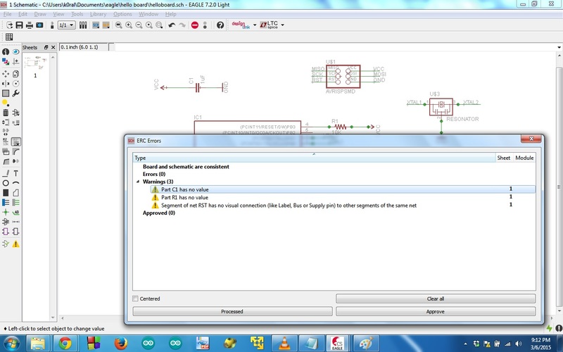
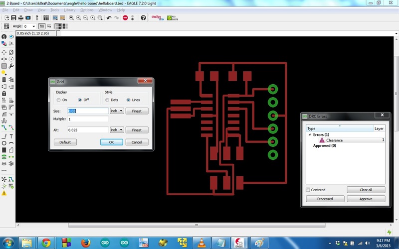
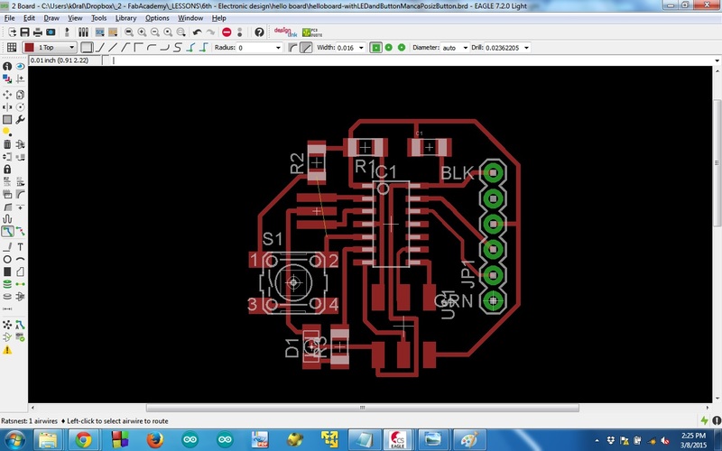
In the end of the design phase, Eagle helps you to correct some possible errors. Using ERC you can correct the errors in the schematic. You can see that Eagle suggested me that the capacitor and the resistor have no values. Moreover, I gave RST label but I forgot to show it (it was hidden).
Using the board view you can have the DRC which suggests you possibile errors you can do during the creation of the board. As you can see below Eagle suggested me that there was one trace that was too near one connection of the Attiny.
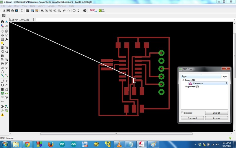
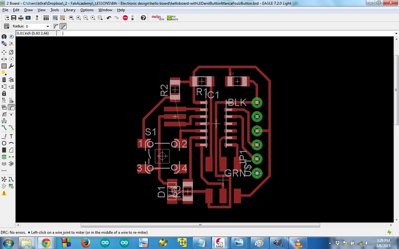
The solution was reducing the size of the trace from 0.016mm to 0.012mm and moreover you have to reduce also the size of the grid in Eagle.
After correcting the DRC error the board looks as below.
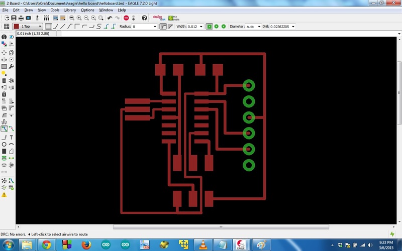
One good practice is to smooth the corners of the traces with the corresponding tool.
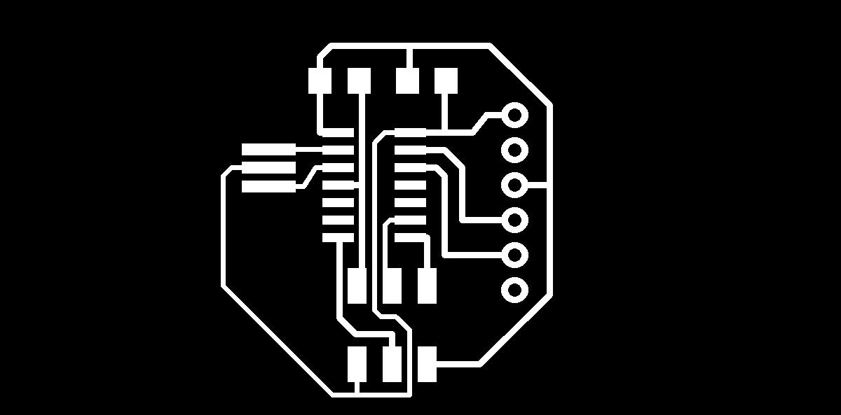
In the end you have to export the design to obtain a PNG image. You have do disable all the layers from the view menu, choosing layer settings and select only Top, via pads and pin layers. After that, you have to export with these settings:
- resolution: 500 dpi
- monochrome
- area: Full
This is the exported image
In order to make the soldering easier you can modify the image (I used Gimp) to have squared pads for the FTDI connector.
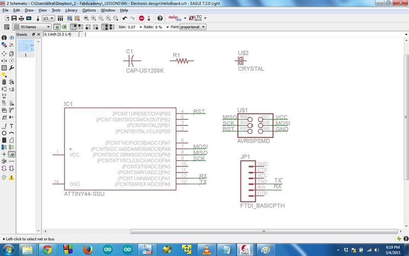
Now I had to add one button and one LED. First of all I had to understand which are the input/output pins of the Attiny. Reading the manual you can see that from PA0 to PA7 you have all the I/O pins. Pins are enumerated in the schematic view, but more important is to understand pins numeration in the board view because you have to place the components in such a way that it will be easy to design the connections avoiding to cross the other ones you have already done. The first pin was the one with the little dot (white circle in the board view) and in counterclockwise manner you will have the other pins.
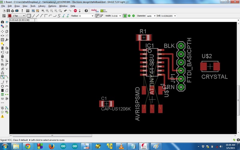
In the beginning I added the button in pin 10 but that pin was on the right of the Attiny and it was very difficult to find the right place location to connect the button without crossing the other lines I already did. I spent some time to think and it was a little bit frustrating, but in the end my local instructor helped me to solve my problem. It was quite easy but I still don’t have the right mental agility. More practice will help me :) Another trick is to let the lines go under some components. For example you can see the lines under the Attiny but you can also do lines passing under the resistor on under the button. Moreover, you have to know that the button has four pins but they are connected in pairs so it is enough if you connect two pins, that is 1 or 2 and 3 or 4.
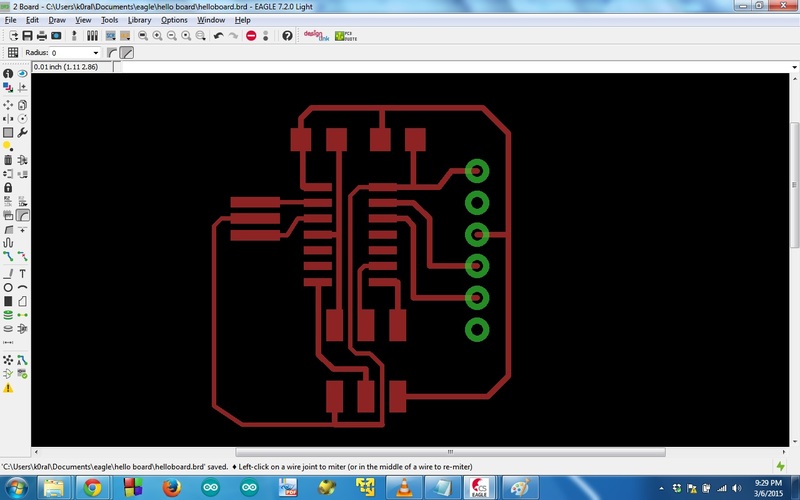
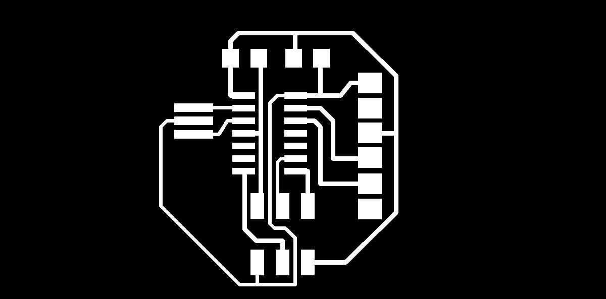
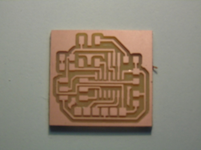
In the end I had this board below
This is the right one but I decided to reduce that space on the right side in order to have a more compact board
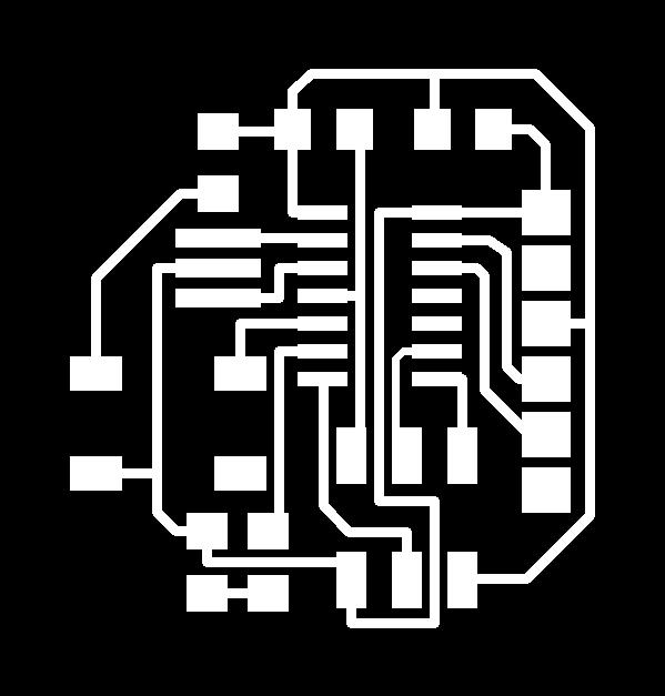
The final exported image to etch is this one
In order to drill the board I also did one image using the same size of the one exported but with white borders. Here below in the picture it is difficult to see it because of my white background color.

In the end I can show you my first designed board :)
Finally I soldered all the components and my local instructor helped me to verify the board uploading one code example.
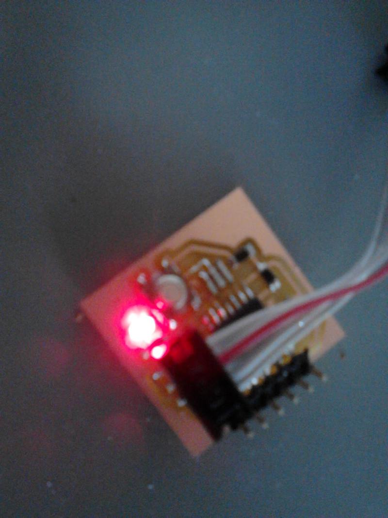
One error I did when I soldered the board was that I soldered the AVRISPSMD and the FTDI connectors with too short pins. I had to de-solder them with the hot air gun and I did two new connectors in such a way that I had the pins as long as possibile. I have to remember this lesson because if you have to de-solder the pins it is not so easy..
Conclusions
I was quite satisfied of this experience. I like electronic and I’d like to do more boards even for my pleasure. I hope I will find spare time in next days :)
Project files
Here are the files. You can find:
- png files to etch and to drill the board
- Eagle schematic and board file