8. Electronic Production
Toolpath Generation
The toolpath generation is a three-stage process: KiCad → Inkscape → MODS. Each stage has a specific job — exporting the design, preparing the image, and generating the machine instructions.
 - Electronic Production/Screenshot 2026-03-23 at 12.08.08 PM.png)
Stage 1 — Export from KiCad
In KiCad, go to File > Plot In the Include Layers tab, select the copper layer In the Plot on All Layers tab, select the edge cuts layer — this ensures both layers are perfectly aligned in a single file Make sure Negative Plot is checked — this inverts the image so copper appears black and the background white, which is what MODS expects
 - Electronic Production/Screenshot 2026-03-23 at 12.07.54 PM.png)
Export as SVG
Stage 2 — Prepare the Image in Inkscape
Open the SVG file in Inkscape Organize into three layers: Traces, Outline, Background Make sure the areas between paths are filled with white — this defines what the mill will remove Go to File > Export PNG Select Edit > Resize to Selection to crop the export to the exact scale of the drawing Set DPI to 1000 — higher resolution means more accurate toolpath generation Export two separate PNG files: one for the traces, one for the outline. Make sure both are the exact same dimensions.
 - Electronic Production/Screenshot 2026-03-23 at 12.06.59 PM.png)
Stage 3 — Generate Toolpath in MODS
Follow these steps in MODS:
- Open MODS and select: SRM-20 > Mill 2D PCB
- Load your PNG trace file
- Set the following parameters:
- Tool: 1/64 flat end mill
- Mode: Raster 2D
- Offset count: 4
- Speed: 2
- Origin: 0, 0, 0
Open the Edit Info panel to verify all settings Click Calculate — MODS will generate the toolpath and produce a G-code file ready for the machine
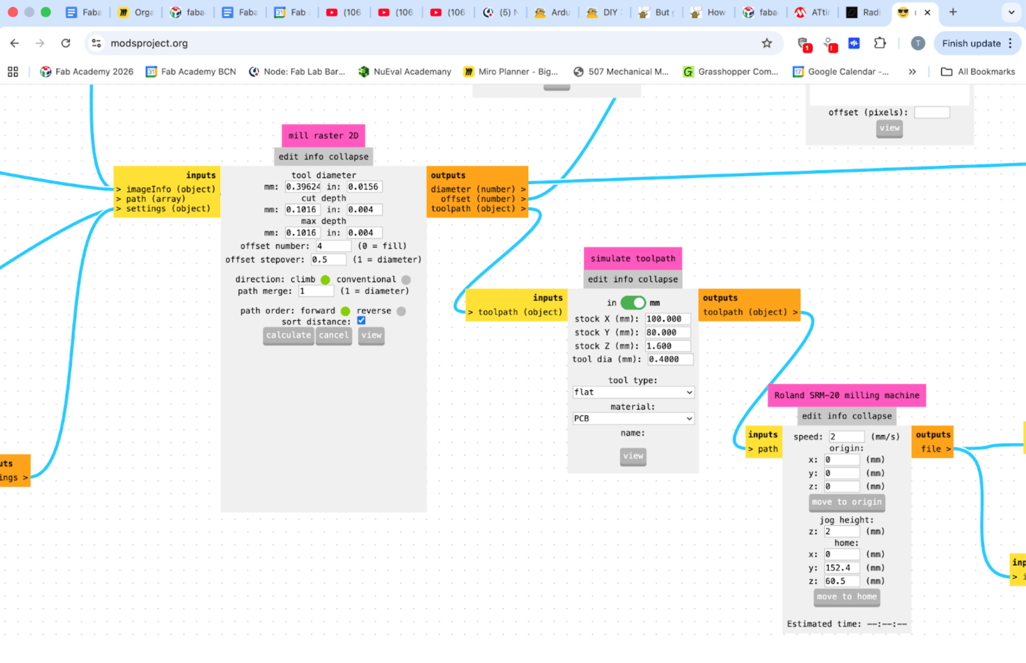
After all the settings are set we can calculate the toolpath and produce a G-code.
Milling — Roland SRM-20
- Fix the board — place the FR4 copper board firmly on the machine bed using double-sided tape. Press it down across the whole surface to avoid any flex or movement during cutting.
- Install the bit — insert the 1/64 flat end mill. This single bit handles both the trace engraving and the outer edge cut. Tighten it securely in the collet.
- Zero X and Y — using the machine’s control panel, jog the head and bed until the bit is positioned directly over the bottom-left corner of the board. Press Zero XY.
- Zero Z — move the bit to a central location on the board (centering reduces the risk of error across the surface). Lower the bit gently until it just rests on the copper surface. Re-secure the collet at this position. Press Zero Z.
- Run the job — send the G-code file to the machine. Watch the first few passes carefully — you want to see the copper being cleanly removed without cutting into the substrate beneath. Keep an eye out for dust buildup and clear it if it starts obscuring the cut.
 - Electronic Production/IMG_1987.jpg)
The board cut really well. Now its time to solder the components and make the circuit.
Soldering
Make Component List
Before soldering, compile a component list from your KiCad design and collect everything you need. Lay the components out so you can see them clearly and cross-reference against the board footprint.
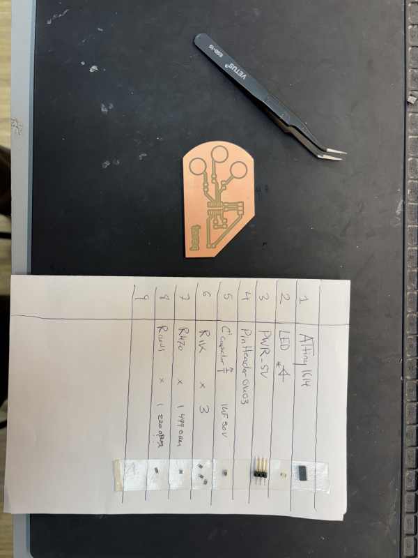
Now its time to solder.Solder in this order — smallest and most precise components first: * Tack each component in place — place a small drop of solder on one pad of each footprint. For the ATtiny, just one corner pad is enough at this stage. This is just to hold things in position.
-
Place and align — set the component onto its footprint in the correct orientation. Touch the soldering iron to the tacked pad so the solder melts, and use tweezers to press the component into position. Hold it steady as the solder cools.
-
Solder all remaining connections — once every component is locked in position, go back and solder all the remaining pads. Aim for joints that are smooth, shiny, and slightly domed. A dull or blobby joint usually means a cold connection — reheat it and try again.
-
Check clearances — look carefully for solder bridges between adjacent pads, especially on the ATtiny. Use a loupe or phone camera to inspect. A solder wick can remove excess if needed.
Here is the final result:
 - Electronic Production/IMG_2043.jpg)
Programming & Testing the Board
Setting Up Arduino IDE: * Open Arduino IDE and go to File > Preferences In the Additional Boards Manager URLs field, paste: http://drazzy.com/package_drazzy.com_index.json
-
Go to Tools > Board > Boards Manager, search for megaTinyCore and install it — this adds support for the ATtiny family of chips
-
Install the following libraries via Tools > Manage Libraries: Adafruit FreeTouch PTC (Peripheral Touch Controller)
-
Select your board: Tools > Board > megaTinyCore > ATtiny1614
-
Set programmer: Tools > Programmer > jtag2updi (or your UPDI programmer)
-
Connect your UPDI programmer to the 3-pin header on the board
Blink Debugging
Without a serial connection available, I used a technique called blink debugging to understand what the touch pads were reading. Rather than printing raw values to a monitor, I set different threshold values and observed how the LED responded — using the LED itself as a readout.
I changed the threshold in increments of 50 and recorded whether the LED turned on or off: Threshold LED 50 ON 100 ON 500 ON 1000 ON 1025 OFF 1050 OFF 1100 OFF 1250 OFF 1500 OFF
The board’s resting reading sits at around 1000. The LED turns on below this value and off above it — which told me that touching the pad was actually decreasing the reading rather than increasing it. I also noticed the LED dimming slightly near the threshold, which indicated the reading was hovering close to the boundary. This gave me a clear target for where to set the threshold in the final code.
Noise and Sensitivity
This process was a useful lesson in the real-world challenges of capacitive touch. The readings are sensitive to the electrical environment of the room — if the baseline drifts, false triggers can occur. At one point the entire board was responding to touch across all traces, likely because the traces were too close together and coupling capacitance between them. This is something to account for in future board layouts — wider spacing between touch traces reduces crosstalk.
The Code — Single Pad Test
const int LED_PIN = PIN_PA1;
const int TOUCH_PIN = PIN_PA4;
const int THRESHOLD = 100;
bool isTouched = false;

void setup() {
  pinMode(LED_PIN, OUTPUT);
}

void loop() {
  int reading = analogRead(TOUCH_PIN);

  if (reading < THRESHOLD) {
    isTouched = true;
  } else {
    isTouched = false;
  }

  if (isTouched) {
    digitalWrite(LED_PIN, HIGH);
    delay(200);
    digitalWrite(LED_PIN, LOW);
    delay(1800);
  } else {
    digitalWrite(LED_PIN, LOW);
  }
}
Group Project
This week the group characterized the PCB milling process on the Roland SRM-20, comparing three tools — a 1/64” flat end mill, a 15° V-bit, and a 30° V-bit. The main lesson was that small parameters like DPI, Z calibration, and cut depth have an outsized impact on trace quality — a single mismatch can throw off the entire result. In practice the 1/64” end mill proved more reliable and predictable than the V-bits, which are theoretically more precise but more sensitive to setup conditions.