Computer controlled cutting
Tasks
- Group assignment:
- ✔ Use the test equipment in your lab to observe the operation of a microcontroller circuit board
- Individual assignment:
- ✔ Use an EDA tool to design a development board that uses parts from the inventory to interact and communicate with an embedded microcontroller
- Extra credit: try another design workflow
- Extra credit: simulate your design
- ✔ Extra credit: design a case around your design
Group assignment
We did it all together in the FAB Lab Node Ilmenau. Bene was kind enough to summarize our labs group assignment.
Conclusion:
- Guidelines for using multimeters
- Stay within the same measuring range setting of the manual multimeter
- Always turn off/ disconnect power supply when changing the values to avoid voltage spikes.
- Always start measuring the higher values and then go smaller.
- The little hooks and crocodile tips rock!
- In the RIGOL there are two GNDs for measuring: 1 for bigger amperage and one for lower amperage. Same rules for the measuring ranges apply.
- Lab rules concerning small (or SMD) electronic components
- Only remove one container at a time and return it in the exact same spot you got it from to avoid confusion.
- Do not just remove the covering plastic foil but cut off whole package of SMD components always so it stays presentable.
- When assembling components for soldering, print out the BOM and paste electronic components behind each entry to avoid mix-ups.
- Only one person at a time removed SMD components from the containers to avoid confusion.
- Started by downloading and installing kicadFAB library
- Measured an Arduino Nano powered by computer USB port -> Results in table below.
- Measured Arduino Nano powered by a Laboratory DC Power Supply from GWINSTEK GPS-3303 and measured with a standard multimeter and the RIGOL DM3068. All went smoothly so we decided to measure for the minimum required Voltage. According to the datasheets, either 6 or 7V are the minimum Voltage. 12V is the maximum Voltage. We concluded that we agree with the datasheet.
| Power mode | 3.3V output pin | 5V output pin | Vin pin |
|---|---|---|---|
| Computer to USB | 3.291V | 4.71V | 4.31V |
| Input Voltage | Output voltage |
|---|---|
| 12V | 5.962V |
| 9V | 5.092V |
| 6V | 4.96V |
| 5.8V | 4.78V |
Measuring process: Connected one measuring probe to GND and the other to respective voltage pin. The measurements of the standard multimeter were pretty much the same as the ones from the RIGOL. Hence, in the table the more precise result will be displayed.
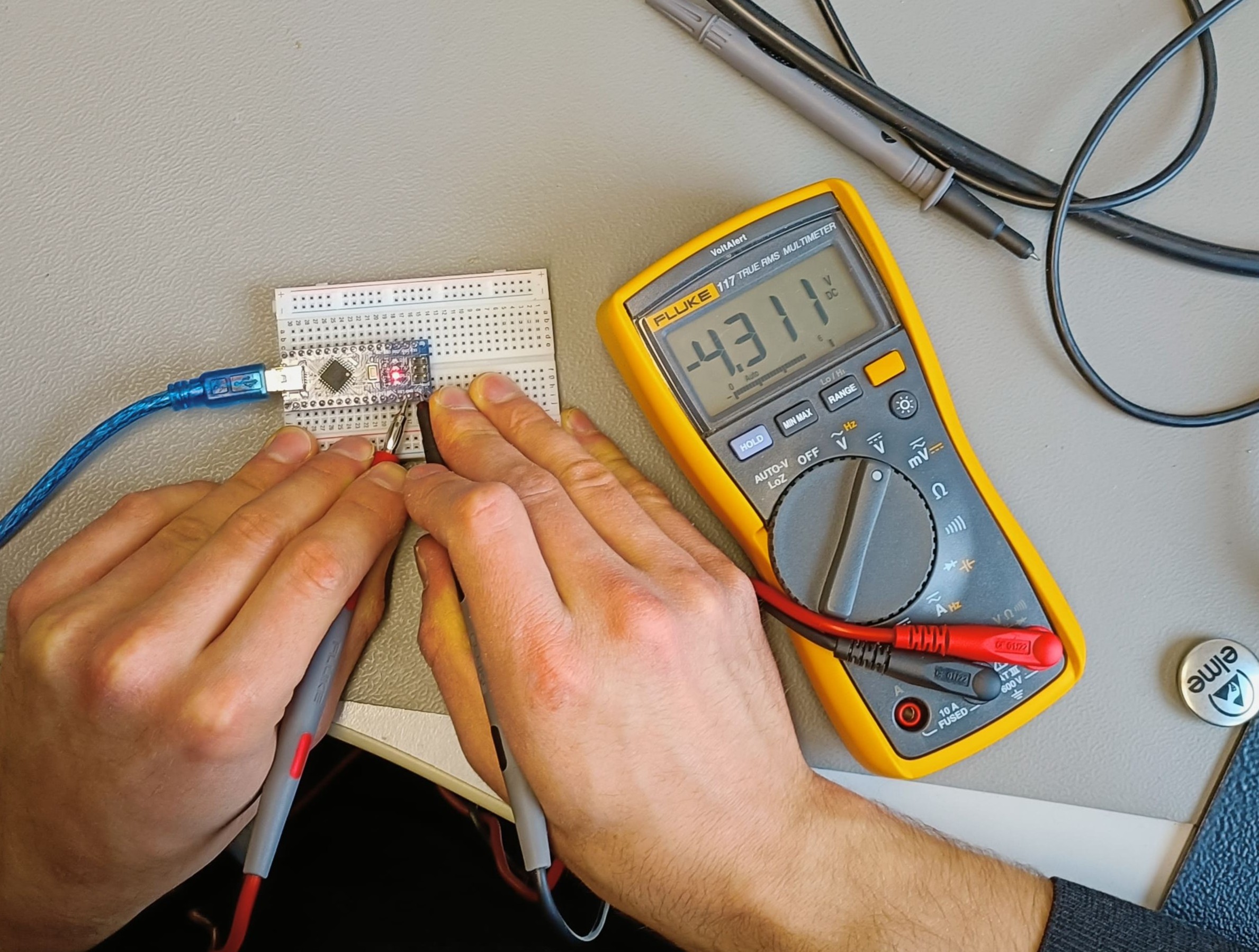
While measuring we discovered some weird phenomena. This list also includes random information our instructor gave us.
- Brown out: when the microcontroller notices the voltage is too low it raises a flag. Some microcontrollers automatically make a failsafe when this flag is raised. Some microcontrollers can also be programmed to do sth else when this happens.
- Vin for some reason already has a voltage applied to it when we were powering the Nano from the computer. We did not figure out why.
- When designing PCBs: widen the pads and traces required for higher amperage and connect the components in parallel. The traces can become smaller the more parallel branches have already been fed.
- When designing PCBs: fragile signal connections always in series.
Test PCB board
Functions: blink an LED either on it's own (when button is pressed) or via the XIAO.# This is the Link to the website I found the original schematic from. I did change it a little bit to add a button and the Xiao. I had some old 555 timer chips laying around and wanted to use them.
Download files:
- Download: Panel testingProduction KICAD_PCB
- Download: TestingProduction KICAD-SCH
- Download: TestingProduction 7Z zip file
I found this tutorial incredibly good. I recommend watching it.
Process of preparation to create your own PCB:
- Make schematic like usual.
- Once done, make sure the footprint are available. It is possible to create your own but quite annoying.
- Close the schematic editor and open the PCB editor by clicking on the green icon.
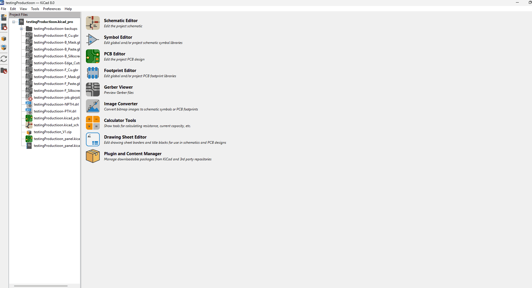
Menu selection Kicad from main page - Click "tools-Update PCB from Schematic" and place components.
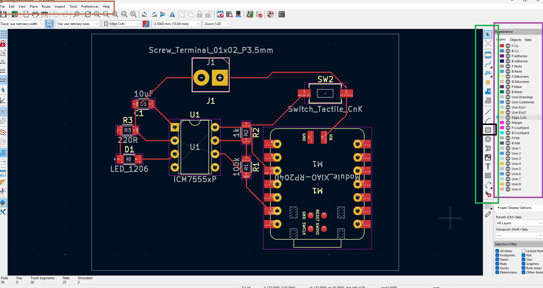
Layout PCB Editor Kicad - Select the "Edge.Cuts" in the appearance (purple menu).
- Draw a rectangle (black symbol) from the draw tool bar (green menu) and dimension it accordingly by double clicking on it.
- Organize the "ratsnest" (initial automatic placements of all components) in a way that the least possible amount of traces/ wires/ connections cross paths. The thin lines indicate which components belong together. There are tools for this, but manually is faster. Press "r"
- Start drawing traces by clicking on the blue symbol in the green menu until everything is connected.
- Optional: click on View-3D viewer (brown menu) to see how it will look like when produced.
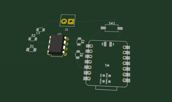
3D view of PCB board - Export to gerber
- Select File (in brown menu) - Fabrication Outputs - Gerbers - Plot
- Generate Drill Files - Generate Drill File - Close
- Close PCB editor back to main page
- View - Browse Project Files; Zip into Archive all .gbr & .drl files you find
- Check gerber file: initial page - gerber viewer - File - Open ZIP File archive
Electric schematic puzzRob
Go to the final project page for more information and context.
More information on choosing components: BOM choosing components
Download files:
- Download: all schematics V1 PDF
- Download: kicad file RFIDModule V1 KICAD_SCH
- Download: kicad file battery and charging circuit V1 KICAD_SCH
- Download: kicad file linear buck converter V1 KICAD_SCH
- Download: kicad file switch boost converter V1 KICAD_SCH
- Download: kicad file user interaction V1 KICAD_SCH
- Download: kicad file block diagram-ish circuit V1 KICAD_SCH
- Download: kicad project file V1 PRO
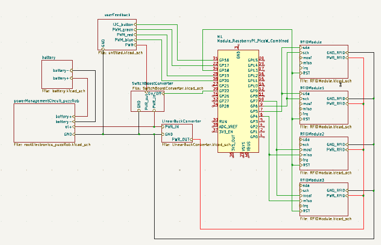
Process of designing schematic
- Prepped Kicad. Installed FAB library following this tutorial. (This is a bit tricky because knowing the exact location files on computer is necessary)
- Learned how to manage multiple sheets in Kicad for modular designing.
- Designing User Interaction module. Considered options:
- Charlieplexing: use basic electronic rules to control multiple LEDs in a matrix with a minimal amount of pins. Video Explanation This can also be done with buttons or RGB LEDs
- Common Cathode configuration: using transistors to control multiple RGB LEDs. Alternative: Common Anode Configuration. For this project I choose the common cathode configuration because I employed a ground-logic approach.
- Neopixels: standard and easy solution for this kind of problem. Relatively expensive though.
Main problem remains: 3A required to power 5 RGB LEDs. See Comparisons of solutions for more information why I eventually chose to go only with an RGB Arcade Button.
Power consumption of other components:
- Power Management circuit and charging circuit:
- General information on power management
- The RFID modules require a constant 3.3V power supply with little to no noise. Input from a 1s battery=3.7V -> Linear Buck Converter
- Charging circuit. 2 ICs were recommended online:
- MCP73831/2: I did not find much more on it and no recommended IC protection circuit.
- TP4056: . It is used for LiCoO2 and LiMn batteries. Complete module for buying
- Looked for possible batteries: SONY MNCOO2 3.7V 3120mAh
- Due to the high cost and high power consumption of the LEDs, I decided to look for alternatives. I found the IC MC34063AP Information about this decision process
- Research on specific requirements in PCB production.
Apart from the standard PCB milling production they can also be
created with a Vinylcutter. Two approaches:
- Use a conductive (copper) base and stick the not conductive layers on top. Not preferred due to environmental and socioeconomic impact.
- Use a non conductive base and stick the conductive traces onn top. Example: Aluminia base and copper traces cut from copper foil. Example 2: PCBs on glass with copper traces. Src 1 Src 2
- Defining Pinout of Pico:
Additional footprints:
Datasheets:
Comparison: Kilobot
Current market leader due to small size and wide range of applications as well as ample development from Harvard University. Creators: Michael Rubenstein and Prof. Radhika Nagpal. Cost: 14€ per robot, Size: height= ~3cm; Diameter 3.3cm
Issue card
What I struggled with this week:
- Kicad neither had the components or the footprints. Solution: googled them and found them on Snapeda website for free. I also considered doing them myself but problem #2 deleted the initial design that I had made and I got fed up with it.
- Other sheets and sub sheets in kicad: when creating a new sheet (Ctrl+s) it will make you create 2 sheets. Haven't quite figured out what the second one is for yet. However, if the name is not changed and you use that page, it will overwrite whatever you did on a different sub sub page (Hence how I lost my custom design of the footprint component). Solution: Name that second sheet exactly like your first one. This will prevent the overwriting and if the second page ever comes to play, you will always know to what sub sketch it belongs.
What I learned in electronics design:
- I understood how a datasheet is employed effectively thus not making me dependent on online tutorials to design circuit from here on.
- Understood how to calculate values for components. Though they taught us in uni classes, it was a hole different thing applied to my ambitious final project.
- Been reading about more efficient study modes.
- Been studying Dutch for some reason.