Week 8 Group Assignment: PCB Design Rules Characterization and Manufacturing
Introduction to the Lab's Small CNC Machine
At Chaihuo Makerspace, we use a small CNC engraving machine JY5300-2 manufactured by Jingyan Instruments, which can be controlled via computer and wired remote control. Matthew provided training and guidance on using the equipment.
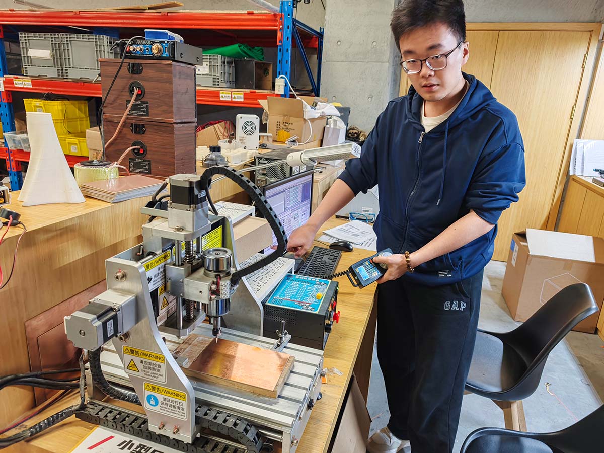
The small CNC engraving machine at Chaihuo Makerspace, with Matthew training us on how to use the equipment
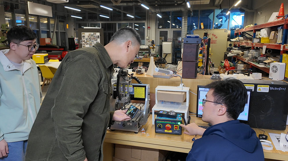
The button Matthew is pointing to, which is the PC connect/disconnect button on the control box
The main technical specifications of the machine are as follows:
- Work table area: approximately 40cm x 30cm
- Maximum engraving depth: approximately 5mm
- Positioning accuracy: 0.01mm
- Repeatability: 0.05mm
- Control method: Parallel port connection to computer
- CNC control software: Mach 3
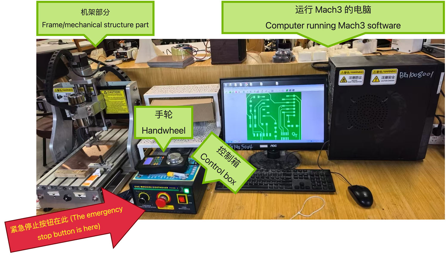
The small CNC engraving machine produced by Jingyan Instruments
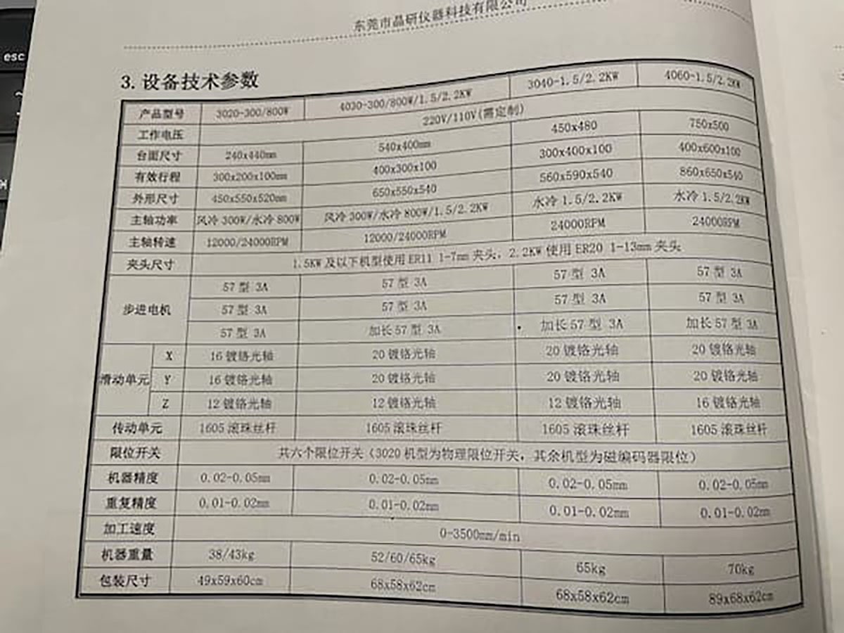
Parameter table from the equipment manual
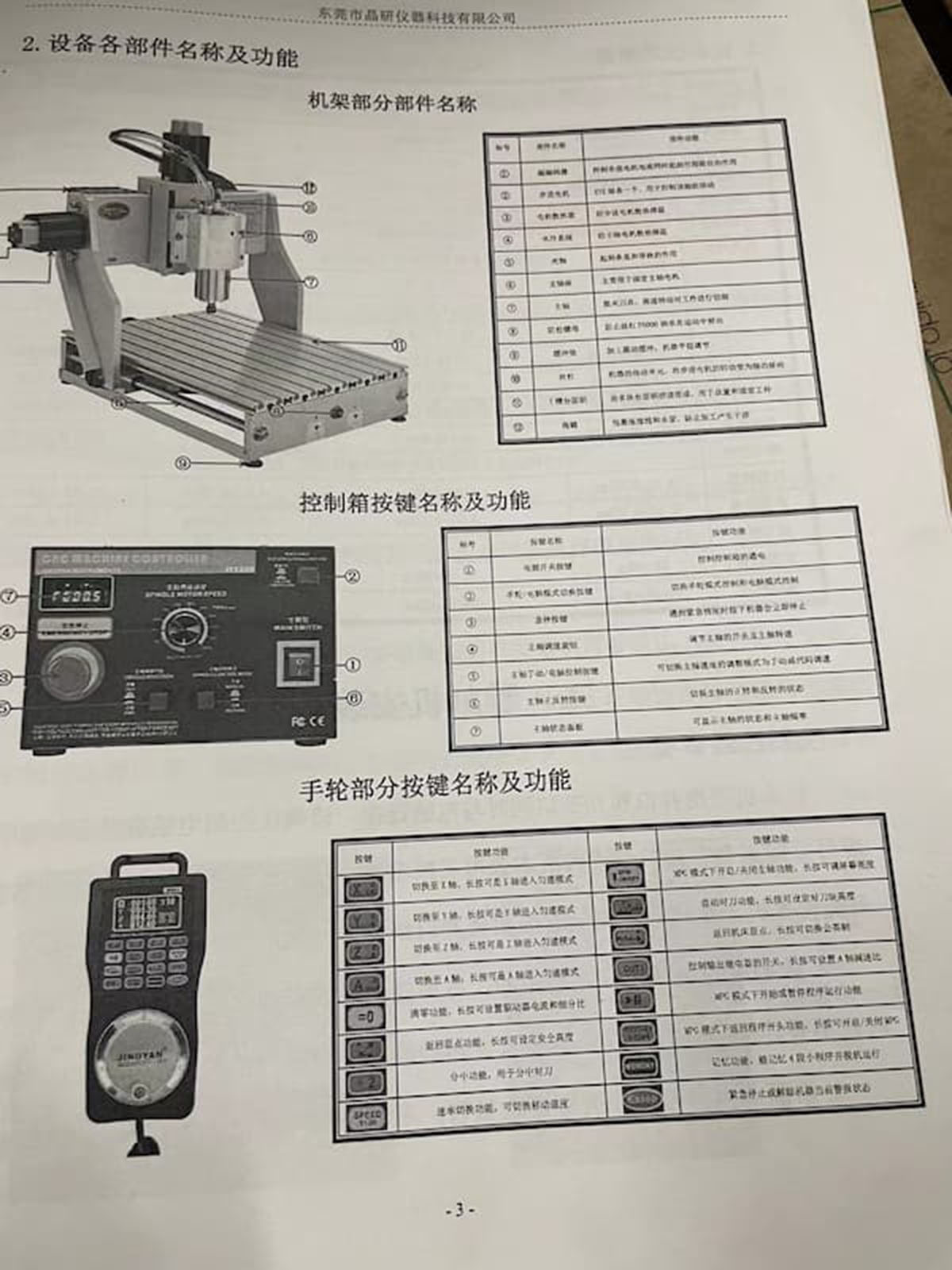
Function key description from the equipment manual
Tools and Materials
Cutting Tools
The lab is equipped with various milling bits to meet different cutting needs:
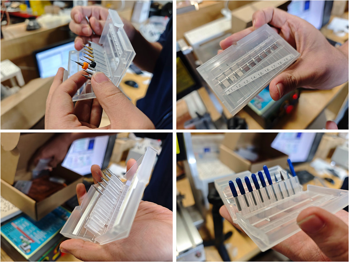
Various types of cutting tools: 1/64 inch end mill, 1/32 inch end mill, and V-shaped bits
We primarily used the following tools for this assignment:
- 1/64 inch (0.4mm) V-shaped bit (left in image below): Used for fine cutting of circuit traces
- 1/32 inch (0.8mm) straight slot end mill (right in image below): Used for drilling holes and cutting circuit board outlines
After comparative testing, the V-shaped bit produced better results when cutting circuit traces, with a smoother and flatter surface.
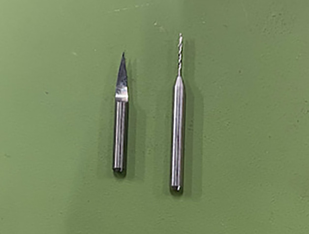
The 1/64 inch (0.4mm) V-shaped bit (left) and 1/32 inch (0.8mm) straight slot end mill (right) we prepared to use
PCB Materials
We used standard single-sided copper-clad boards:
- Material: FR-1/FR-4 fiberglass epoxy board
- Thickness: 1.6mm
- Copper layer thickness: 35μm (1oz)
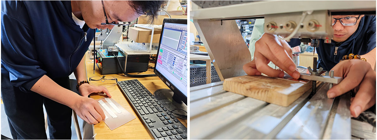
Before cutting the copper-clad board, double-sided tape needs to be applied to the back to fix it more securely on the wooden board serving as a base. The copper-clad board attached to the wooden base must then be secured with fixtures
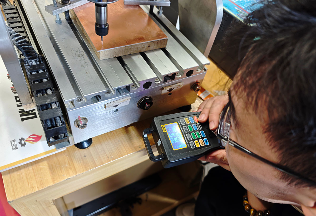
Matthew instructing us on how to zero the equipment and calibrate the Z-axis height
Workflow and G-code Generation
The CNC machine requires G-code to execute cutting operations. We used Mods CE to convert images:
- Visit the Mods project website
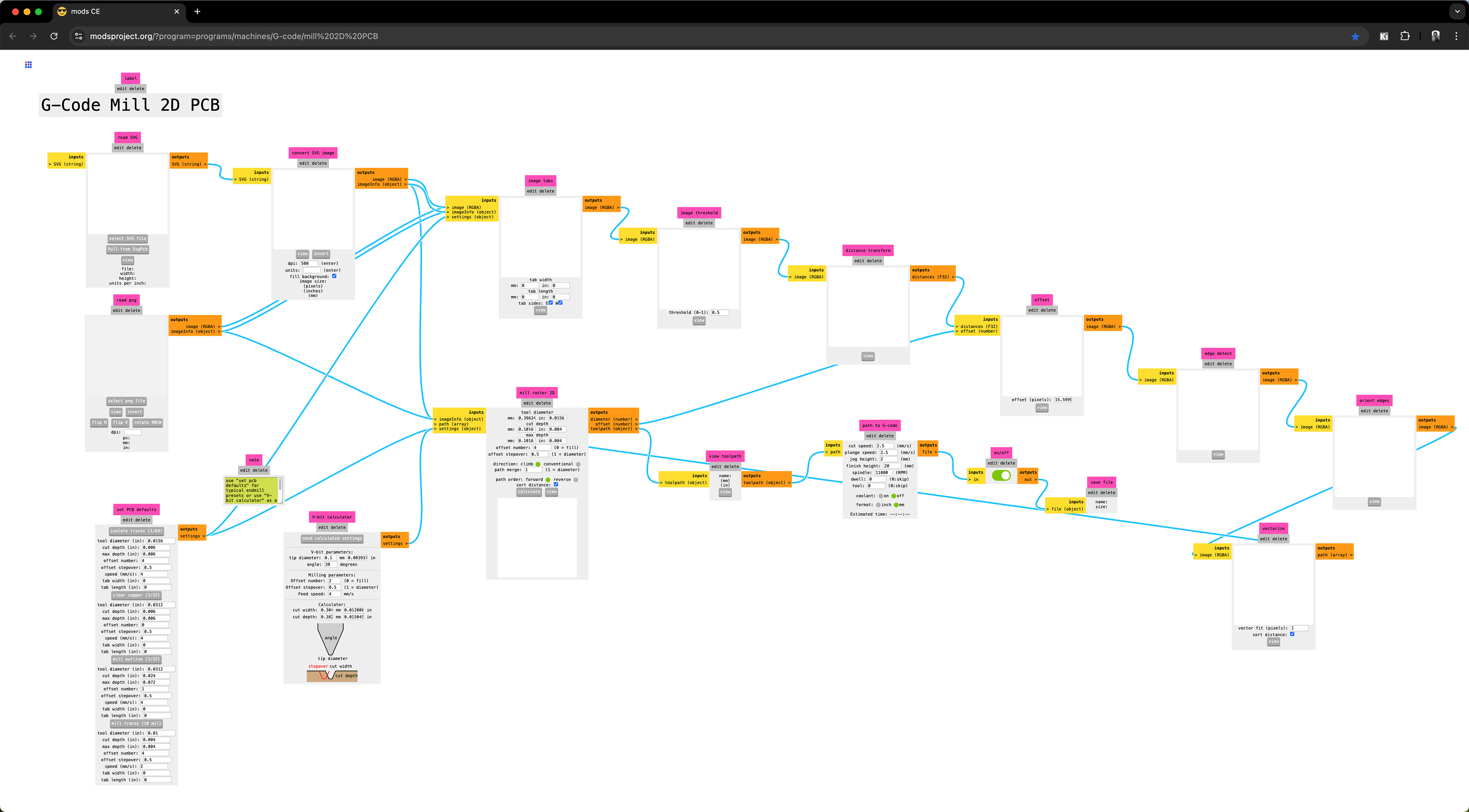
G-Code Mill 2D PCB
- Upload image files in PNG or SVG format (lossless resolution format)
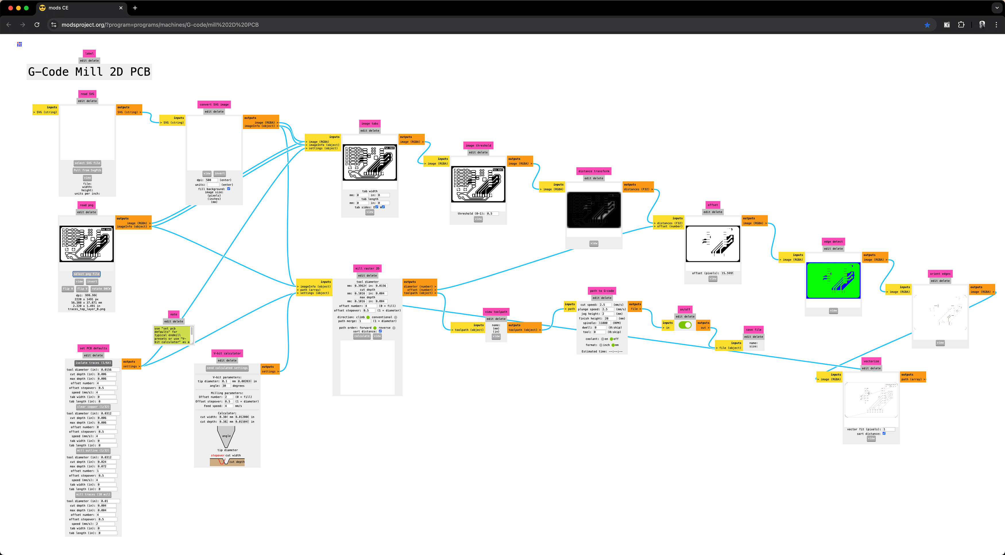
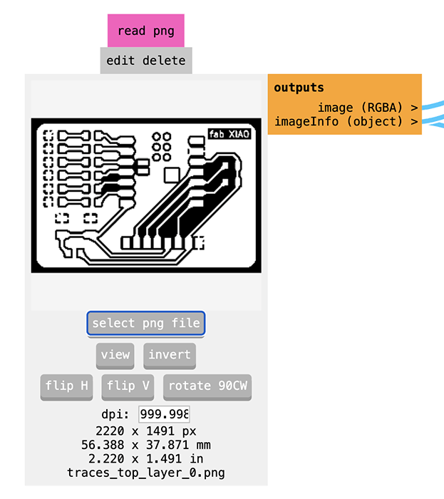
This interface is the module in MODs software for importing and processing PCB design PNG files. Here's an explanation of the various elements' functions:
Top Control Area
- read png: The name of the current module, used for reading and processing PNG image files.
- edit delete: Options to edit or delete the current module.
Central Area (Image Display)
- Displays the currently loaded PCB design image (here it's the PCB trace layout for the XIAO extension board).
- The image is displayed in black and white, where black areas represent copper layers and white areas represent areas to be milled.
Bottom Control Buttons
- select png file: Click to select and upload a PNG file
- view: View the full view of the current image
- invert: Invert the image colors (black becomes white, white becomes black), used to convert milling strategy
- flip H: Horizontally flip the image
- flip V: Vertically flip the image
- rotate 90CW: Rotate the image 90 degrees clockwise
Image Information Area
- dpi: Image resolution (dots per inch), set to 999.998 here
- 2220 x 1491 px: Image pixel dimensions (width x height)
- 56.388 x 37.871 mm: Actual physical dimensions (in millimeters)
- 2.220 x 1.491 in: Actual physical dimensions (in inches)
- traces_top_layer_0.png: Name of the currently loaded file
Right Output Area
- outputs: Output information area title
- image (RGBA): Output image data (RGBA format)
- imageInfo (object): Object containing detailed information about the image
Important Usage Notes
- Importance of DPI setting:
- The DPI value determines the conversion ratio from pixels to actual physical dimensions
- Ensure the DPI setting is correct, otherwise the milling dimensions will be inaccurate
- Image orientation:
- Use the flip and rotate buttons to ensure the image orientation is correct
- Need to adjust according to your CNC machine coordinate system
- Invert function:
- Black areas represent the parts to be milled away (i.e., circuit isolation grooves)
- White areas represent the copper layer to be preserved (i.e., circuit traces and pads)
- In the PCB milling process, the CNC machine will mill along the black lines and areas, removing the copper layer to form isolation grooves, thereby creating the desired circuit pattern. If the imported image is contrary to this convention (e.g., white represents the part to be milled), the "invert" button needs to be used to invert the colors.
- Dimension confirmation:
- Before actual milling, confirm that the displayed physical dimensions (mm or in) match your expected design dimensions
After importing the PNG file, you need to pass this image to the milling modules we discussed earlier (such as isolate traces, mill outline, etc.) to generate the actual G-code file for the CNC machine.
- Configure cutting parameters
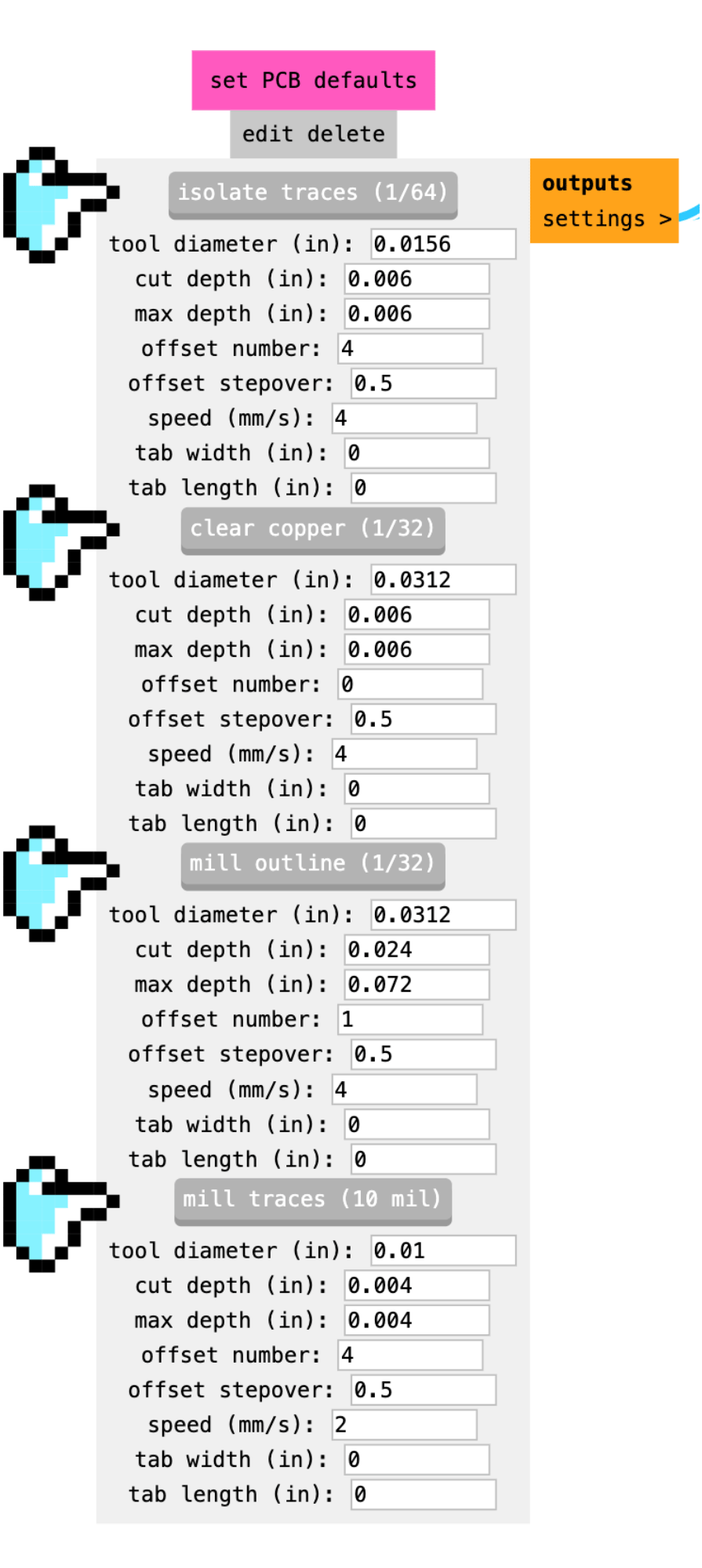
This image shows the default parameter settings for PCB milling in the MODs software. Here's a detailed explanation of the parameters:
Overall Function Area
- set PCB defaults: Set default parameters for PCB milling
- edit delete: Edit or delete current settings
Process Types (Four Different Processing Methods)
- isolate traces (1/64): Isolate traces (using 1/64 inch tool)
- clear copper (1/32): Clear copper layer (using 1/32 inch tool)
- mill outline (1/32): Mill board outline (using 1/32 inch tool)
- mill traces (10 mil): Mill fine traces (using 10 mil tool)
Common Parameters Explanation
Each process has the following parameter settings:
- tool diameter (in): Tool diameter (inches)
- Different processes use different size tools (ranging from 0.01 inch to 0.0312 inch)
- cut depth (in): Single-pass cutting depth (inches)
- Represents the depth cut in each pass
- Trace isolation typically at 0.004-0.006 inches
- Outline cutting is deeper, at 0.024 inches
- max depth (in): Maximum cutting depth (inches)
- Total depth of milling
- For outlines, set to 0.072 inches (about 1.83mm), slightly greater than standard 1.6mm PCB thickness
- offset number: Number of offsets
- Represents the number of cutting passes around the target path
- Trace isolation typically set to 4, ensuring complete isolation of copper lines
- Outline cutting only needs 1 precise cut along the line
- offset stepover: Offset step amount
- Overlap ratio between adjacent cutting paths (0.5 represents 50% overlap)
- All processes set to 0.5, which is a value balancing efficiency and quality
- speed (mm/s): Cutting speed (millimeters per second)
- Speed at which the tool moves
- Coarser tools have faster speeds (4mm/s)
- Fine tools reduced to 2mm/s to avoid damage
- tab width (in) and tab length (in): Width and length of connecting tabs (inches)
- Small connection points preserved when cutting outlines, preventing the board from detaching before cutting is complete
- Set to 0 indicates no tabs are used
Process Characteristics Comparison
- Isolate traces (1/64):
- Uses fine tool (0.0156 inch/about 0.4mm)
- Shallow cutting (0.006 inch)
- Multiple offsets (4 times) ensure traces are completely isolated
- Clear copper (1/32):
- Uses coarser tool (0.0312 inch/about 0.8mm)
- Same cutting depth (0.006 inch)
- No offset (0), directly clears specified area
- Outline cutting (1/32):
- Uses same coarse tool (0.0312 inch)
- Deeper cutting (0.024 inch per pass)
- Deeper maximum depth (0.072 inch/about 1.83mm) ensures complete cut-through
- Fine traces (10 mil):
- Uses finest tool (0.01 inch/about 0.25mm)
- Shallowest cutting (0.004 inch)
- Slowest speed (2mm/s) to protect the fine tool
These parameters are optimized default values, suitable for most standard PCB milling tasks. Depending on your specific equipment and materials, some fine-tuning may be needed.
- Generate G-code files in .nc format through the mill raster 2D module output. Click the "calculate" button on this module to compute the tool path, and you will immediately receive the .nc file download upon completion.
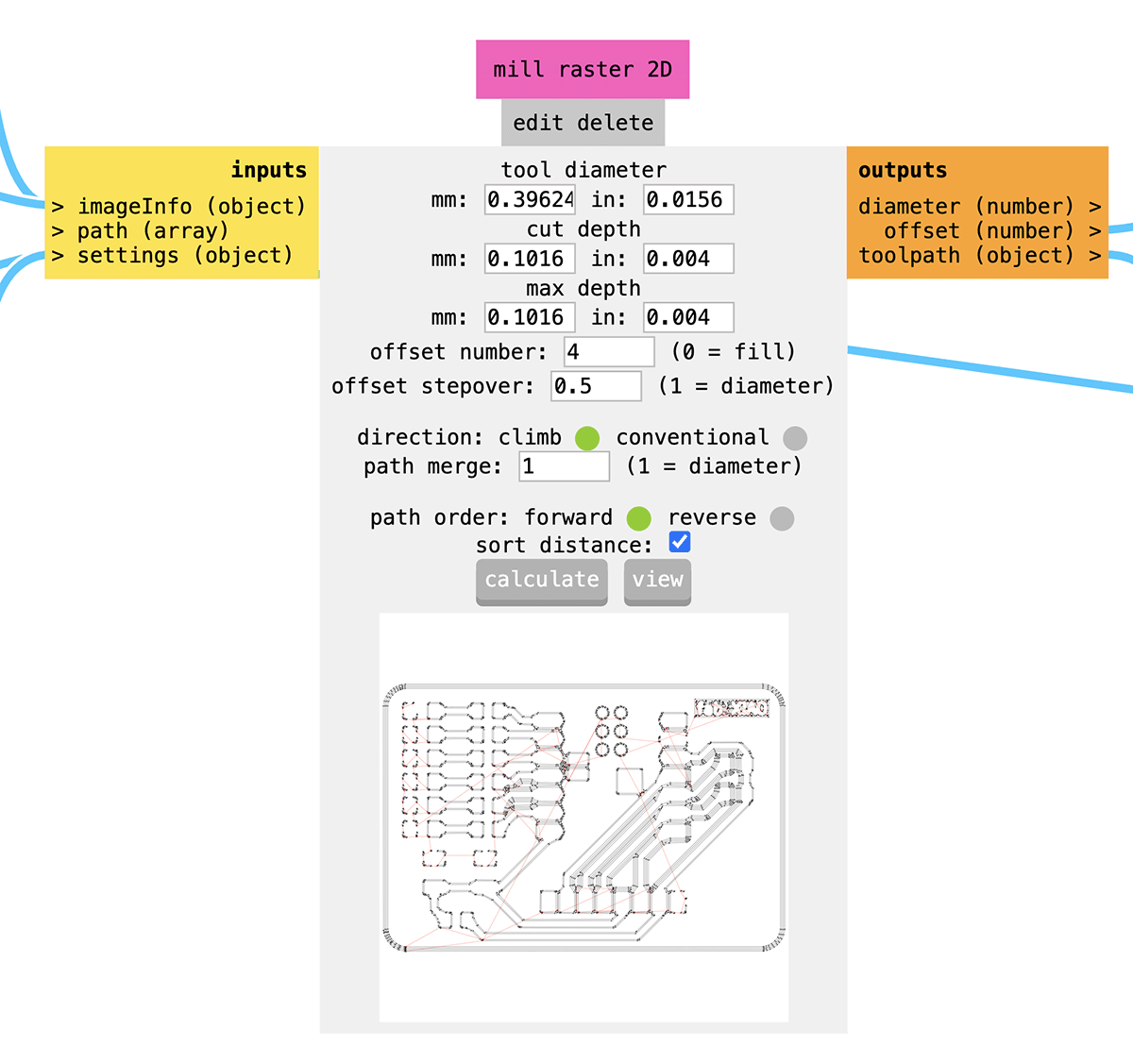
This interface shows the "mill raster 2D" module in MODs software, which is used to convert the previously imported PNG image into a tool path executable by the CNC mill. Here's a detailed explanation of the various parts and parameters of this interface:
Main Areas
Top Control Area
- mill raster 2D: Module name, used to convert bitmap (raster) images to milling paths
- edit delete: Edit or delete the current module
Left Input Area (Yellow)
- inputs: Input data label
- imageInfo (object): Image information imported from the previous step
- path (array): Defined path array
- settings (object): Configuration settings object
Right Output Area (Orange)
- outputs: Output data label
- diameter (number): Calculated tool diameter
- offset (number): Calculated offset
- toolpath (object): Generated tool path object, which will be sent to the CNC controller
Central Configuration Area (Gray)
Tool Settings
- tool diameter: Tool diameter, showing both millimeters (0.39624mm) and inches (0.0156 inch)
- This is a standard 1/64 inch end mill, used for PCB trace isolation
Cutting Depth Settings
- cut depth: Single-pass cutting depth, 0.1016mm (0.004 inch)
- Depth milled in each pass
- max depth: Maximum cutting depth, also 0.1016mm (0.004 inch)
- For trace isolation, usually only needs to cut deep enough to cut through the copper layer
Offset Settings
- offset number: 4: Number of offsets
- Value of 4 means 4 parallel cutting paths will be created, ensuring complete isolation of traces
- Note "(0 = fill)" indicates setting to 0 will perform fill milling
- offset stepover: 0.5: Offset step amount
- Value of 0.5 means adjacent paths overlap by 50%
- Note "(1 = diameter)" indicates setting to 1 means step amount equals tool diameter
Cutting Direction and Path Settings
- direction: Select milling direction
- climb: Selected, usually produces better cutting quality
- conventional: Not selected
- path merge: 1: Path merge threshold
- Value of 1 (equal to tool diameter) means paths less than tool diameter apart will be merged
- path order: Path order
- forward: Selected
- reverse: Not selected
- sort distance: Checked, indicates paths will be sorted by distance, reducing tool movement
Bottom Control Buttons
- calculate: Calculate tool path, will also immediately provide .nc file download upon completion
- view: View the calculated path
Bottom Preview Area
- Shows preview of calculated tool path
- Can see that the tool will move along the edges of the circuit board traces, creating isolation grooves
- The image shows the milling path for your XIAO extension board design
Working Principle
This module works as follows:
- Reads the imported PNG image (black areas indicate parts to be milled)
- Calculates milling paths based on the set parameters (tool size, cutting depth, etc.)
- Generates optimized tool movement trajectory (as shown by the lines in the image)
- These lines represent how the CNC machine will move the tool to create isolation grooves
In the preview image, you can see that the tool will mill along the edges of the circuit board traces, forming isolation grooves. Each line represents one tool pass, and multiple parallel lines (controlled by the offset number parameter) ensure the copper layer is completely cut to isolate the circuit.
After clicking "calculate", the system will generate detailed tool paths; clicking "view" allows you to preview these paths to ensure they match your design intent.
Parameter Testing and Recording
Since we are using the same equipment as the 2024 group, we referenced Matthew's document for parameter testing: CNC cutting, MCU development board making and testing.
Group Individual Assignment Cutting
Through Mods CE, we exported 2 .nc files, which were transferred via USB drive and loaded onto the Mach3 computer. The typical sequence is:
- First, install the 1/64 inch (0.4mm) V-shaped bit, load the trace isolation .nc file, set the origin in Mach3, and cut the traces, as shown below.
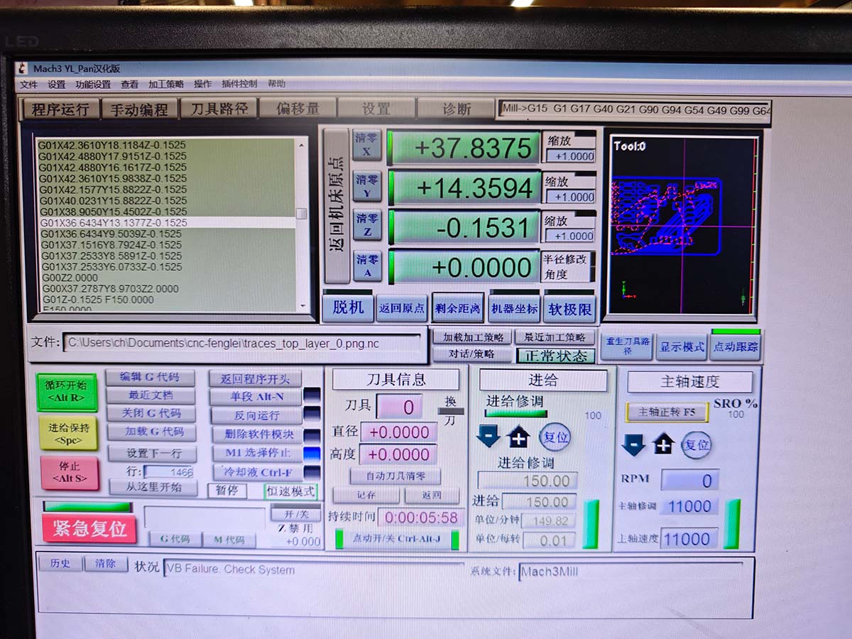
Mach3 cutting the trace file
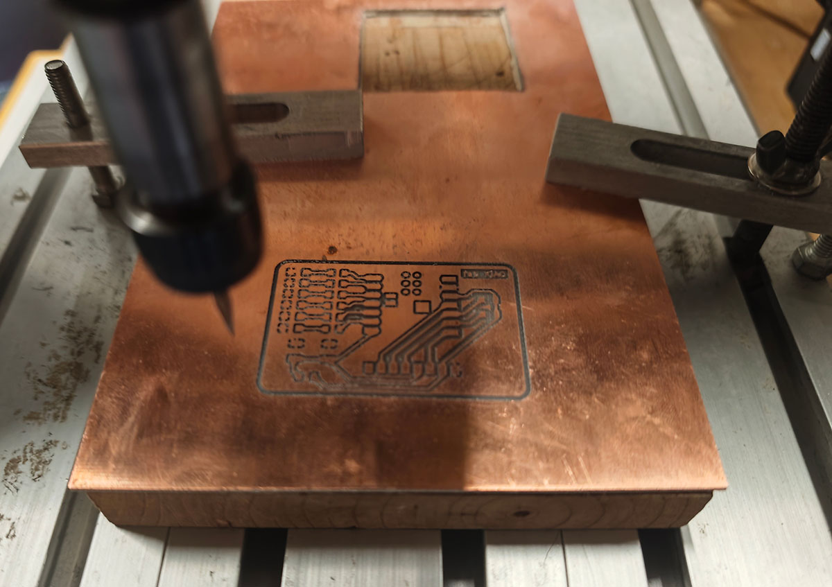
Completed trace cutting. After this step, remember not to move the board
- After completing the trace cutting, remember not to move the board, replace with the 1/32 inch (0.8mm) straight slot end mill, then load the outline cutting file and cut the outline.
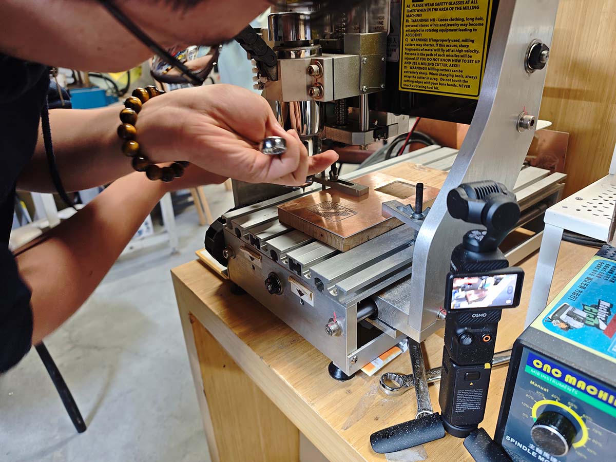
Replacing with the 1/32 inch (0.8mm) straight slot end mill
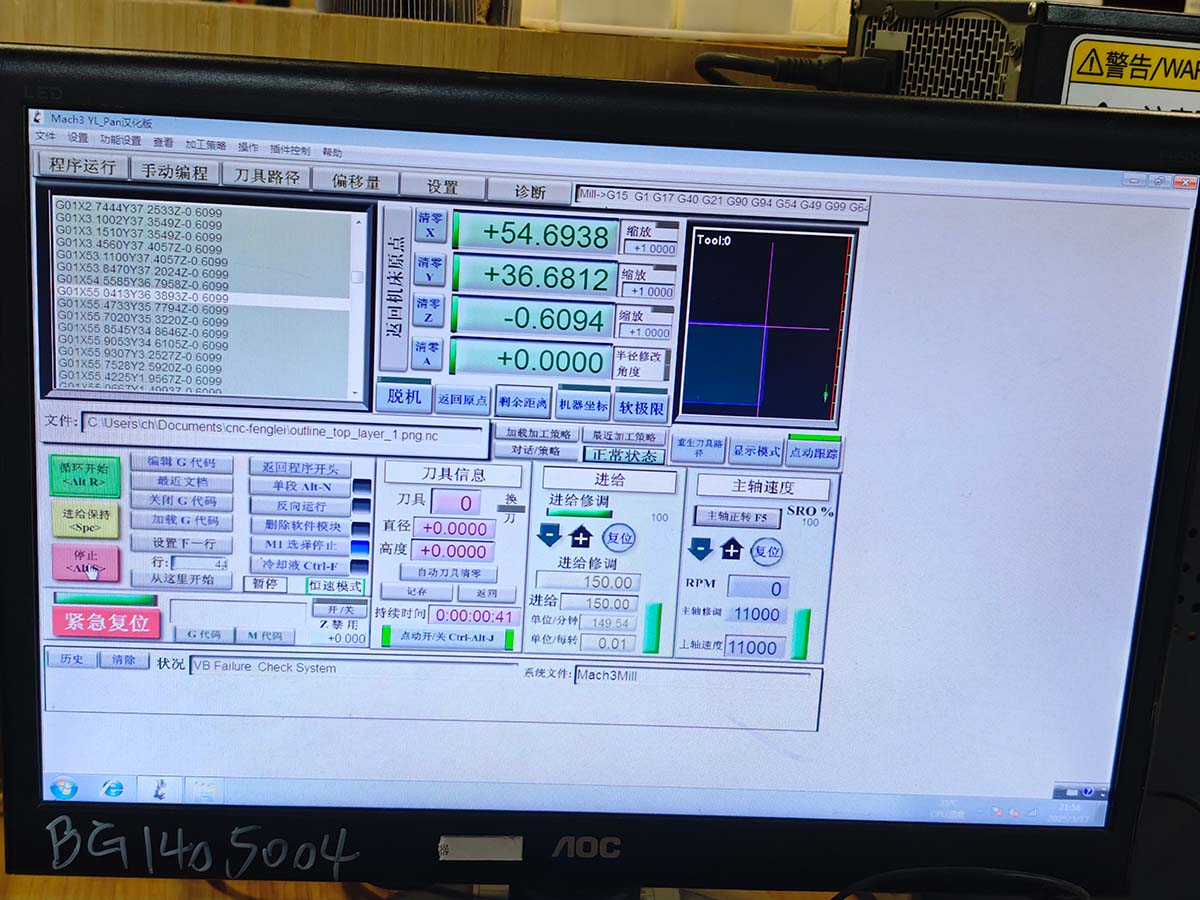
Loading the outline cutting .nc file
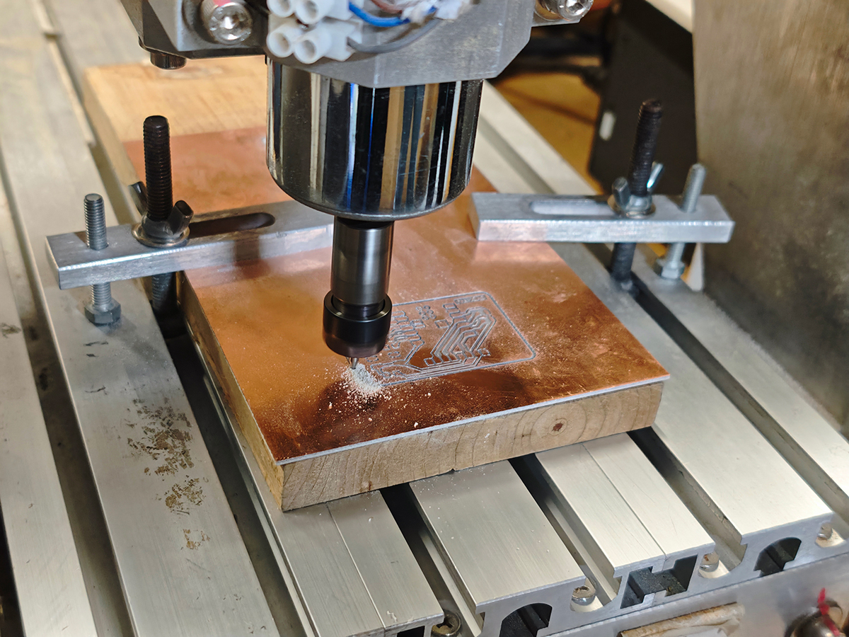
Cutting the outline is deeper and produces more debris
Hongtai Liu and I each completed our respective cutting work. Hongtai was concerned that his trace parts were too thin (he designed his PCB with 0.25mm wide traces), which would pose further challenges for soldering later. I designed with 0.5mm wide traces, which felt more friendly for milling PCB manufacturing.
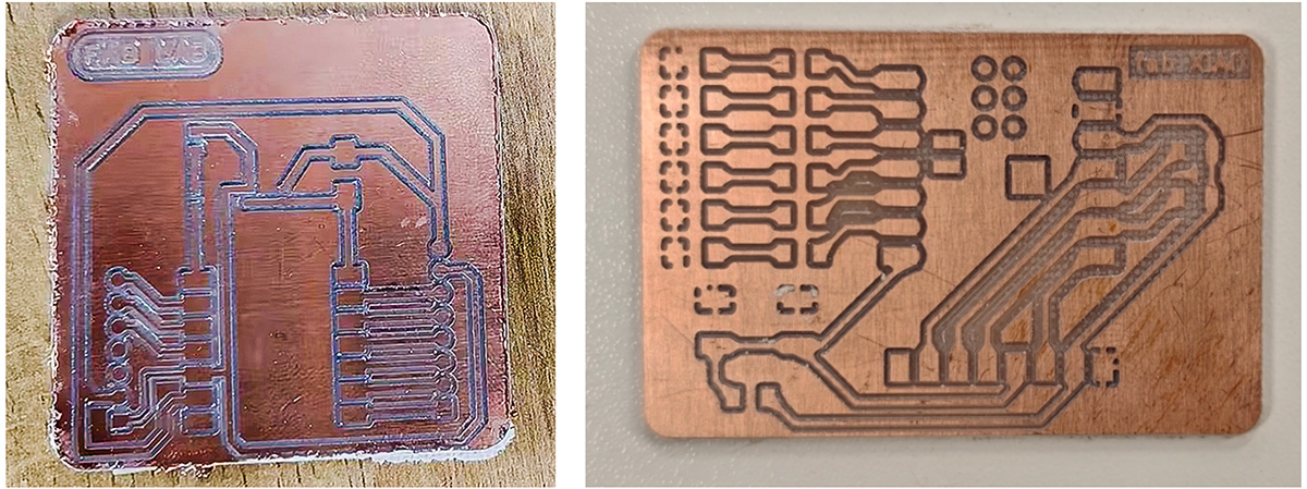
Hongtai's board on the left used 0.25mm trace width, which seemed too thin. I used 0.5mm trace width, which seemed more friendly for the milling process of PCB manufacturing
Challenges and Solutions
During this group assignment, we encountered several challenges, but successfully resolved them:
Equipment Connection Issues
On Friday night, we found that the computer driving the CNC would not power on. This computer had been in use for many years. After multiple attempts:
- On Saturday, team member Hongtai Liu purchased a USB-to-parallel port adapter, attempting to install CNC software on another computer, but the device still could not be recognized.
- On Monday morning, Chaihuo Makerspace administrator Li Jinhao replaced the power supply for the faulty computer, successfully resolving the computer startup issue. This cost us 2 valuable weekend days, directly resulting in insufficient time for soldering and documentation.
Equipment Startup Issues
On Monday evening, while training under Matthew's guidance, we still couldn't get the CNC machine to work. After a reminder from administrator Li Jinhao, we discovered the problem was with the emergency stop button:
The emergency stop button does not pop up automatically after being pressed and needs to be manually rotated to release, which is a safety design.
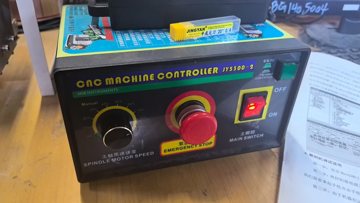
The red emergency stop button on the CNC machine. If the computer cannot connect to the CNC and the handwheel display is not lit, it's likely that this emergency stop button has not been released
After releasing the emergency stop button, the machine returned to normal working condition, allowing us to successfully complete the testing and cutting.
Experience Summary
Through this group assignment, we summarized the following key experiences:
- Pre-checks are important: Check power, connections, and emergency stop button status before using the equipment
- Parameter optimization is key: Different tools require different cutting parameters, requiring multiple tests to achieve the best effect
- Material fixation must be secure: PCB boards can warp during cutting, requiring both double-sided tape and fixing plates simultaneously
- Tool selection affects quality: V-shaped bits work better for cutting traces, while straight slot end mills are suitable for cutting outlines
- Cleaning and maintenance: Clean the equipment promptly after cutting to extend tool life
Reference Resources
Submitting Designs to PCB Manufacturers: JLCPCB Experience Sharing
This article records the complete process of submitting PCB designs to JLCPCB, as a result of the Week 8 Electronics Production course group assignment. Through this practice, we mastered the entire process from design to submission, ordering, review, and final production, accumulating valuable experience for future PCB production.
Preparation
Design File Preparation
In Week 6's assignment, I designed an extension board based on XIAO ESP32C3.
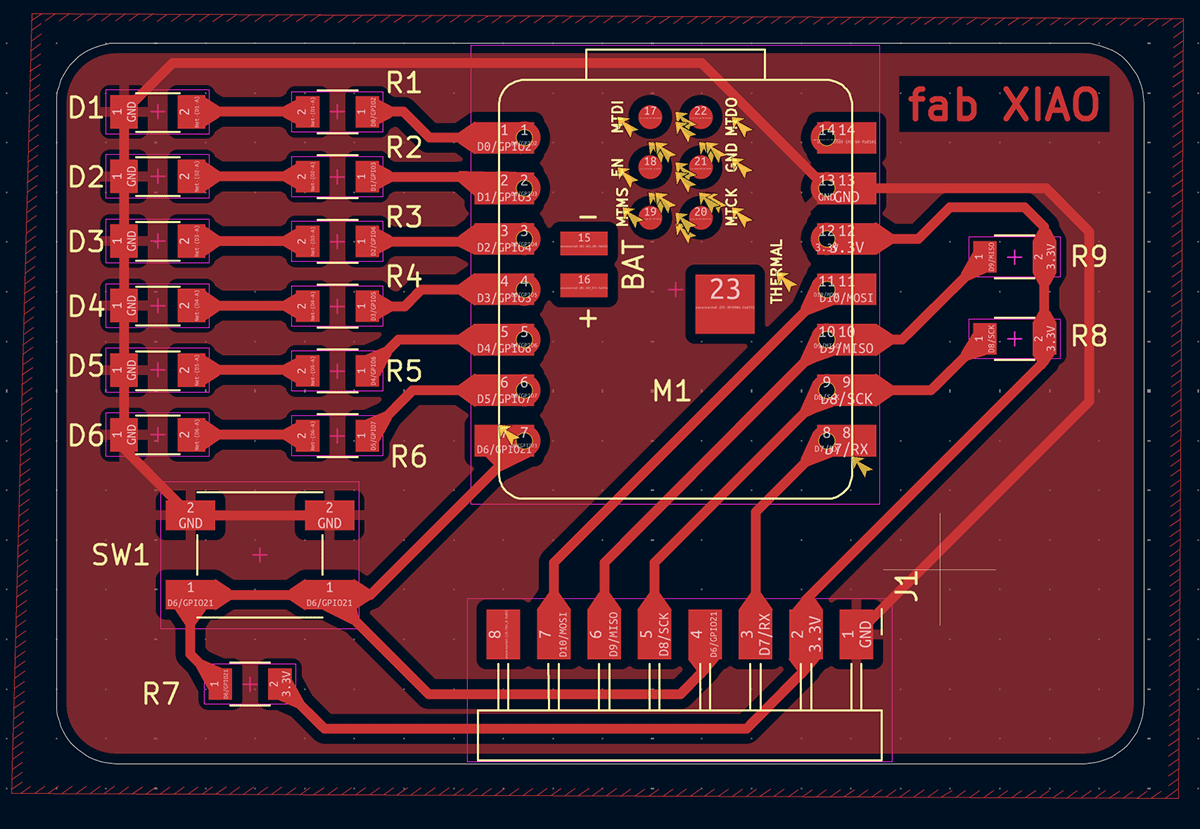
PCB design file prepared during Week 6 individual assignment
After completing the design, I needed to export Gerber files for manufacturing. Initially, I only prepared the following Gerber files through KiCAD's top menu "File > Manufacturing output > Gerbers (.gbr)":
XIAO_ESP32C3_Extension_CNC2-F_Cu.gbr- Top copper layerXIAO_ESP32C3_Extension_CNC2-Edge_Cuts.gbr- Board outline
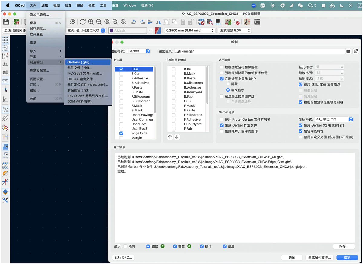
First attempt at manufacturing output, providing only the F_Cu and Edge_Cuts layers
2.2 Learning Points
This practice made me understand that complete PCB manufacturing files must include more content. Through communication with the manufacturer and self-learning, I supplemented the following necessary files:
XIAO_ESP32C3_Extension_CNC2-B_Mask.gbr- Drill fileXIAO_ESP32C3_Extension_CNC2-F_Mask.gbr- Solder mask layerXIAO_ESP32C3_Extension_CNC2-F_Silkscreen.gbr- Silkscreen layer
This experience taught me that in commercial PCB manufacturing, complete file preparation is crucial for smooth production.
Submission and Ordering Process
PCB Board Ordering
On the afternoon of March 15, 2025, I chose JLCPCB as the PCB manufacturer and began attempting to order PCB boards. Here are the detailed ordering steps:
- Enter the JLCPCB online ordering platform.

JLCPCB manufacturing homepage
- Select basic parameters:
- Board material category: FR-4
- Board size: 5.48 × 3.63 cm
- Board quantity: 5 pieces
- Board layers: 1 layer
- Finished board thickness: 1.0mm
- Application industry: Consumer electronics
- Product type: Economic type
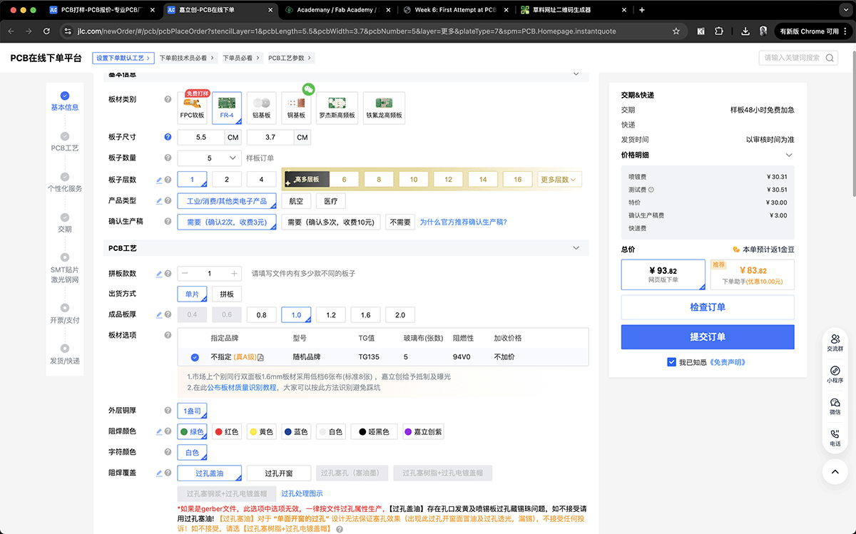
The PCB online ordering options are numerous, and it can be a bit confusing the first time
- Upload Gerber files: Submit the zip package of prepared Gerber files (the JLCPCB platform only allows uploading zip or rar compressed packages).
Initially, I thought I only needed to provide these 2 files:
XIAO_ESP32C3_Extension_CNC2-F_Cu.gbr- Top copper layerXIAO_ESP32C3_Extension_CNC2-Edge_Cuts.gbr- Board outline
- Wait for technical review: The system automatically checks the files.
Technical Review
I initially thought there would be no problems, but after dinner, I received a call from a JLCPCB employee saying my technical review had failed: I was missing necessary drill, solder mask, and silkscreen files. I didn't know what a solder mask was, so I asked the JLCPCB employee. The employee said without this file, soldering would be impossible. So I quickly learned about this part.
Basic Knowledge of Essential PCB Manufacturing Files
Drill File
- Function: Defines the position, size, and type of all holes on the PCB board
- File format: Usually in Excellon format (.drl) or Gerber format (.gbr)
- Hole types:
- Through Hole: Holes connecting the top and bottom layers of the PCB
- Mounting Hole: Holes used for fixing the PCB
- Via: Electrical connections connecting different copper layers
- Importance: Accurate drill files ensure components can be correctly installed and electrical connections are reliable
Since my board was designed for single-sided surface mount, I didn't consider the drill hole issue and didn't output drill files. If your project needs to output drill files, you can find it under "File > Manufacturing output > Drill files (.drl)" in the top menu.
Solder Mask Layer File
- Function: Defines areas on the PCB that do not need to be covered with solder mask ink, usually pads and test points
- File format: Gerber format, usually named
*_Mask.gbr- Purpose:
- Protects copper foil from oxidation
- Prevents short circuits during soldering
- Improves electrical insulation
- Forms openings at pads for soldering
- Importance: Without correct solder mask layer, the PCB will be difficult to solder or may short circuit during use
I found the
F.Masklayer in the PCB appearance layer in KiCAD, as shown below. If this layer is not output to the manufacturer, the entire PCB will be covered with solder mask ink that protects the circuit, making it impossible to solder components.
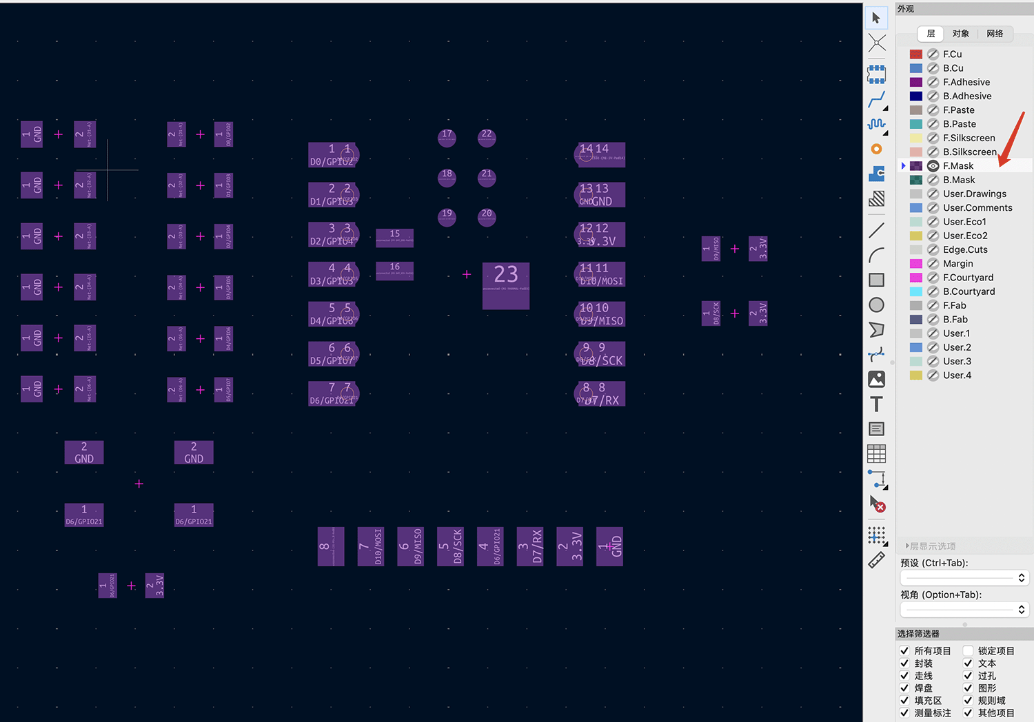
F.Masklayer represents the top solder mask layer
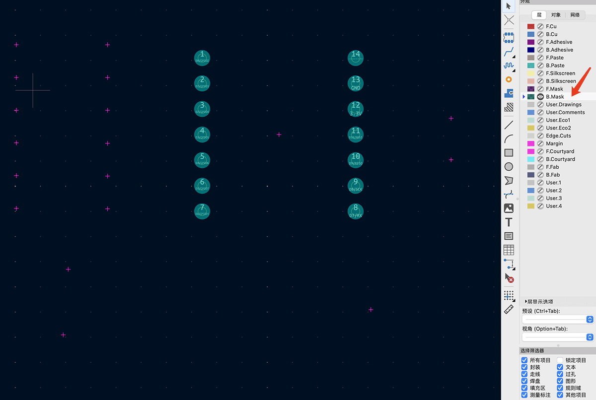
B.Masklayer represents the bottom solder mask layerSilkscreen Layer File
- Function: Defines text, markings, patterns, and identifiers on the PCB surface
- File format: Gerber format, usually named
*_Silkscreen.gbr- Common content:
- Component identifiers and numbers (such as R1, C3, U2, etc.)
- Polarity markings (such as positive and negative poles of capacitors, diodes)
- Connector pin numbering
- Warning signs and logos
- Version numbers and dates
- Importance: Silkscreen helps identify component positions, facilitating assembly, debugging, and maintenance
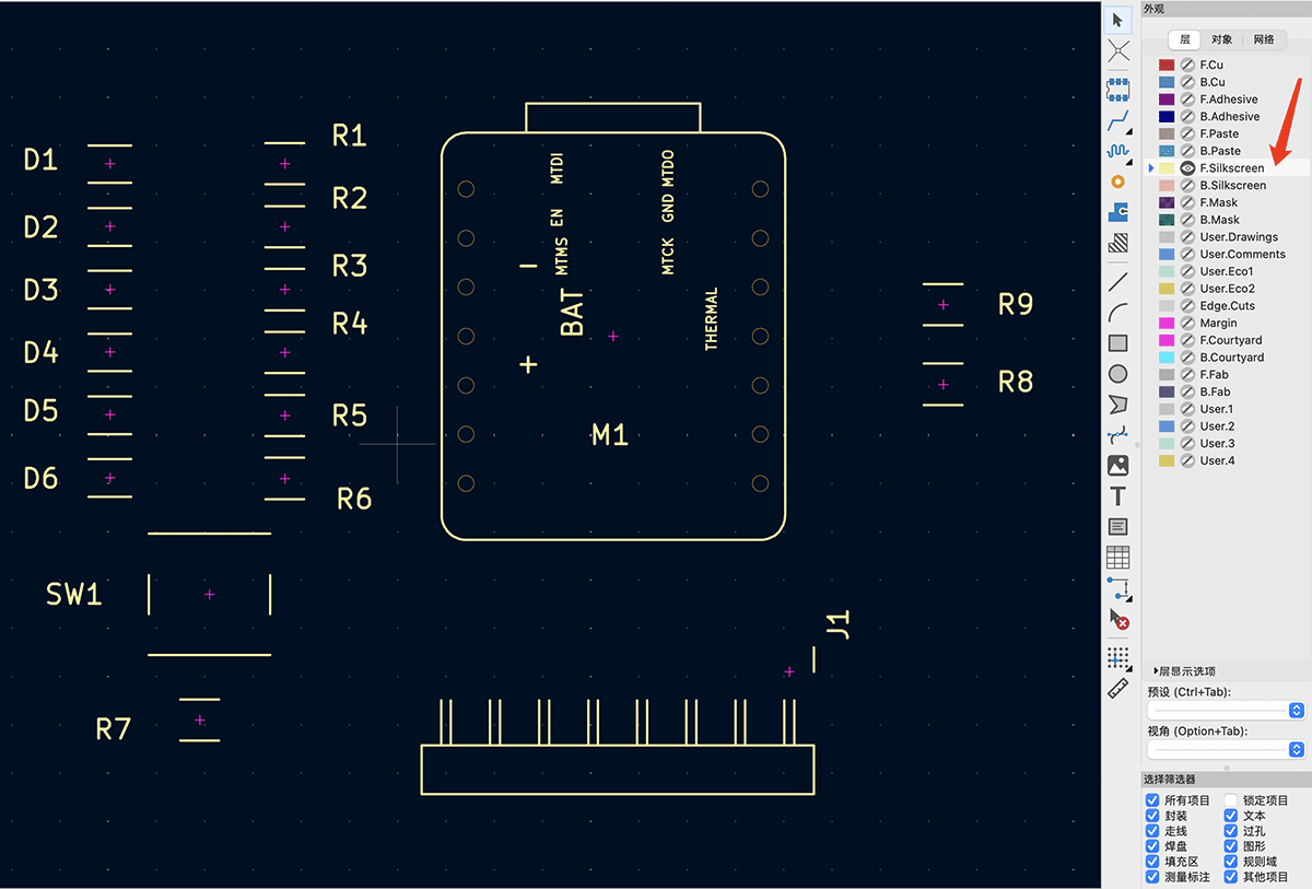
F.Silkscreen layer represents the top silkscreen content
After learning this, I re-exported the following layers from KiCAD's top menu "File > Manufacturing output > Gerbers(.gbr)": F.Cu, F.Silkscreen, F.Mask, B.Mask, Edge.Cuts.
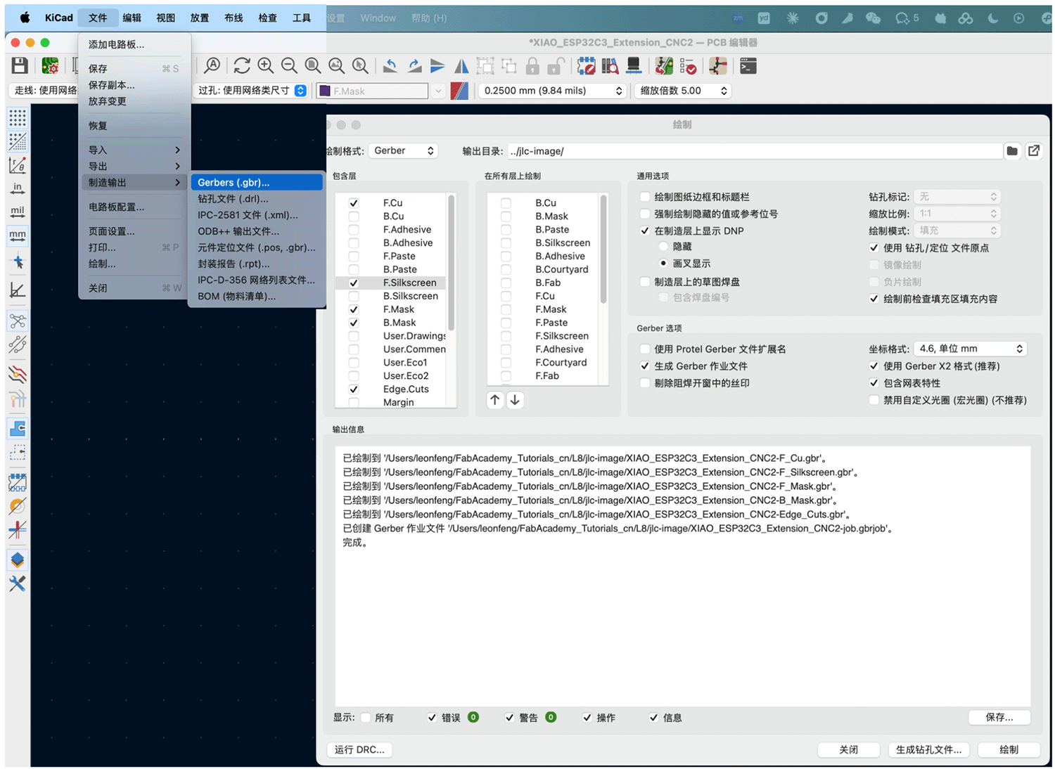
Second time re-exporting through KiCAD's manufacturing output Gerbers(.gbr)
File Preparation Considerations
- Alignment precision: All layer files must be perfectly aligned
- Hole diameter standardization: Drill hole dimensions should follow the manufacturer's capability range
- Solder mask opening: Solder mask openings around pads are usually slightly larger than the pads (expanded by 2-3mil)
- Silkscreen position: Avoid silkscreen text covering pad areas
- File naming: Follow standard naming conventions for easy manufacturer identification
A complete PCB manufacturing file set typically includes copper layers, solder mask layers, silkscreen layers, drill files, and board outline files. These files collectively define the physical characteristics and manufacturing requirements of the PCB. Missing any critical file can lead to manufacturing problems or review failure.

After packaging the exported .gbr files into a zip file, I submitted them again
After supplementing the files and resubmitting, the review passed and entered the production process. This process taught me the complete file system required for PCB manufacturing.
SMT Service Evaluation
In addition to basic PCB manufacturing, I also explored SMT assembly services. SMT online ordering requires providing BOM and coordinate lists, as shown below.
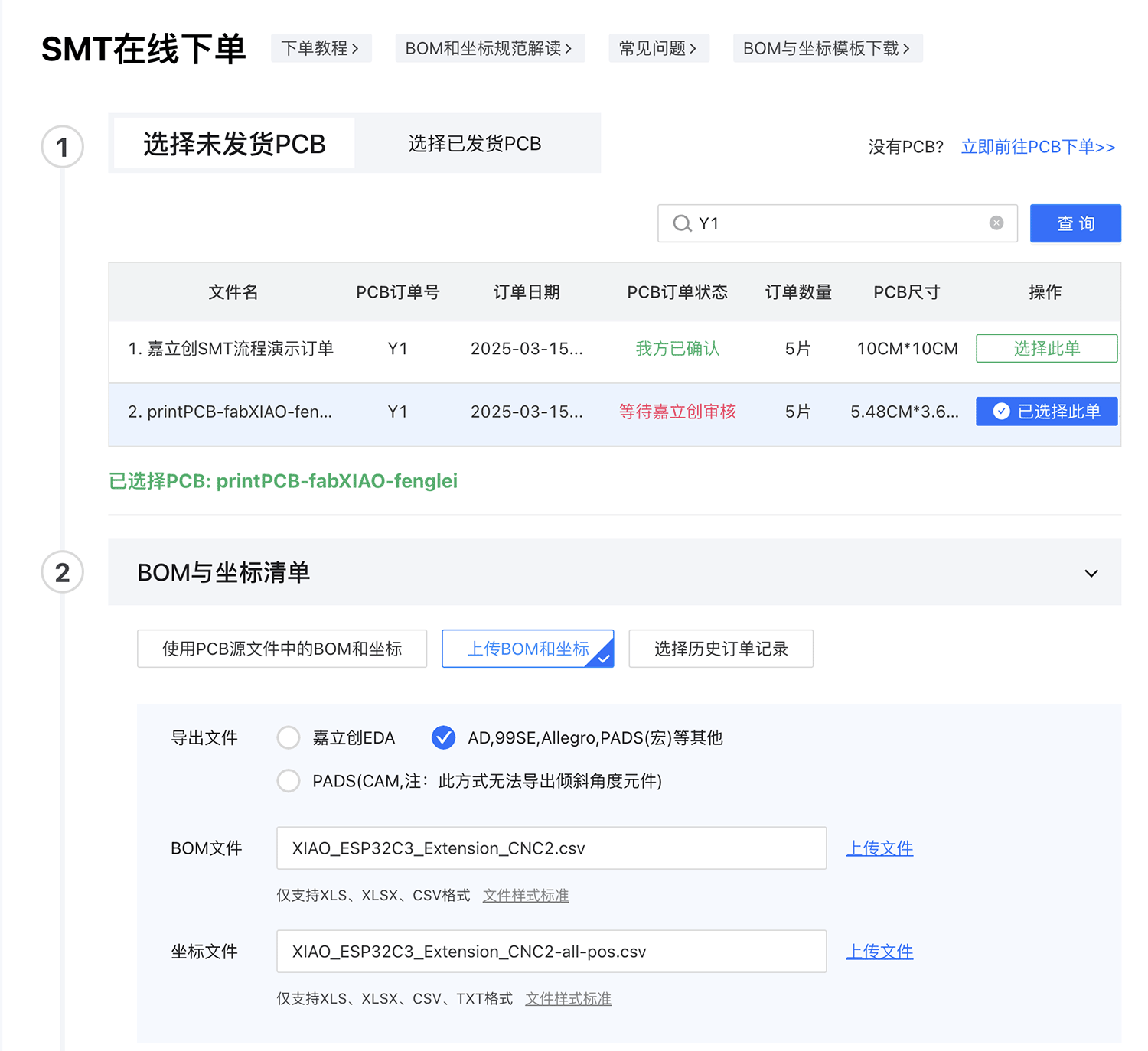
SMT online ordering requires providing BOM and coordinate lists
- Upload BOM and coordinate files, which can be found under "File > Manufacturing output" in KiCAD's top menu. For the component positioning file, I chose CSV format, as shown below.
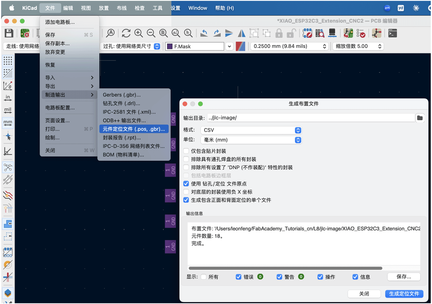
The positioning file content is as follows.
Ref,Val,Package,PosX,PosY,Rot,Side
"D1","LED_1206","LED_1206",150.100000,-85.950000,0.000000,top
"D2","LED_1206","LED_1206",150.100000,-89.200000,0.000000,top
"D3","LED_1206","LED_1206",150.100000,-92.450000,0.000000,top
"D4","LED_1206","LED_1206",150.100000,-95.700000,0.000000,top
"D5","LED_1206","LED_1206",150.100000,-98.950000,0.000000,top
"D6","LED_1206","LED_1206",150.100000,-102.200000,0.000000,top
"J1","PinHeader_01x08_P2.54mm_Horizontal_SMD","PinHeader_01x08_P2.54mm_Horizontal_SMD",185.280000,-112.250000,-90.000000,top
"M1","Module_XIAO-ESP32C3","SeeedStudio_XIAO_ESP32C3",176.165000,-94.880000,0.000000,top
"R1","R_1206","R_1206",159.150000,-85.950000,180.000000,top
"R2","R_1206","R_1206",159.150000,-89.210000,180.000000,top
"R3","R_1206","R_1206",159.150000,-92.470000,180.000000,top
"R4","R_1206","R_1206",159.150000,-95.730000,180.000000,top
"R5","R_1206","R_1206",159.150000,-98.990000,180.000000,top
"R6","R_1206","R_1206",159.150000,-102.250000,180.000000,top
"R7","R_1206","R_1206",154.750000,-114.750000,0.000000,top
"R8","R_1206","R_1206",193.250000,-97.375000,0.000000,top
"R9","R_1206","R_1206",193.250000,-93.250000,0.000000,top
"SW1","Switch_Tactile_Omron","Button_Omron_B3SN_6.0x6.0mm",155.250000,-108.250000,180.000000,top
JLCPCB has format requirements for positioning files. The field names need to be consistent with their documentation standards, otherwise they cannot be recognized. So I modified the field names in the positioning CSV file.
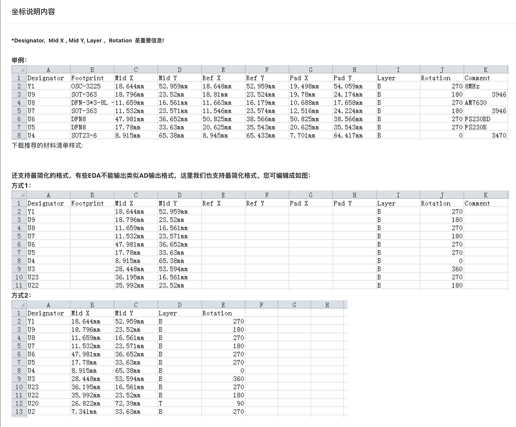
Coordinate file example provided by JLCPCB
- The system automatically matches available components, but indicated that my BOM file had low matching, with most requiring manual selection of components from JLCPCB's component library.
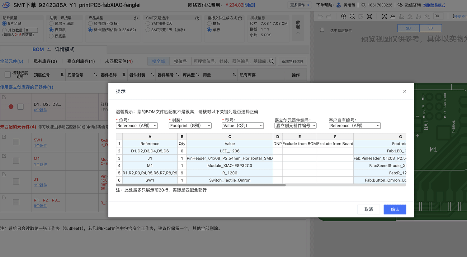
My BOM file had low matching
- The XIAO ESP32S3 module could not be directly provided through JLCPCB and could only be marked as an unmounted component. The interface allowed real-time preview of the post-assembly effect, as shown below.
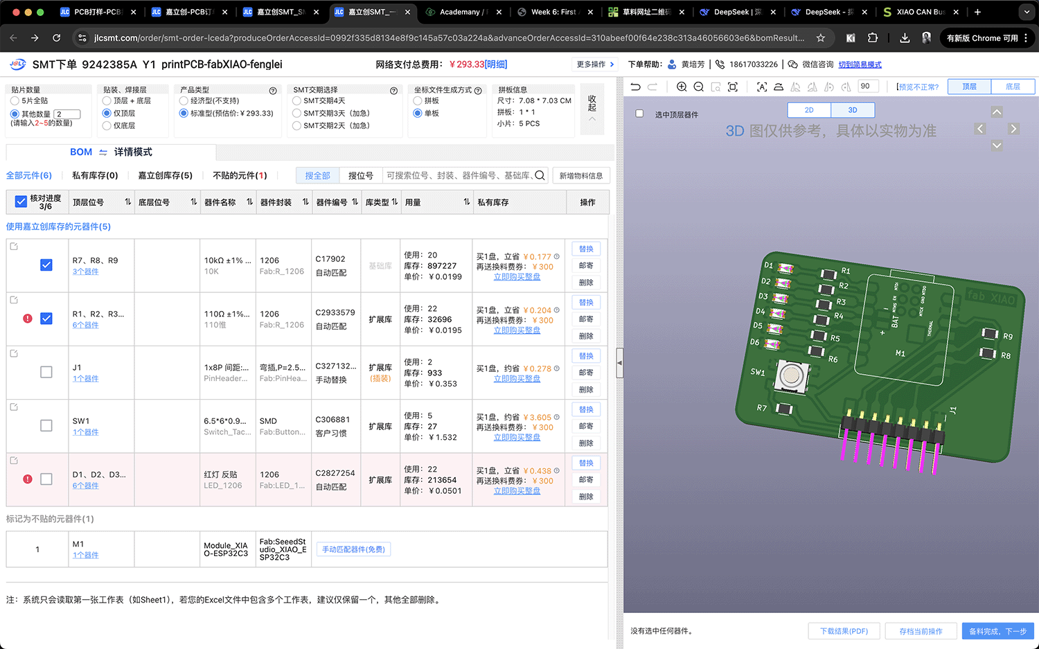
Replace unmatched components and view the effect after assembly
The final quote for assembling 2 boards was about 304.33 yuan, as shown below. Considering the feasibility and economics of self-soldering, I ultimately chose to only manufacture the PCB boards.
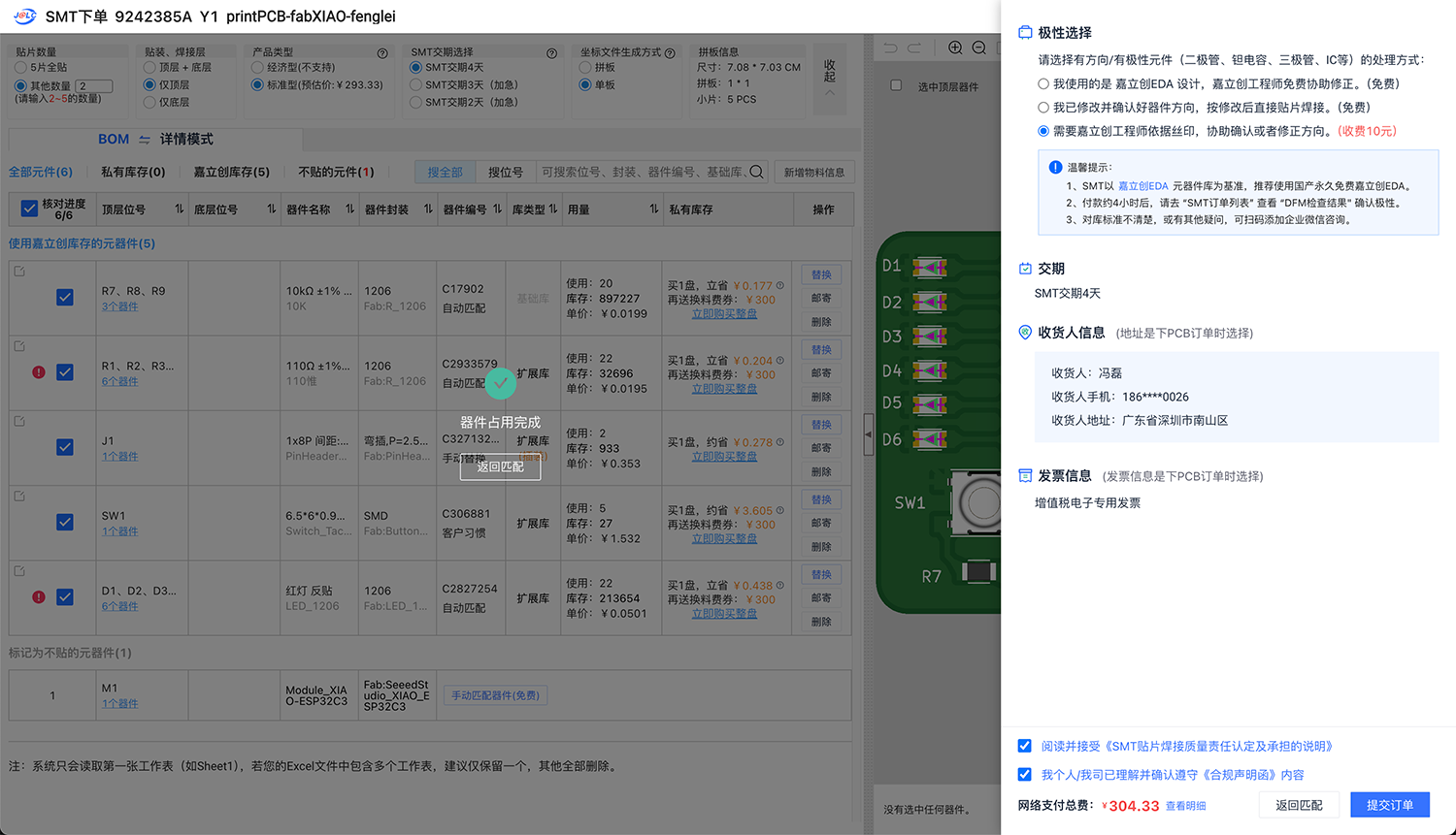
JLCPCB's price for assembling 2 boards is 304.33 yuan
Price Analysis
PCB Manufacturing Price
The final confirmed PCB manufacturing order price details:
- Base price: 104.49 yuan
- Quantity: 5 single-sided boards
- Cost per board: approximately 20.90 yuan
Price breakdown:
- Testing fee: 30.51 yuan
- Material fee: 30.00 yuan
- Confirmation production fee: 3.00 yuan
- Other fees: 40.98 yuan
SMT Assembly Price Evaluation
Although I did not ultimately choose the SMT assembly service, I received the following quote:
- Total SMT assembly price: approximately 304.33 yuan
- Assembly quantity: 2 pieces (remaining 3 pieces as backup)
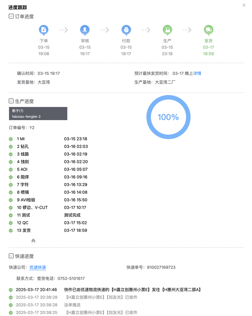
Production Progress Tracking
The JLCPCB platform provides detailed production progress tracking. My order went through the following production steps:
- Order: 03-15 19:08
- Review: 03-15 19:17
- Payment: 03-15 19:17
- Production: 03-15 23:18
- Shipping: 03-17 18:59
| 1 MI | 03-15 23:18 |
|---|---|
| 2 Drilling | 03-16 02:03 |
| 3 Circuit | 03-16 02:19 |
| 4 Etching | 03-16 02:20 |
| 5 AOI | 03-16 05:07 |
| 6 Solder mask | 03-16 09:16 |
| 7 Character | 03-16 13:29 |
| 8 Spray tin | 03-16 14:08 |
| 9 AVI inspection | 03-16 15:50 |
| 10 Edge cutting, V-CUT | 03-17 10:17 |
| 11 Testing | Testing completed |
| 12 QC | 03-17 15:02 |
| 13 Shipping | 03-17 18:59 |
Ordered on 03-15 19:08, shipped on 03-17 18:59. On the morning of March 18, I received the PCB boards I designed. This might be one of the benefits of living in Shenzhen. If you're willing to pay more, this time could be even shorter.
On the morning of March 18, I received the manufactured PCBs. I was very excited to receive the first batch of "mass-produced" PCBs I had designed.
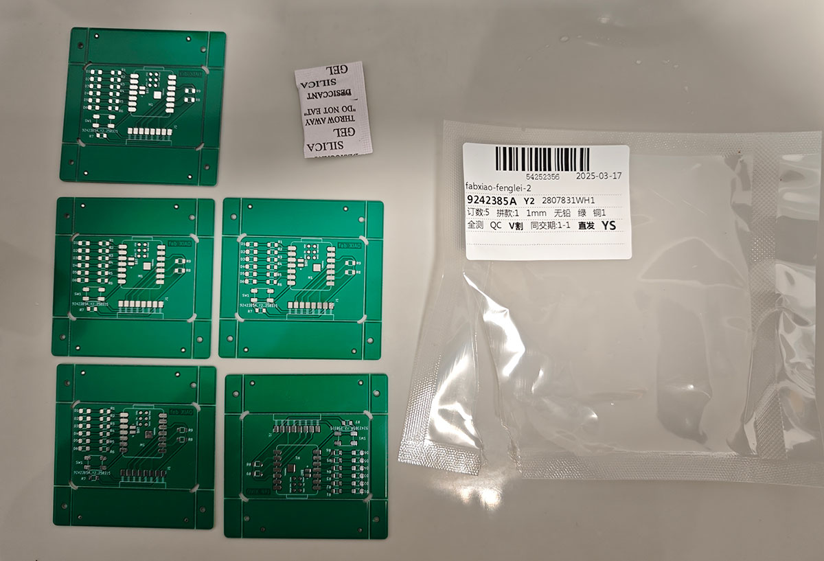
5 PCB boards sealed with packaging, with desiccant included
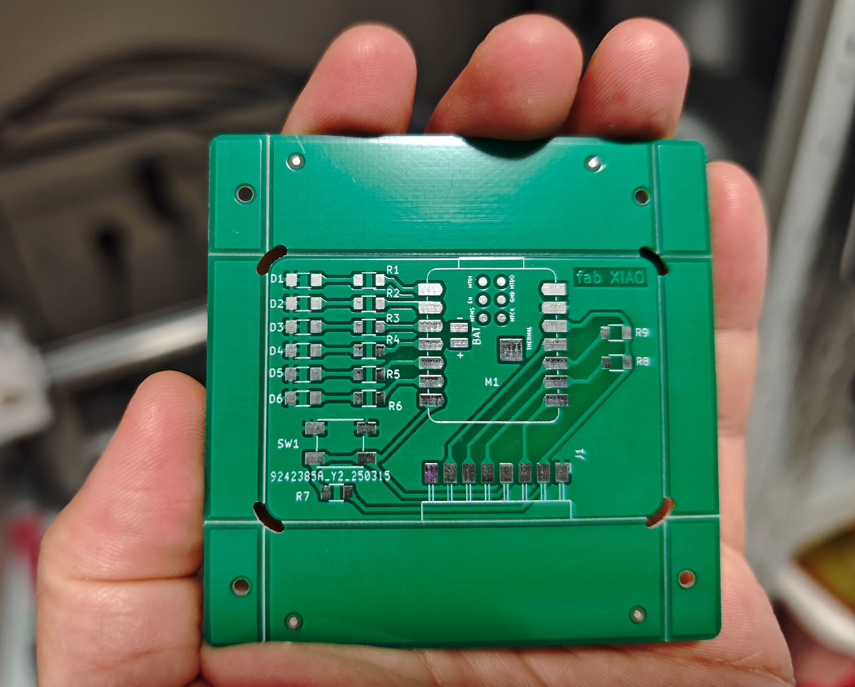
The boards have cutting lines and can be broken apart by hand
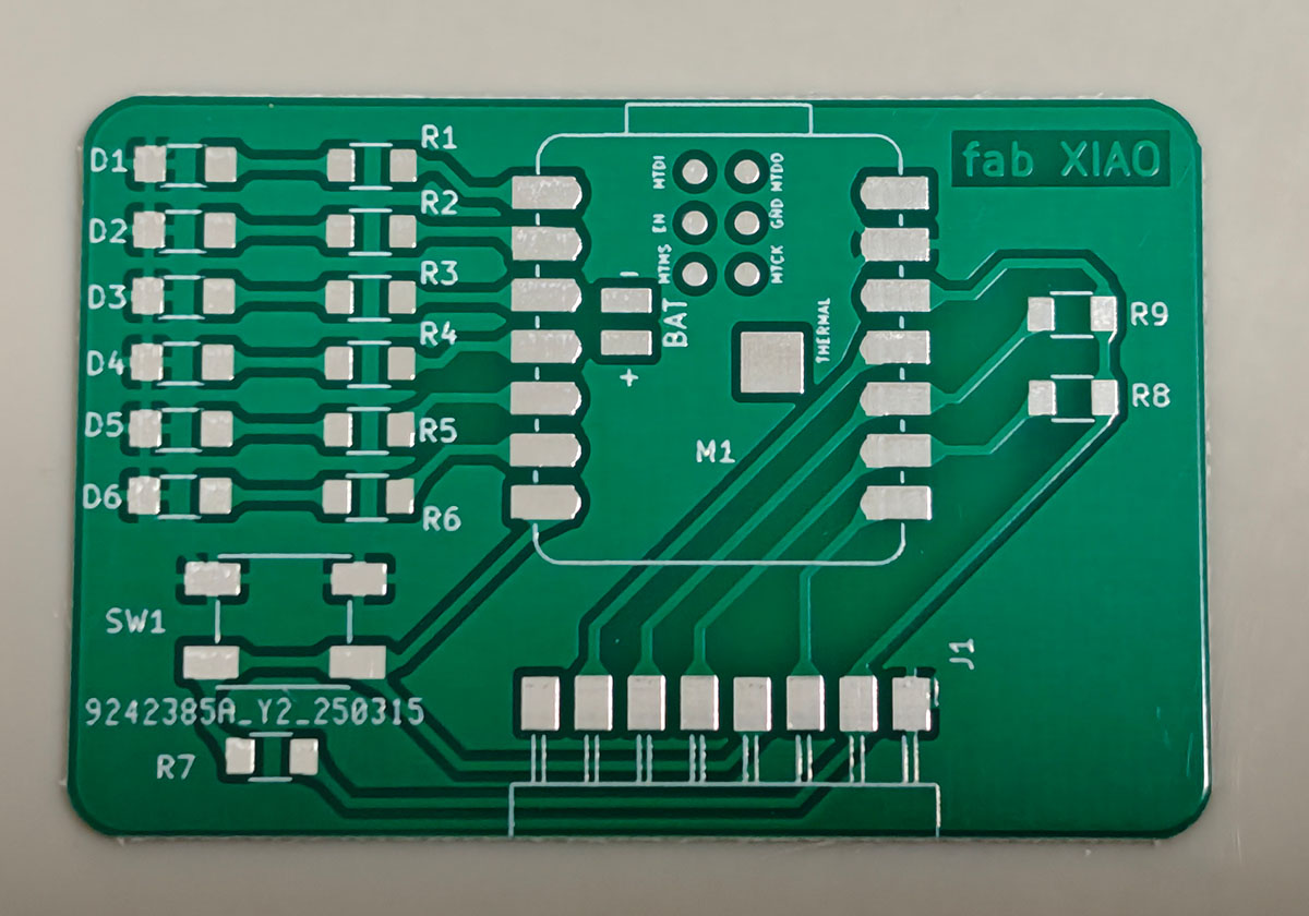
The manufacturing quality feels perfect
6. Experience and Lessons
6.1 File Preparation Experience
- Completeness is crucial: PCB manufacturing requires a complete set of files, including copper layers, drill holes, solder mask, silkscreen, etc.
- Format standardization: Manufacturers typically require standard Gerber format files
- Pre-check: Before submission, use a Gerber viewer to check the completeness and correctness of files
6.2 Manufacturer Selection Experience
- Technical support: JLCPCB provided timely technical support, proactively contacting me when files were incomplete
- Price transparency: The platform provided detailed price breakdown
- Full-process service: One-stop service from PCB manufacturing to component assembly is very convenient
7. Conclusion
Through this practice of submitting PCB designs to JLCPCB, I gained first-hand experience with commercial PCB manufacturing. This process not only completed the course assignment requirements but, more importantly, helped me understand the complete workflow from design to physical production.
This experience particularly emphasized the importance of preparing complete manufacturing files and the necessity of good communication with manufacturers. Ultimately, I successfully obtained 5 high-quality PCB boards, laying the foundation for subsequent assembly and testing.
The online platform provided by the manufacturer greatly simplified the ordering process, and detailed production progress tracking also provided a good user experience. These tools and services are very valuable for rapid prototype development and small-batch production.
8. References
- JLCPCB online ordering platform: https://www.jlc.com/
- Gerber file format specification: http://www.gerber-format.com/
- PCB manufacturing process: https://www.jlc.com/portal/vtechnology.html