1. Electronics Design
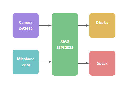
This week, I worked on the electronics design process for the Smart Glasses Kit, which is part of my final project. The kit is powered by the XIAO ESP32S3 as the main controller. The design includes a display module and an audio output module, ensuring a compact yet functional layout.
The schematic and PCB were developed using 嘉立创EDA.
1.1 Design Steps
1.1.1 Defining Requirements
Before starting the design, I outlined the key hardware requirements:
-
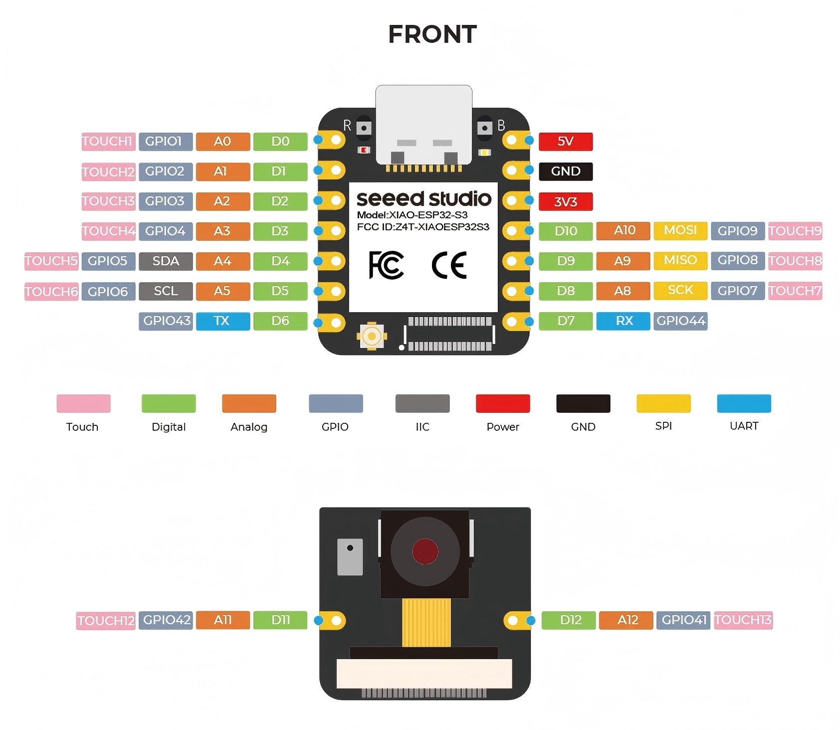
Microcontroller: XIAO ESP32S3
- Compact and powerful with Wi-Fi and Bluetooth capabilities
- Suitable for handling display and audio processing tasks
-
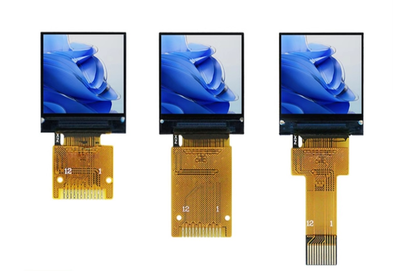
Display Module: GAC901 128x128 LCD
- Small form factor suitable for wearable devices
- Uses SPI communication for efficiency
-
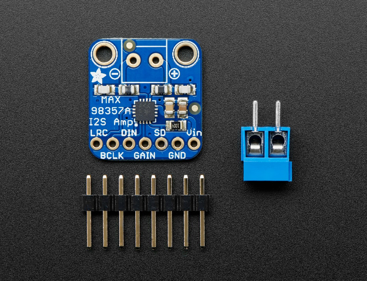
Audio Output Module: MAX98357A
- I2S digital audio amplifier
- Provides clear and efficient audio output
With these requirements in mind, I proceeded with the schematic design.
1.1.2 Schematic Design
I used 嘉立创EDA to design the schematic, ensuring that all components were properly connected and optimized for performance.
1.1.2.1 Microcontroller
The first step was to add the XIAO ESP32S3 microcontroller pinout to the schematic.
-
Connector: 1x7 2.54mm Pitch
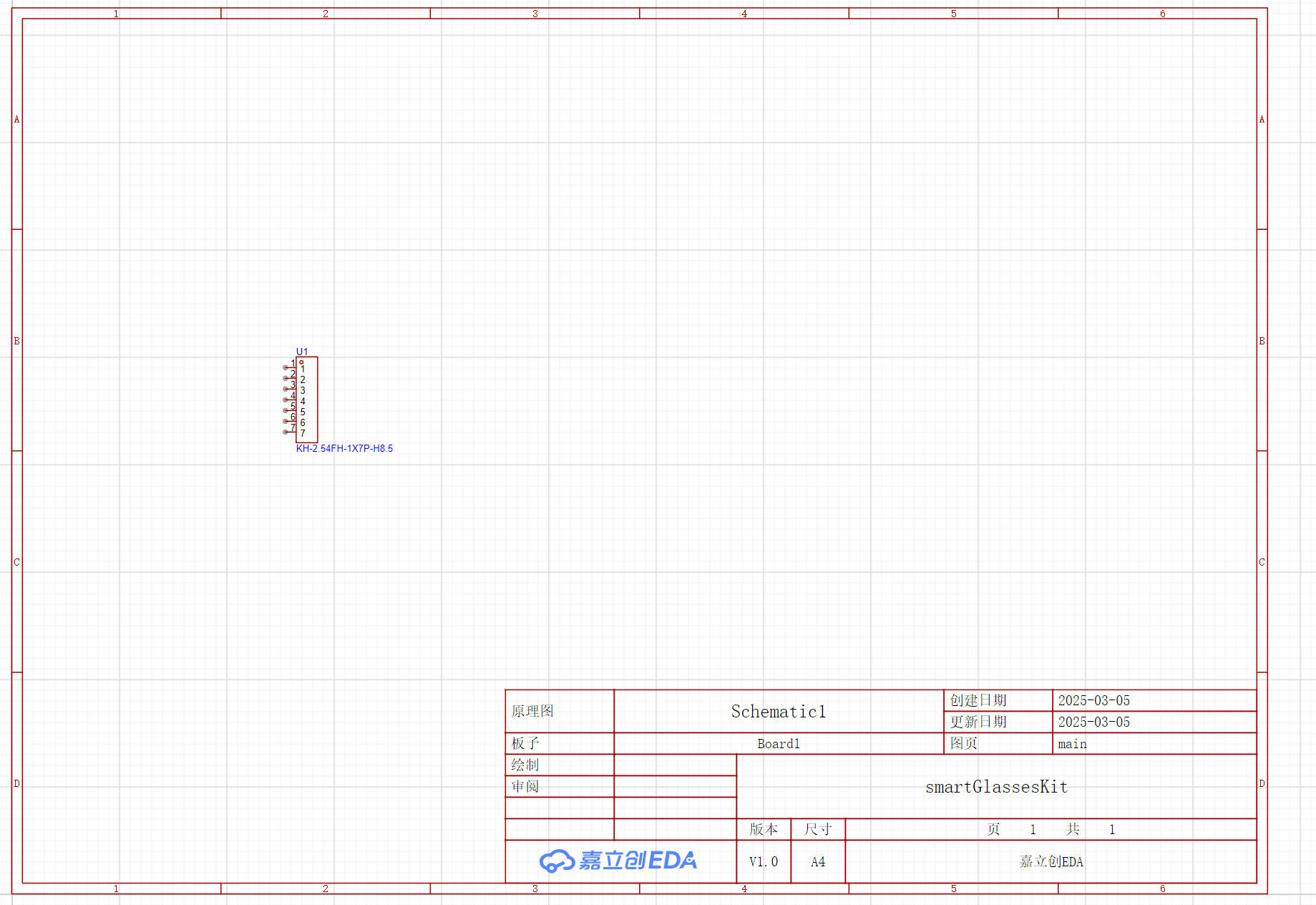
Next, I assigned pin nets to ensure proper connectivity:
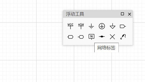
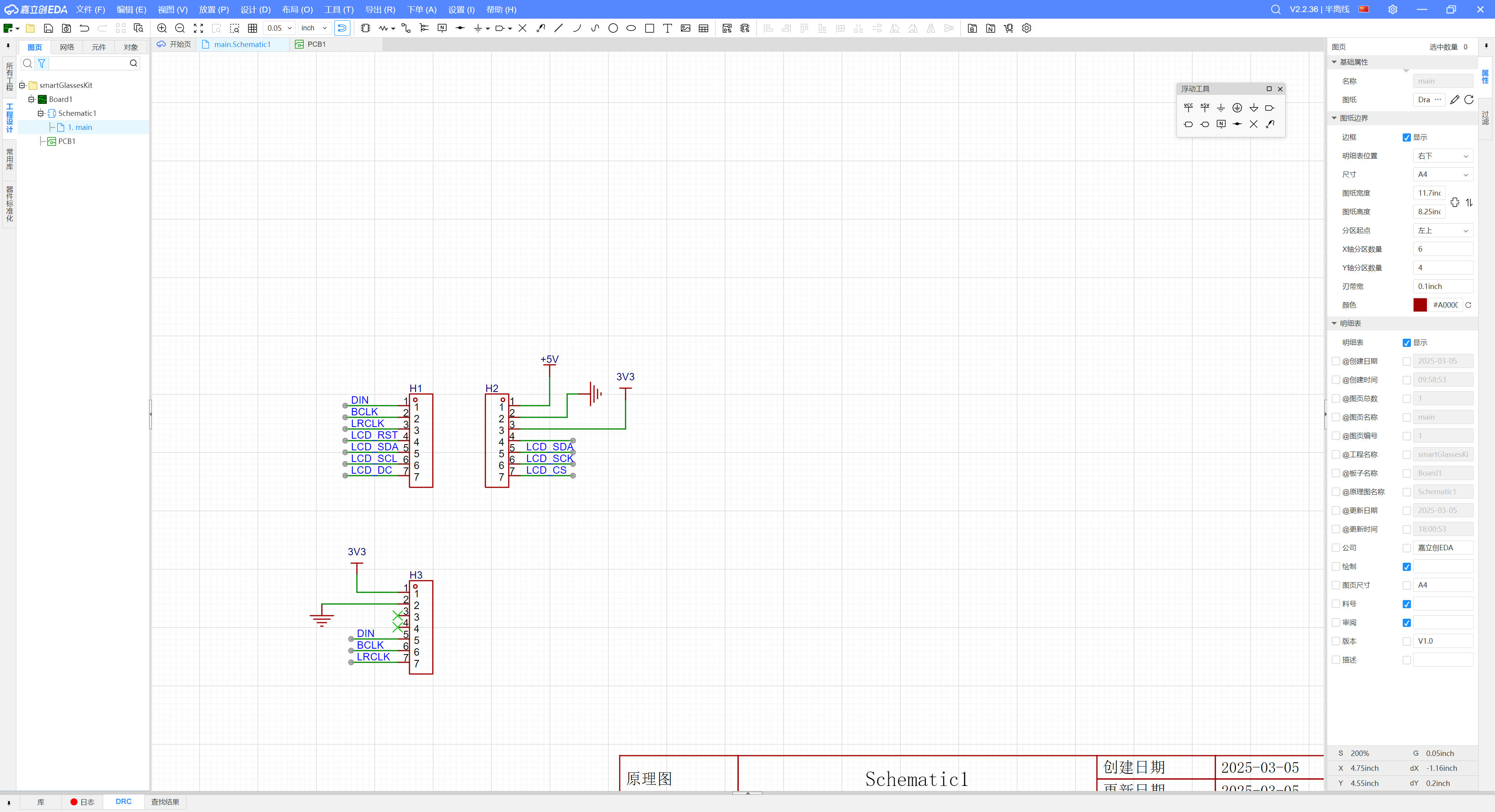
Here is the completed wiring of the microcontroller:
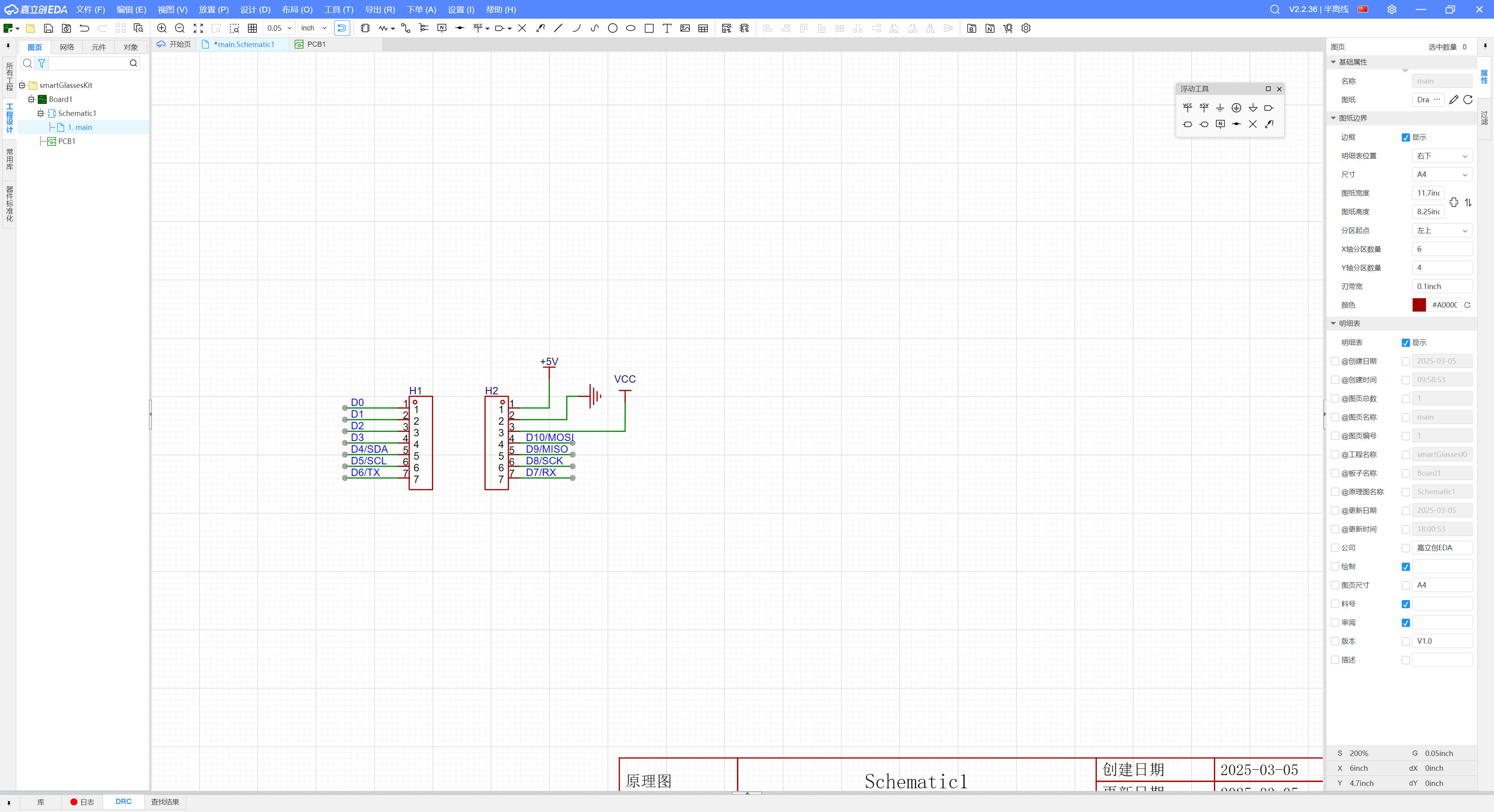
1.1.2.2 Audio Output Module
The next step was to integrate the MAX98357A audio output module.
-
Connector: 1x7 2.54mm Pitch
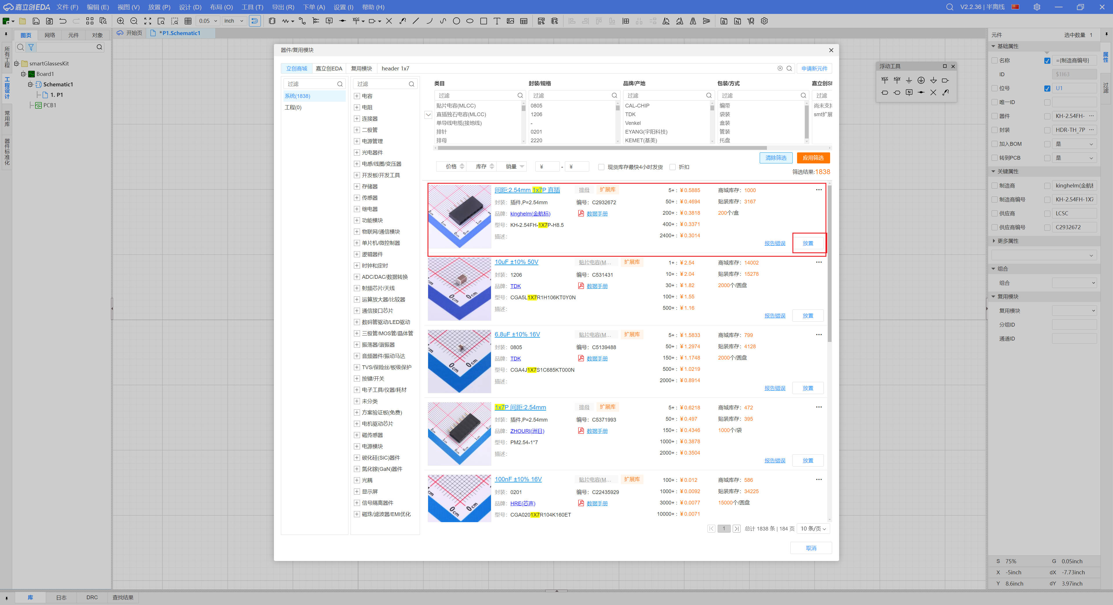
Here is the completed wiring for the module:
1.1.2.3 Display Module
The final module in the schematic was the GAC901 128x128 LCD display.
-
Connector: 12P 0.5mm FPC
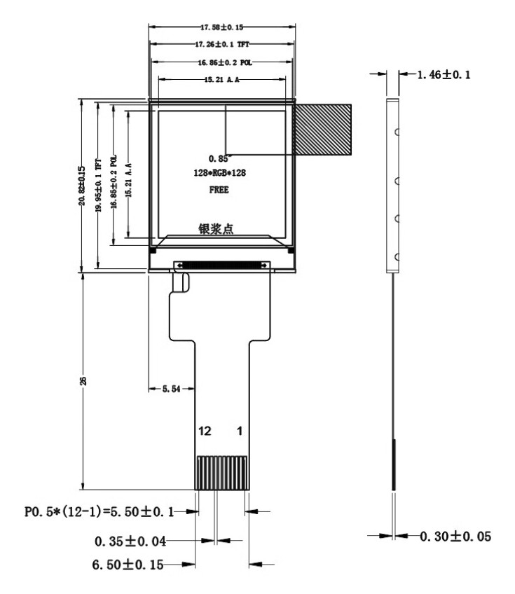
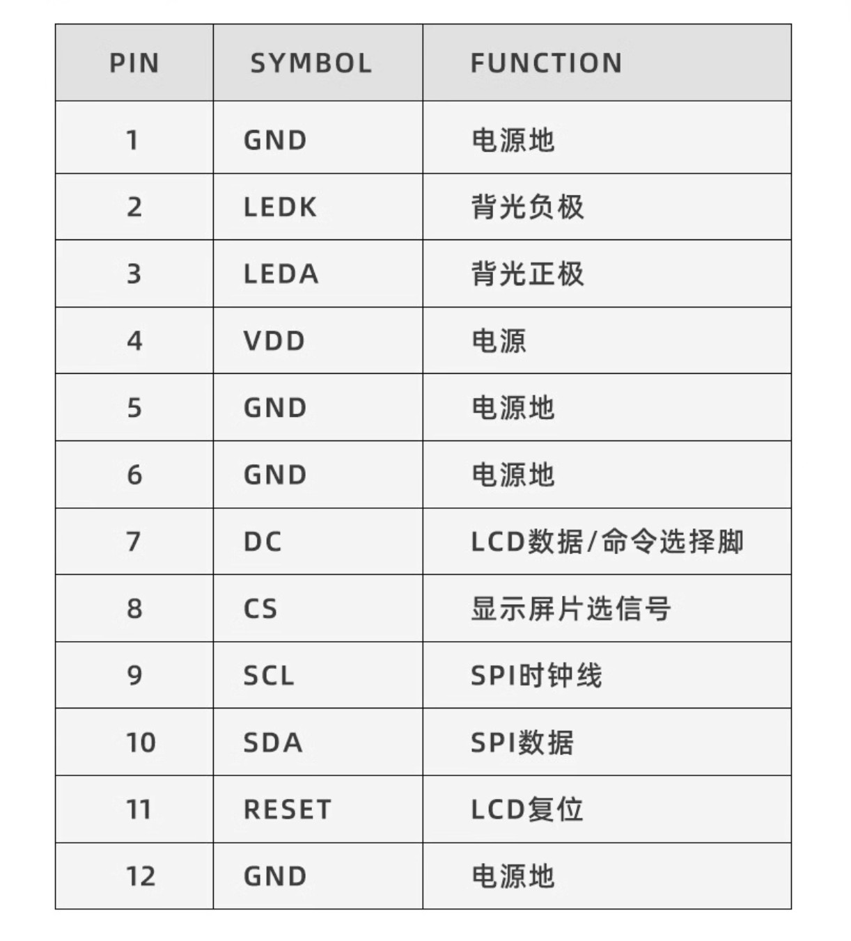
The display wiring was completed as shown below:
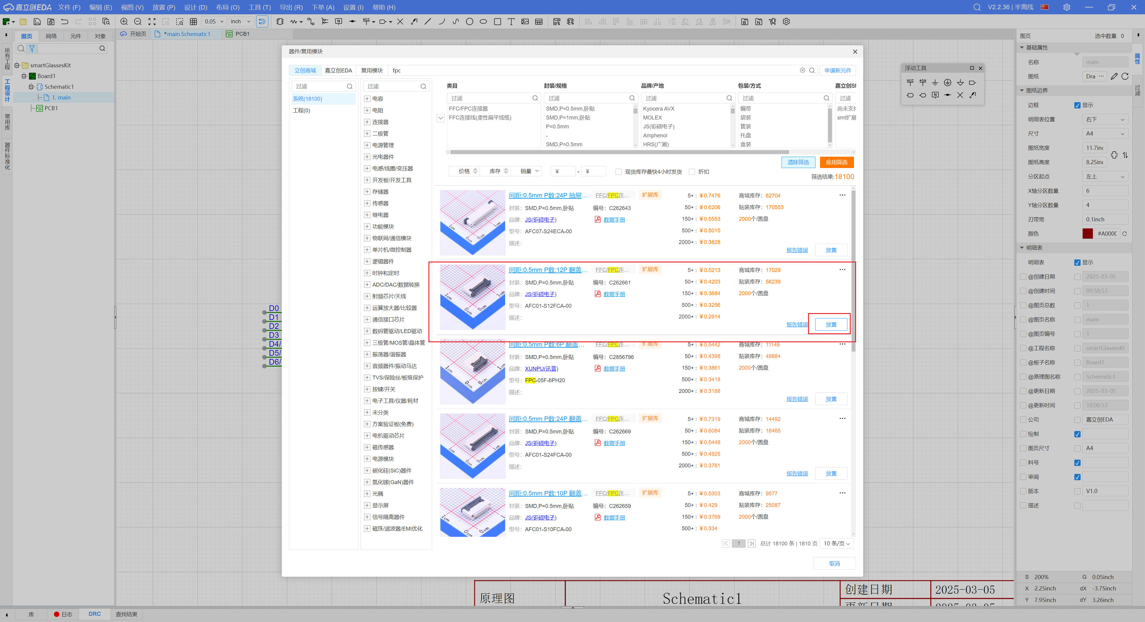
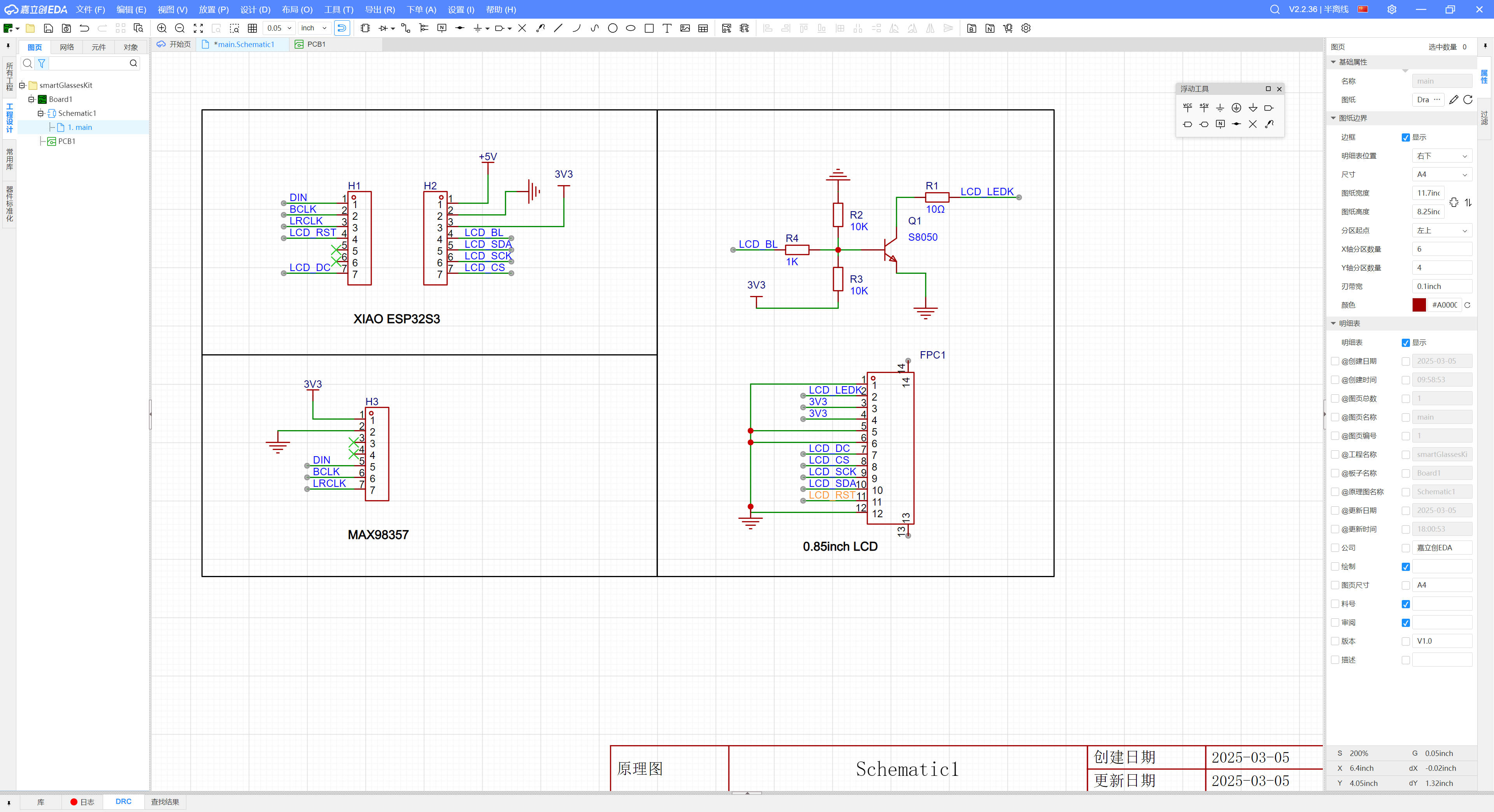
Once all components were added and verified, I moved on to the PCB design.
1.1.3 PCB Design
After completing the schematic, I proceeded to design the PCB layout using 嘉立创EDA.
Synchronization from Schematic
The first step was to synchronize the schematic with the PCB design:
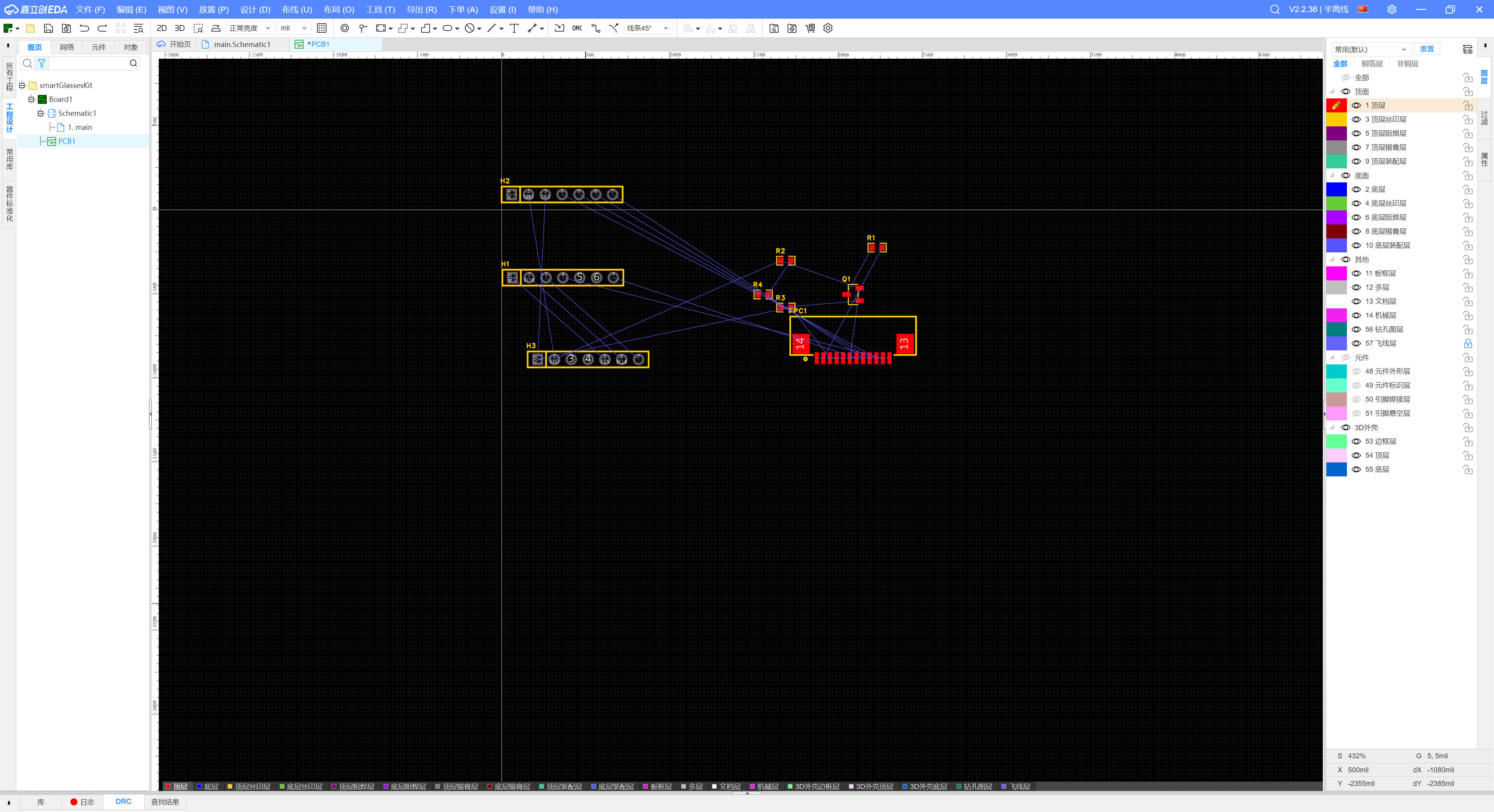
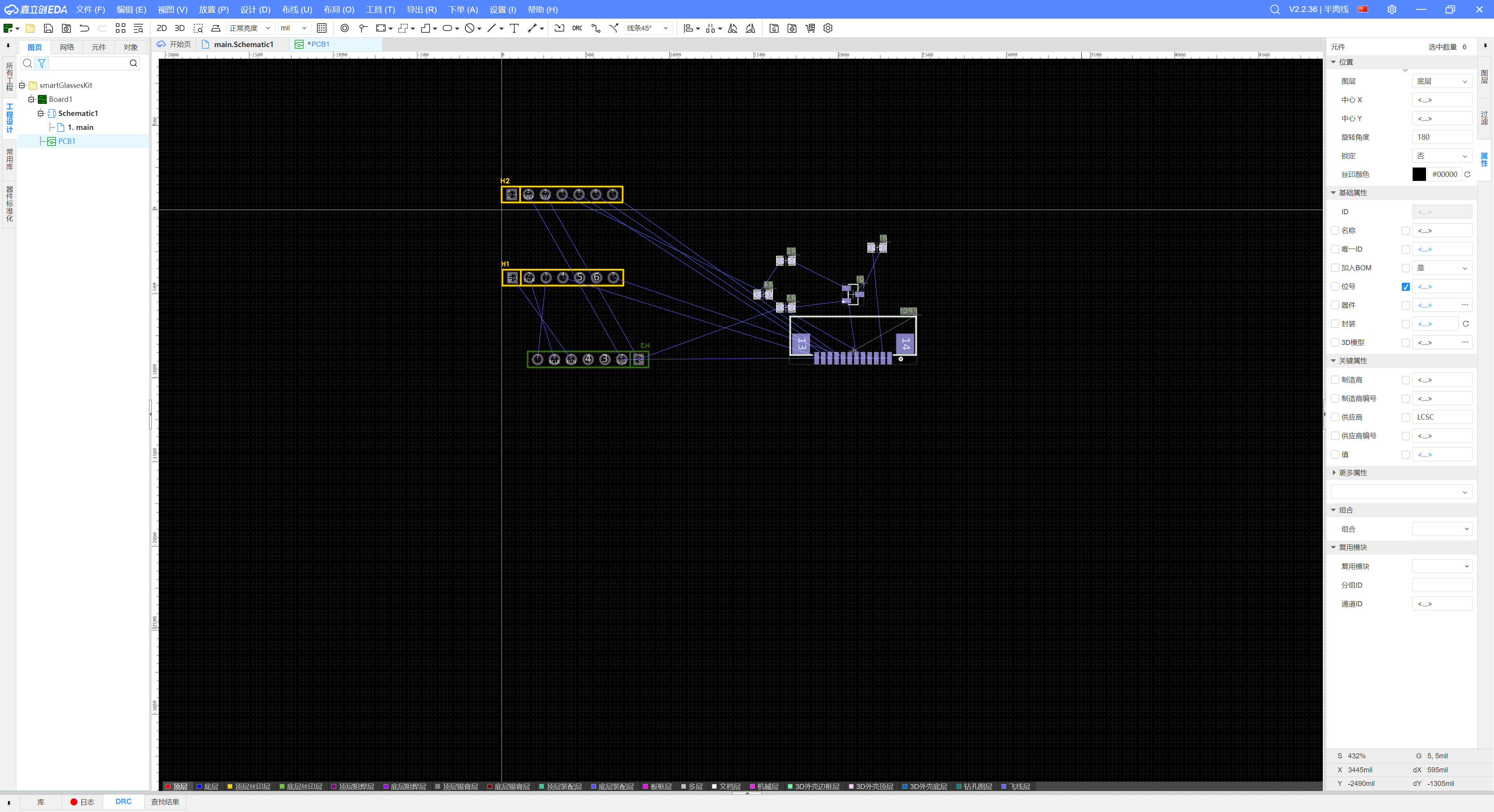
Component Placement
To optimize space, I placed the LCD FPC connector and MAX98357A module on the backside of the PCB:
Routing and Layout
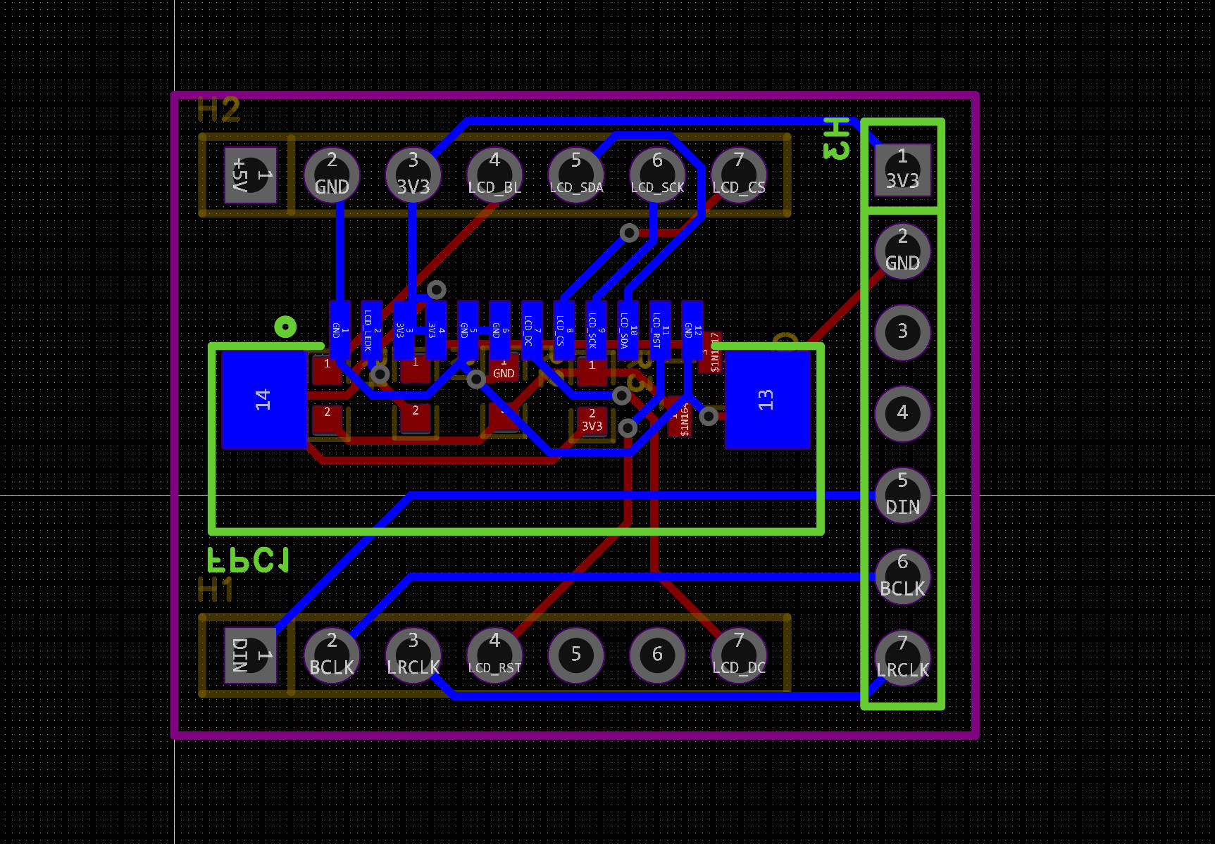
After placing all components, I worked on optimizing the PCB layout to minimize noise and ensure proper signal integrity:
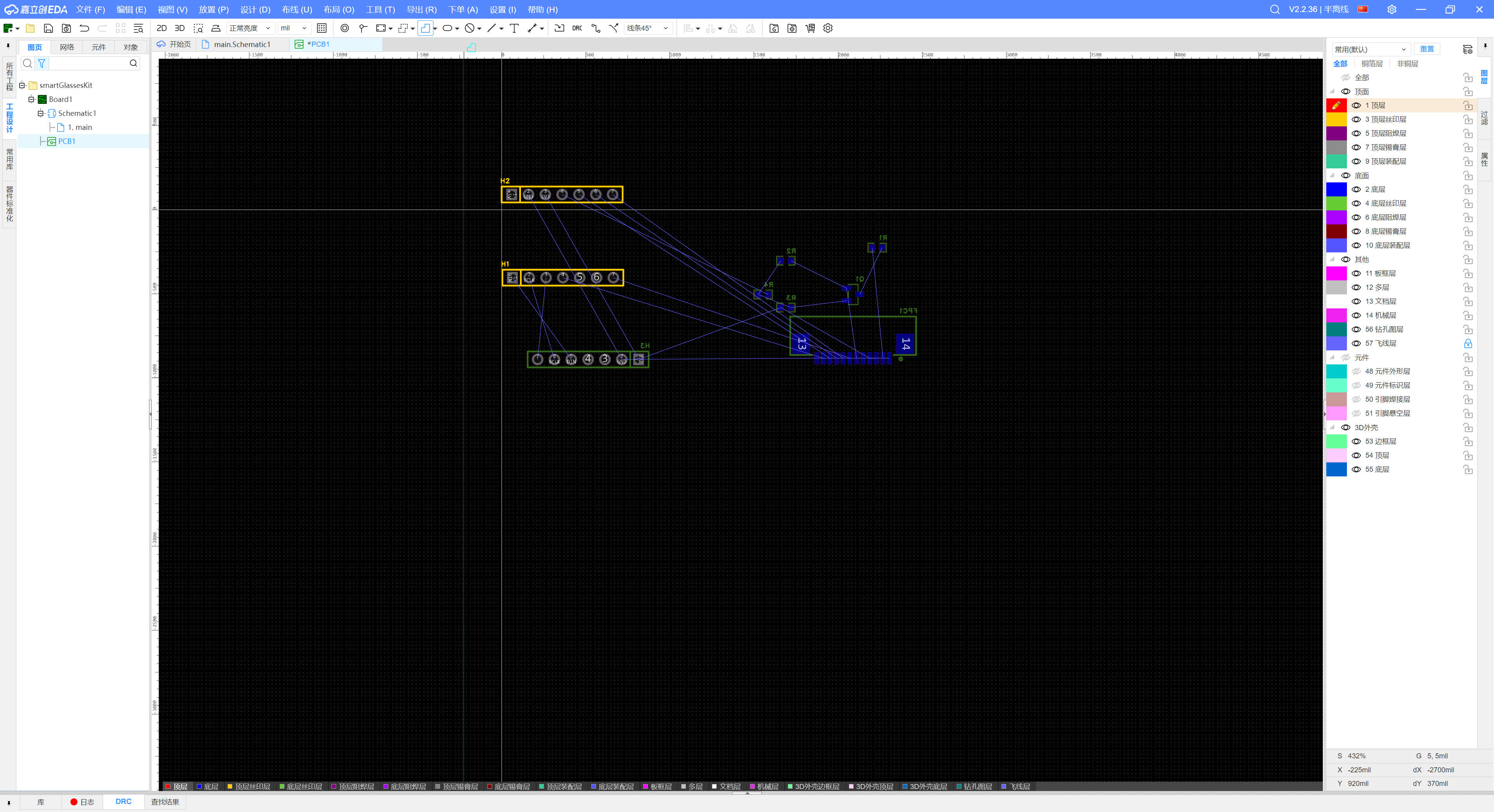
Final PCB layout with routing:
1.1.4 3D Preview
After completing the PCB design, I used 嘉立创EDA to generate a 3D preview of the board to verify component placement and overall design aesthetics:
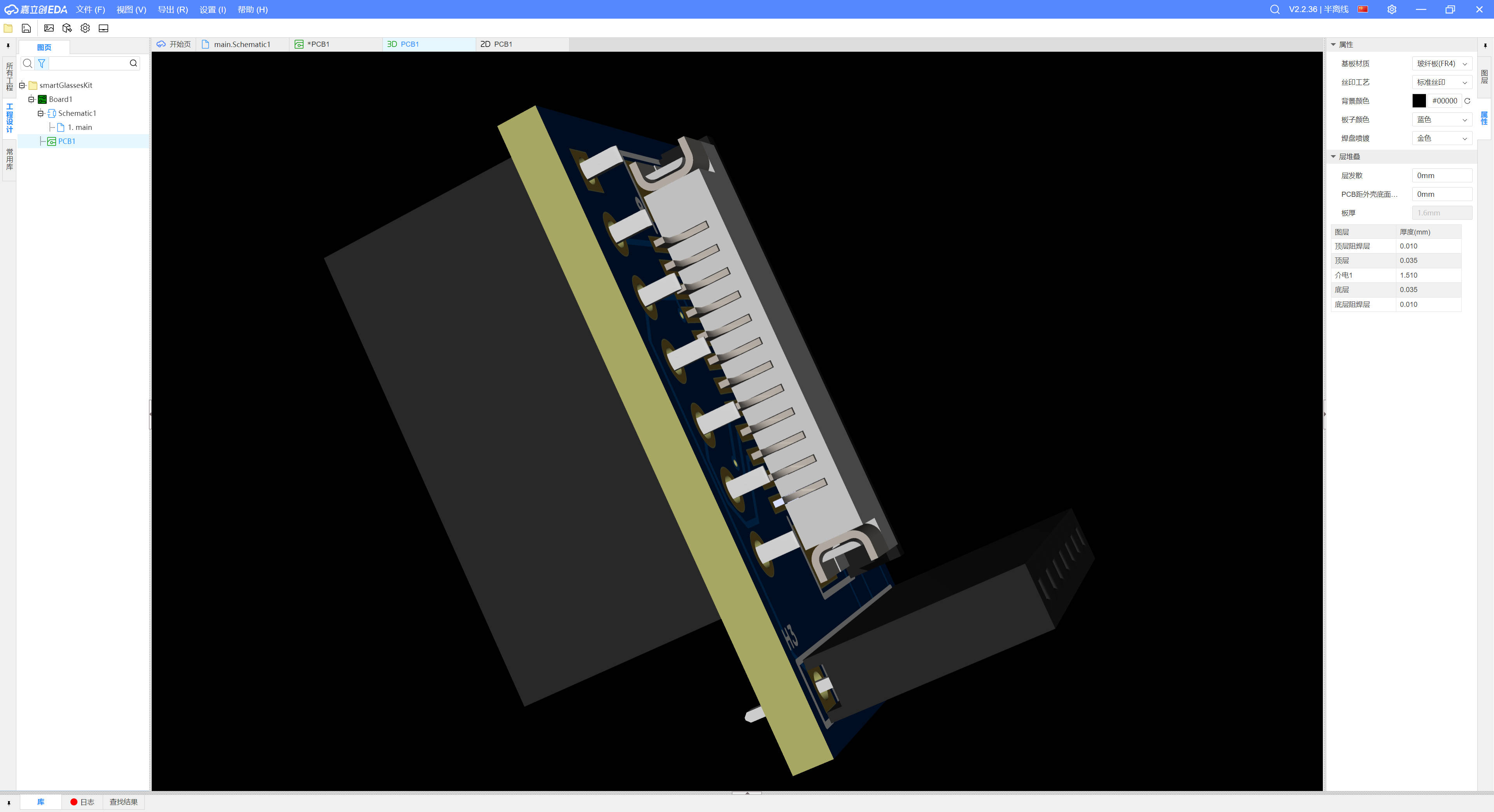
This 3D visualization helped in confirming the design before proceeding with fabrication.
Summary
This week, I successfully designed the electronics hardware for the Smart Glasses Kit, covering:
- Component selection
- Schematic design
- PCB layout
- 3D visualization
With the PCB design finalized, the next step will be prototyping and testing to ensure proper functionality. 🚀