8. Electronics Design
Welcome, this week we will delve into the fascinating world of electronics design, exploring concepts, techniques, and tools essential for designing and prototyping electronic circuits. From understanding basic electronic components to utilizing advanced test equipment, we will embark on a journey to enhance our skills and knowledge in electronics design.
Learning Outcomes:
- Select and use software for circuit board design
- Demonstrate workflows used in circuit board design
Group Assignment:
The group assignment for this week focused on utilizing test equipment in our lab to observe the operation of a microcontroller circuit board. The main tasks included demonstrating the use of a multimeter and an oscilloscope, as well as sending a PCB out to a board house. We documented our work on the group page
Multimeter Exploration
We began by delving into the functionality and features of a multimeter. This versatile tool allowed us to measure various electrical parameters such as voltage, current, resistance, and continuity. We conducted a continuity test on a PCB to ensure all tracks were properly connected. The multimeter served as a reliable tool to identify any potential faults or discontinuities in the circuitry, providing valuable insights into the integrity of the PCB’s connections.
Voltage Measurement
Moving on, we focused on measuring the voltage levels at different points of the microcontroller board, including the 5V and 3.3V pins. This enabled us to verify the proper functioning of the power supply circuitry and ensure that the microcontroller received the required voltage levels for operation. Additionally, we performed voltage measurements on an analog sensor, utilizing both the multimeter and the oscilloscope. This comparative analysis allowed us to evaluate the effectiveness of each tool for sensor measurement tasks and understand the advantages offered by the oscilloscope in capturing dynamic voltage variations with greater precision.
Oscilloscope Analysis
Exploring the features and settings of the oscilloscope was an enlightening experience. We used the oscilloscope to visualize the voltage output of the analog sensor, gaining valuable insights into the behavior of the sensor and its voltage variations over time. The oscilloscope’s ability to display waveform traces in real-time provided a comprehensive understanding of the sensor’s response to external stimuli, enhancing our knowledge of signal analysis and interpretation.
LED Testing
Finally, we programmed the microcontroller board to perform blink and PWM (Pulse Width Modulation) tests on an LED. This practical experiment allowed us to observe the voltage level changes during these tests using the oscilloscope. By analyzing the waveform shape and dynamics, we gained a detailed understanding of the LED’s behavior under different operating conditions, further solidifying our grasp of electronics design principles.
Overall, the group assignment provided us with valuable hands-on experience in utilizing test equipment and conducting various electronic measurements. It enhanced our understanding of electronics design concepts and equipped us with essential skills for prototyping and troubleshooting electronic circuits.
Individual Assignment: Designing a Development Board
Introduction
In this individual assignment, I embarked on the journey of electronics design, starting with setting up KiCad and progressing through schematic design, PCB layout, fabrication, and testing. This documentation outlines the step-by-step process I followed to create and prototype a custom PCB.
Setting Up KiCad
I began by downloading and installing KiCad, an open-source electronics design automation suite. Additionally, I installed the Fab library to access a wide range of component footprints required for my project.


Creating the Project
- Starting a New Project: Within KiCad, I initiated a new project to begin the design process.
- Schematic Editor: I entered the schematic editor to conceptualize and layout the circuit components.
Schematic Design
- Inserting Components: Using the component library, I inserted all necessary components onto the schematic.

Component Selection and Rationale:
In designing my custom PCB, I carefully selected each component to ensure the board’s functionality and future expandability:
- XIAO-RP2040: Chosen for its powerful microcontroller capabilities, providing a robust foundation for the development board.
- LED_1206: Utilized for testing and indication purposes, offering a clear visual signal for debugging and functionality checks.
- Conn_01x04_Pin: This connector facilitates I2C connections, allowing for easy integration of additional components and future expansion.
- Conn_PinHeader_1x07_P2.54mm_Vertical_THT_D1mm: Two of these headers were included to connect all the pins of the XIAO, enabling the addition of various components and peripherals in the future.
- Switch_Tactile_Omron: This tactile switch is used for controlling different features and is particularly useful during programming and testing of the development board.
- Buzzer: Added as an output device, the buzzer will be employed in future applications and programming to provide auditory feedback.
-
Resistors: Various resistors were incorporated to support the LED and button functionalities, ensuring proper operation and acting as pull-up resistors where necessary.
-
Assigning Footprints: Each component was assigned the appropriate footprint to ensure compatibility with the PCB layout.
-
Connecting Components: I established connections between components to form the desired circuitry.

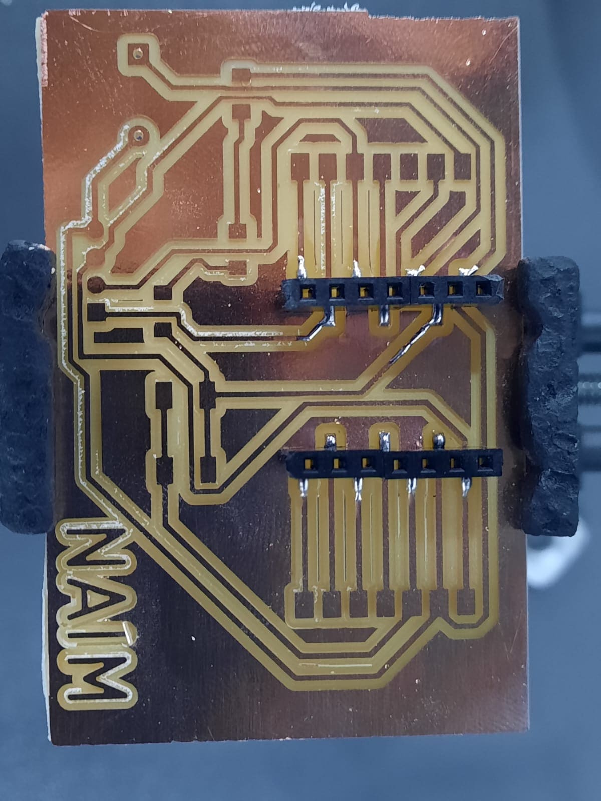
PCB Layout
-
Transitioning to PCB Editor: After completing the schematic design, I moved to the PCB editor to translate the schematic into a physical layout.
-
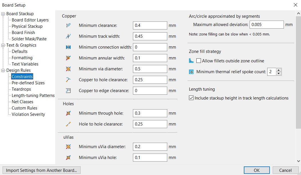
Defining Board Constraints
I defined specific constraints for the PCB layout to ensure manufacturability and functionality:
-
Minimum Distance Between Tracks: Set at least 0.4mm to prevent signal interference.
-
Minimum Track Width: Tracks were designed to be at least 0.45mm wide to handle current requirements adequately.
-
Importing Components and Connections: Components and their connections were imported from the schematic to the PCB layout.
-
Arranging Components: I strategically arranged components on the PCB layout to optimize space utilization and signal integrity.
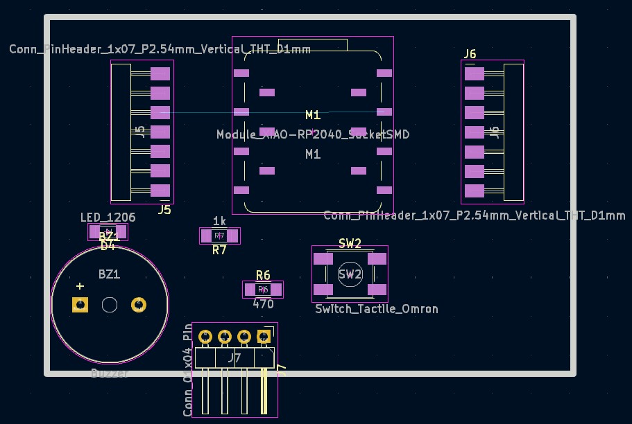
- Connecting Components with Traces: Traces were routed to establish electrical connections between components while adhering to design constraints.

Verification and 3D Visualization
I conducted a thorough verification of the PCB layout to check for errors and completeness. Additionally, I utilized the 3D viewer to visualize component placement and ensure proper clearance.
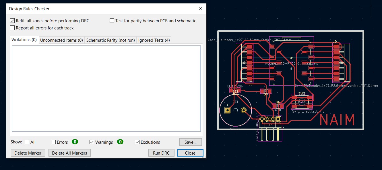
Using the Design Rule Checker (DRC)
To ensure the PCB layout was error-free and met all design constraints, I utilized KiCad’s Design Rule Checker (DRC). After completing the layout, I ran the DRC to verify the design and ensure there were no warnings or errors. This step confirmed that the PCB design was ready for fabrication.
Using the 3D Viewer
To ensure the proper placement of components and to visualize the final look of the PCB, I utilized KiCad’s 3D viewer. After completing the PCB layout, I opened the 3D viewer from within KiCad to inspect the board. I rotated and zoomed in on the board to check for any visual discrepancies or placement issues. Using the 3D viewer, I confirmed that all components were correctly placed and that there were no clearance issues, ensuring that the PCB was ready for fabrication.

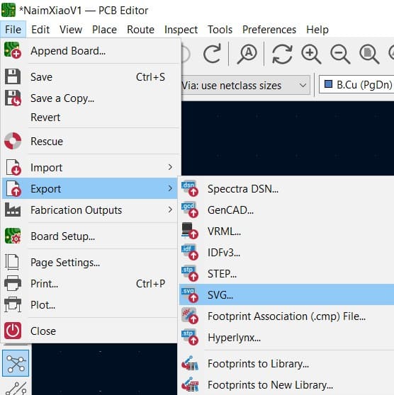
Exporting PCB Files
- Exporting SVG Files: I exported SVG files for traces, drills, and outline from KiCad, which are essential for further processing.

Editing SVG Files
I utilized Inkscape to make any necessary modifications to the exported SVG files, ensuring alignment with fabrication requirements.
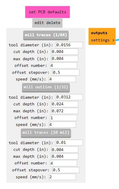
Creating Toolpaths

- Importing SVG Files: Modified SVG files were imported into Mods software, a PCB milling tool.

- Generating Toolpaths: I generated toolpaths in Mods software to facilitate the PCB milling process accurately.
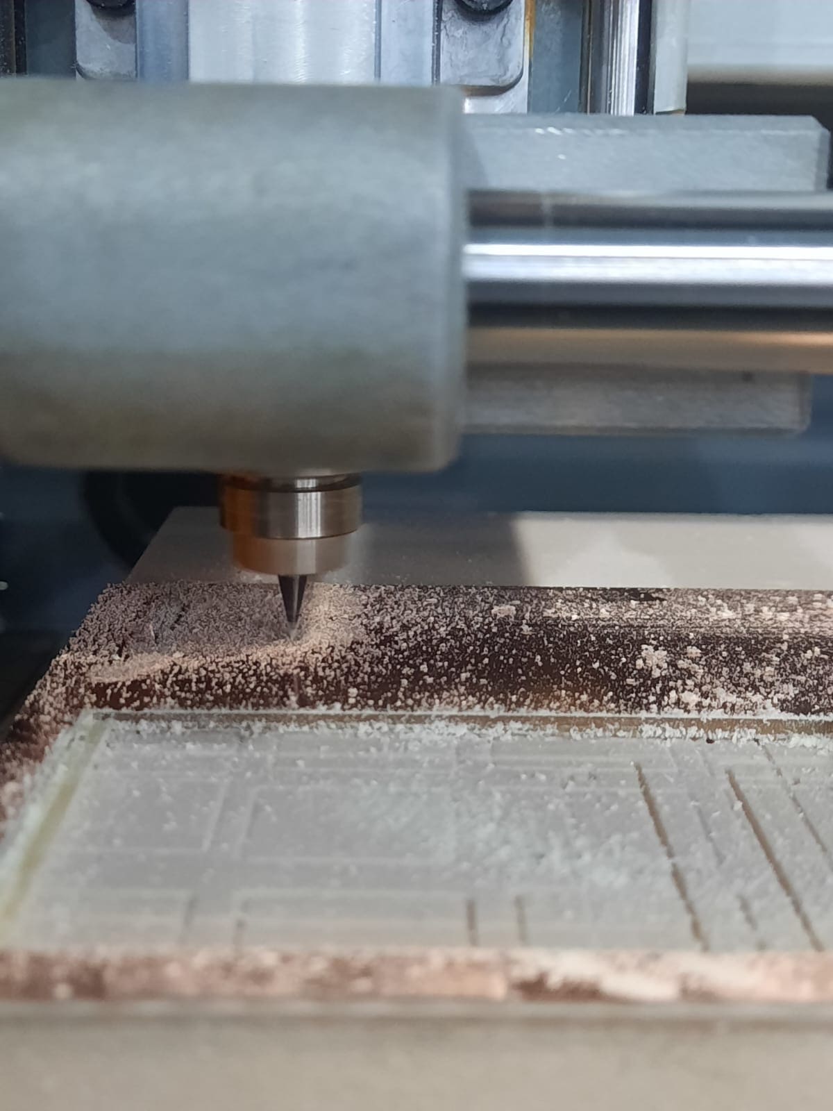
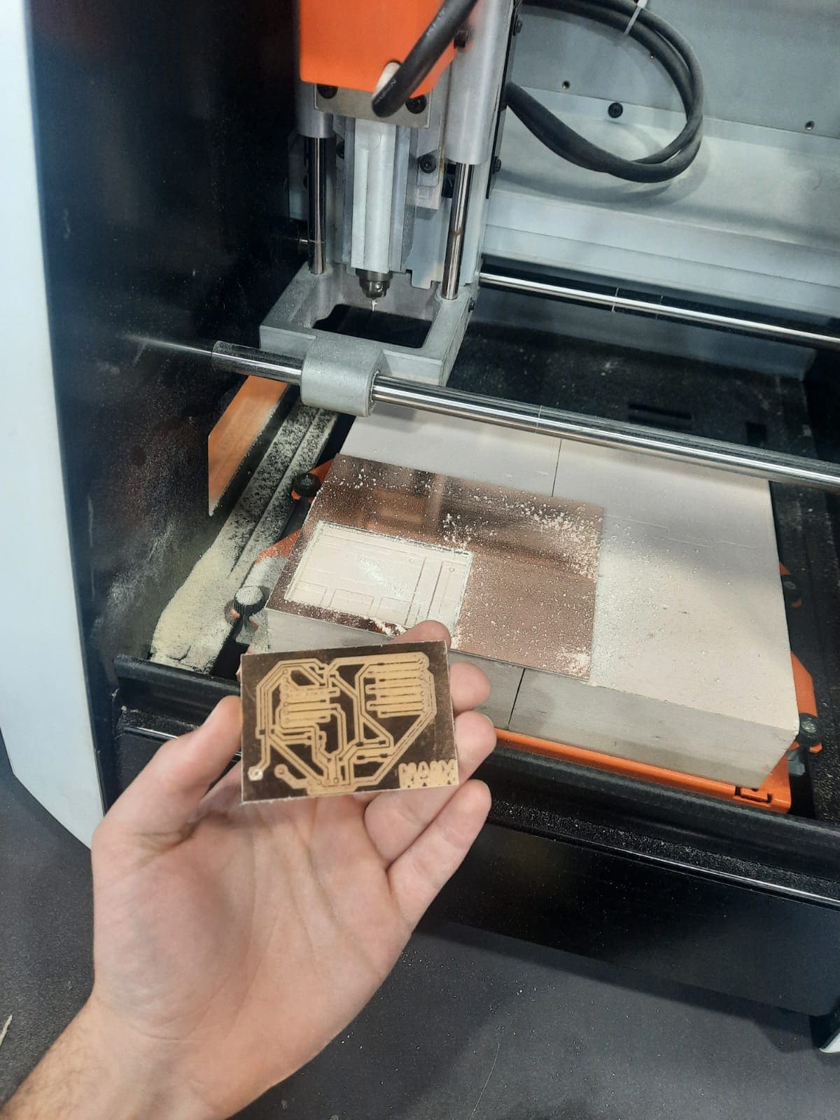
PCB Fabrication
I proceeded to mill the PCB using the generated toolpaths, ensuring precise fabrication according to design specifications.

Assembly and Testing
- Soldering Components: Components were soldered onto the fabricated PCB with attention to detail and accuracy.


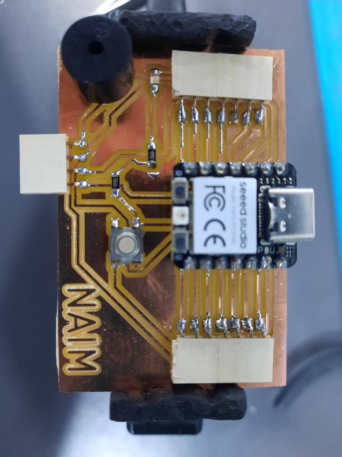
- Testing Functionality: The functionality of the completed PCB was tested to validate its performance and reliability.
Conclusion
Through this individual assignment, I gained valuable hands-on experience in electronics design, from conceptualization to prototyping. The process of creating a custom PCB equipped me with practical skills and insights essential for future electronics projects.