In week 4, I learned how to make a PCB (Printed Circuit Board) called Quentorres. It was my first time doing an activity like this, so it was especially challenging to understand and learn the names of all the small components and distinguish them from each other. Additionally, it was my first time using a milling machine and soldering, which was quite a task! Finally, I successfully programmed the board. It was truly a week of intensive learning.
Characterize the design rules for your in-house PCB production process: document feeds, speeds, plunge rate, depth of cut (traces and outline) and tooling.
Document the workflow for sending a PCB to a board house.
Document your work to the group work page and reflect on your individual page what you learned.
Individual assignment:
Make and test a microcontroller development board.
Learning Outcomes
Described the process of tool-path generation, milling, stuffing, de-bugging and programming.
Demonstrate correct workflows and identify areas for improvement if required.
Results: Electronics Production
After performing all the tasks that I will describe in the content of this page, I managed to manufacture the Quentorres PCB.
Quentorres PCB
And I manage to make it work with this code in Arduino IDE!
const int ledPin = D7; // Pin D7 on Xiao rp2040

// the setup function runs once when you press reset or power the board
void setup() {
  // initialize digital pin LED_BUILTIN as an output.
  pinMode(ledPin, OUTPUT);
}

// the loop function runs over and over again forever
void loop() {
  digitalWrite(ledPin, HIGH);       // turn the LED on (HIGH is the voltage level)
  delay(1000);                      // wait for a second
  digitalWrite(ledPin, LOW);        // turn the LED off by making the voltage LOW
  delay(1000);                      // wait for a second
}
Quentorres PCB code in Arduino IDE for blinking program
Preliminary Concepts
Since I am almost completely new to this topic, I have documented everything I learned this week. Even what may seem super basic to those who know the subject. Thanks to my tutors and their teachings I understood most of the terms this week. I think I will end up understanding and assimilating the rest in the following weeks as we work on electronic topics.
Printed Circuit Board
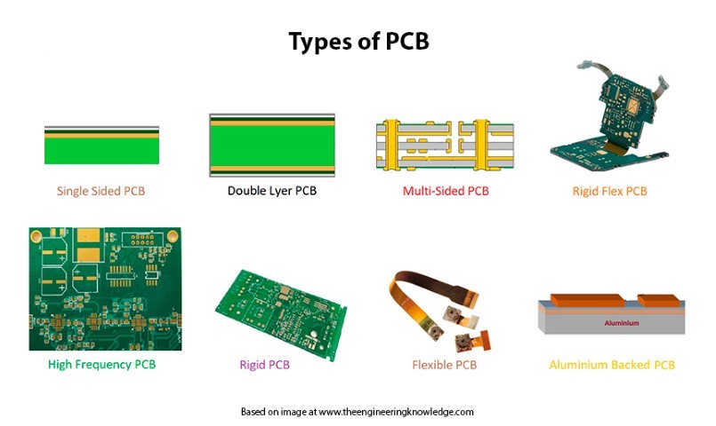
A Printed Circuit Board or PCB is a mechanical support that allows electronic components to be electrically interconnected. It emerged as a solution to a problem in the old (and messy by current standards) manufacturing of electronic boards. These are classified by their rigidity and number of layers.
PCB types
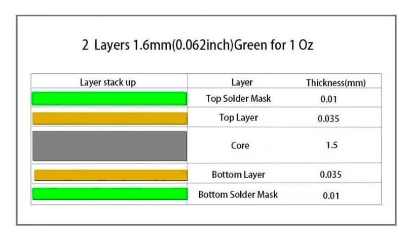
PCBs are made up of two layers of copper at the top and bottom, while in the middle they have a carrier material.
To test the parameters of the milling machine, I went to the Universidad Cientifica del Sur (UCSUR) Fab Lab which is located in the architecture faculty of the university, in Chorrillos district, in the city of Lima, Peru.
The machine used was the Roland monoFab SRM-20. It is a compact 3D milling machine used for prototyping in chemical wood, acrylic and modeling wax with a milling area of 200mm x 150mm x 60mm. It usually includes the MODELA Player 4, iMODELA Creator and ClickMILL softwares. Additionally, it uses VPanel for operating it. To mill the initial tests and the board, I used iMODELA Creator to configure the traces and VPanel to operate the machine.
Roland monoFab SRM-20 and mills
Image transfer
There are several ways to transfer the copper path on the PCB: photographic method, silkscreen method, thermal transfer method, CNC milling method, among others. In this case, I worked with the latest method to manufacture my PCB.
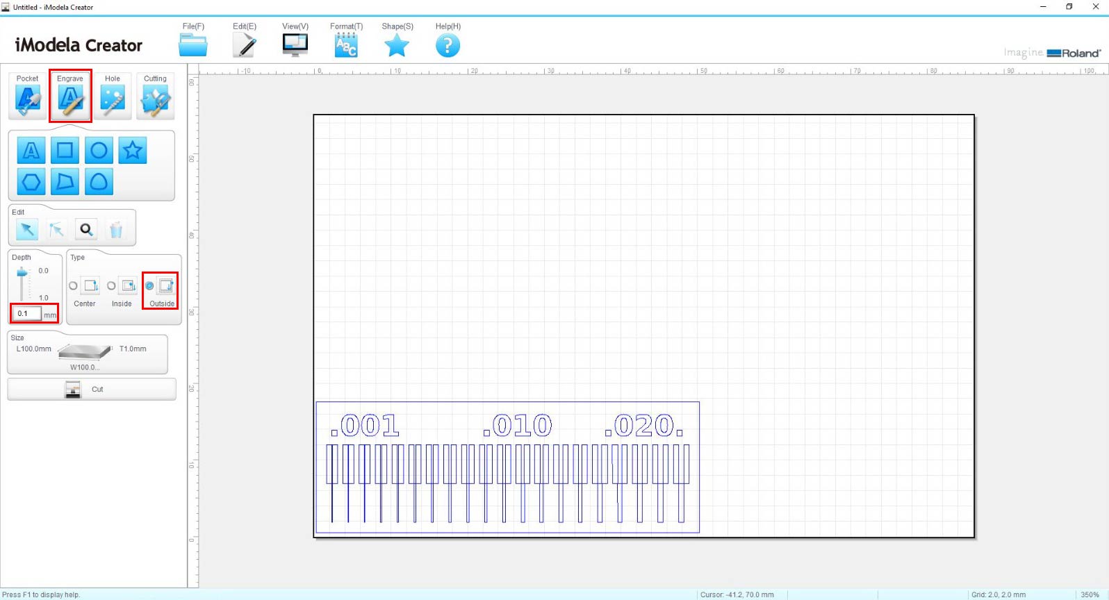
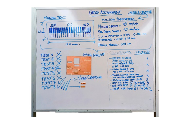
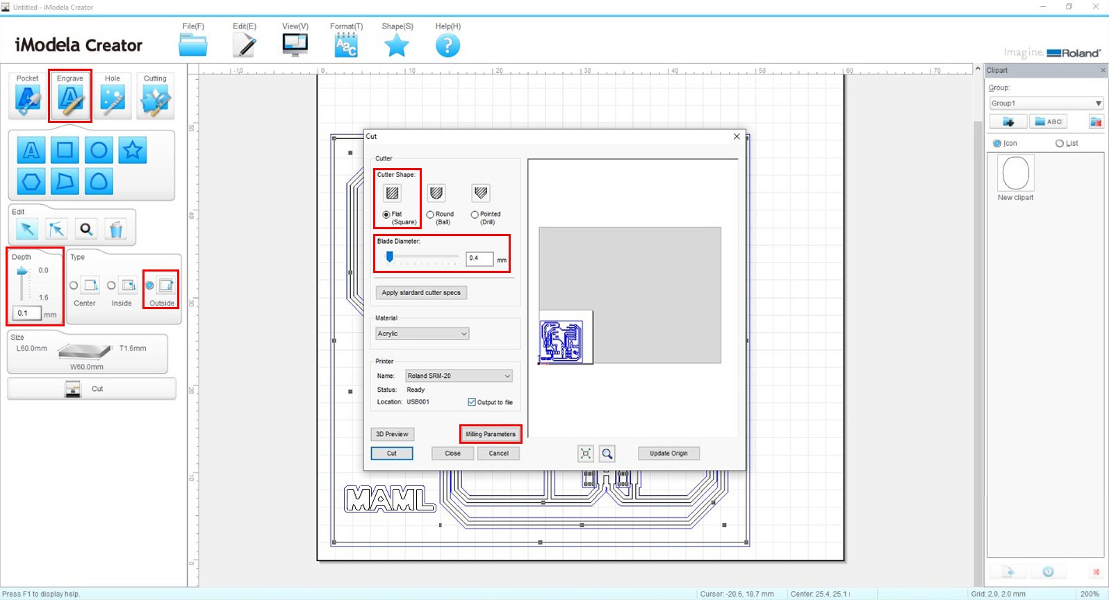
As a group, we tested the milling precision with this traces test. First, we downloaded the file, opened iModela Creator and imported the design file. Then, we configured the parameters. This was a trial and error process in which it took us seven tests to arrive at the ideal parameters. Mode: Engrave | Depth: 0.1mm | Type: Outside | Cutter shape: Flat | Blade diameter: 0.4 mm | Milling speed: 90/90 mm/min | Tool down speed: 90/90 mm/min | Cut-in amount: 0.04/0.2 mm | Stepover: 0.20/ 0.10 mm | Finish margin: 0.01 mm.
Configuring correct test parameters in iModela Creator
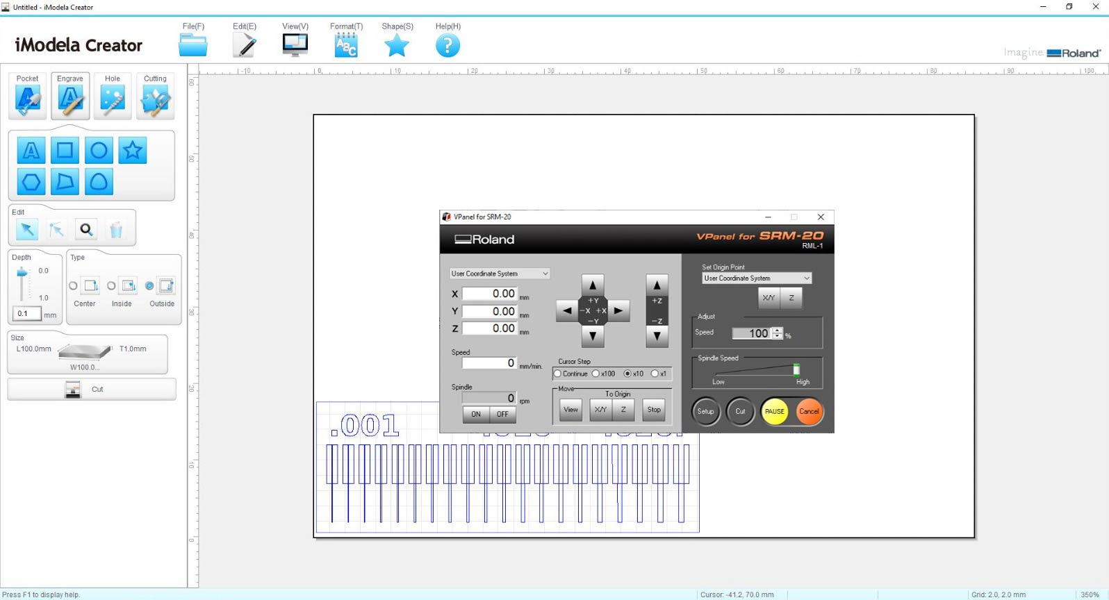
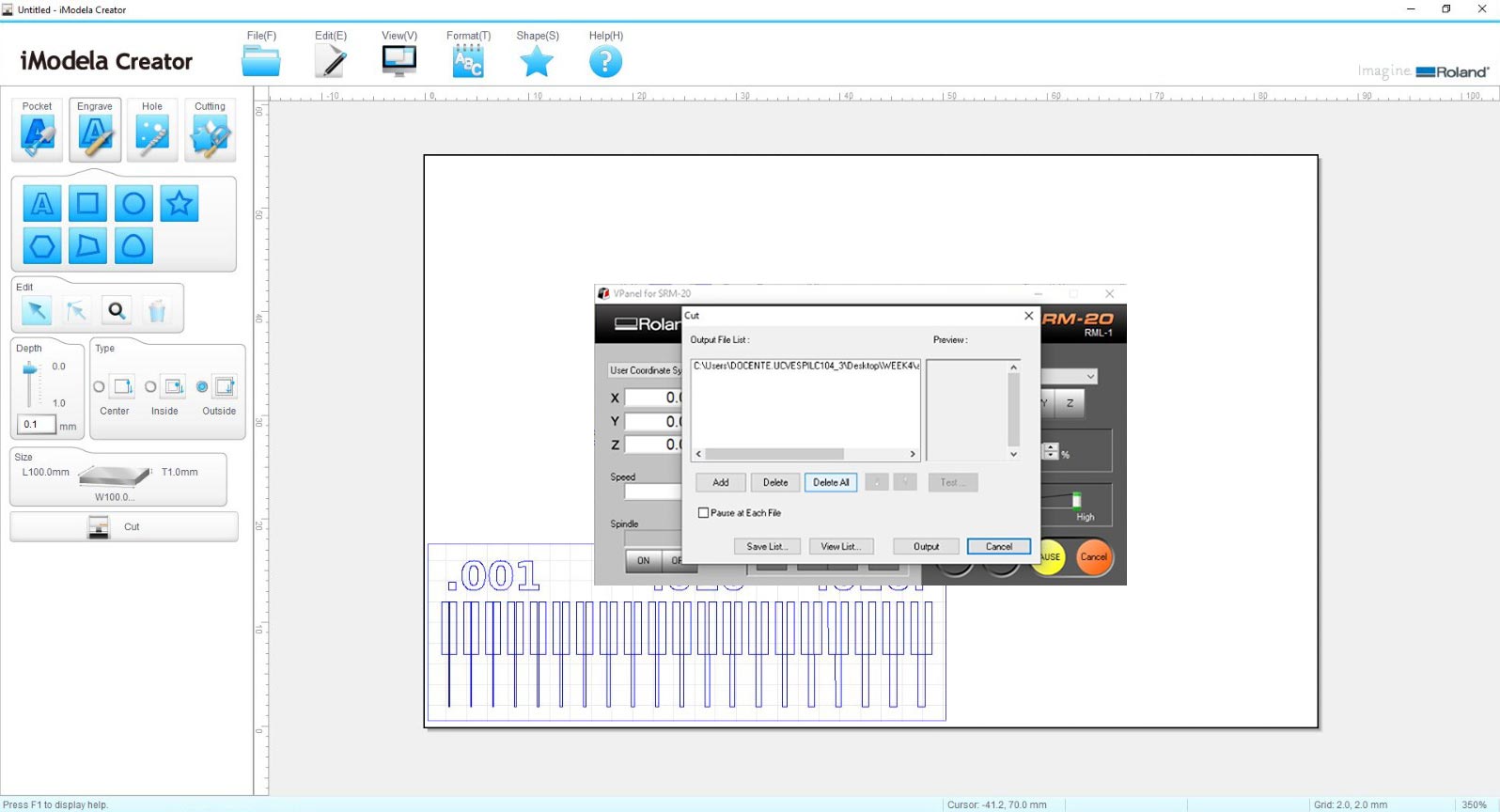
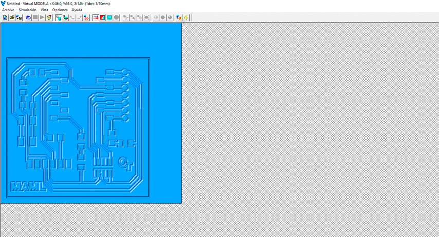
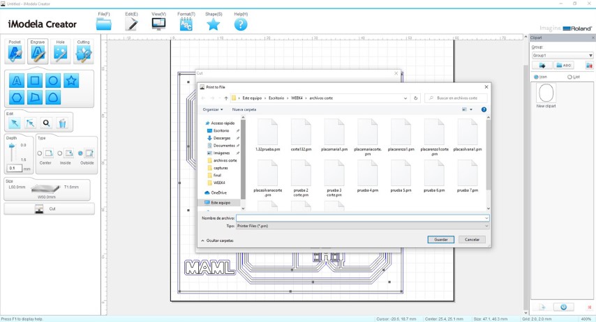
Once the test file was set up, the milling cutter had to be calibrated with the paper method before the test file was manufactured. Then, we secured the copper board to the machine bed using double-sided tape. With the machine and board ready, we opened Vpanel, set the origin point for the milling job, loaded and saved the tool path of the design (previously generated in iModela Creator). Finally, we started the milling process.
Vpanel configurations
Calibrating the machine with the paper method for milling the test and milling parameters in iMODELA Creator
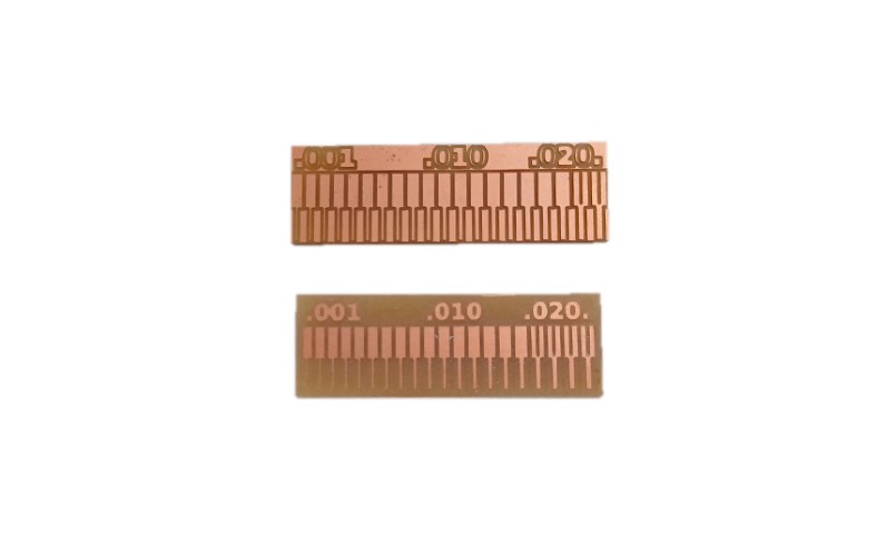
Finally, this was the result (after many attempts).
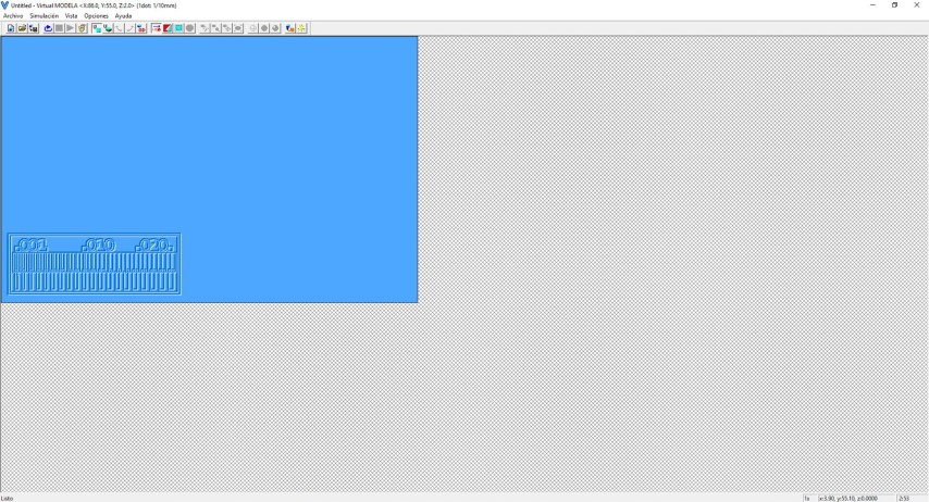
Sixth and seventh milling test
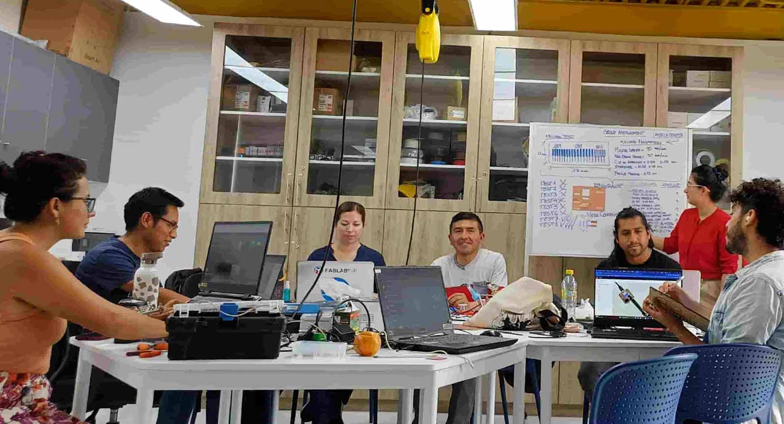
Working as a team this week was essential for me because I was able to learn from colleagues who had more experience in the subject.
Work team at Fab Lab
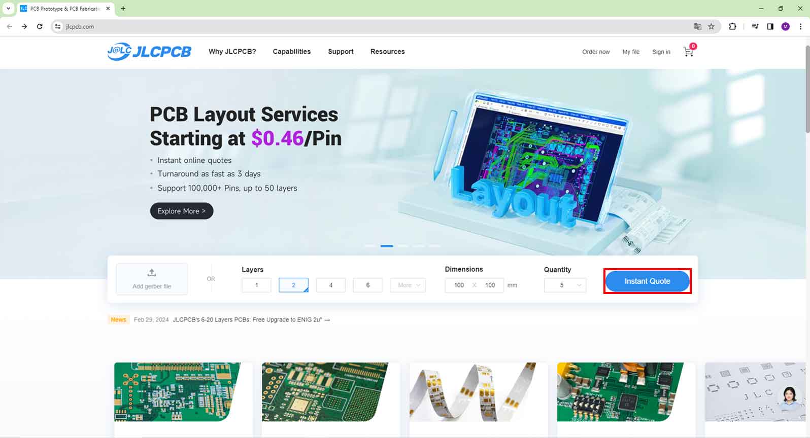
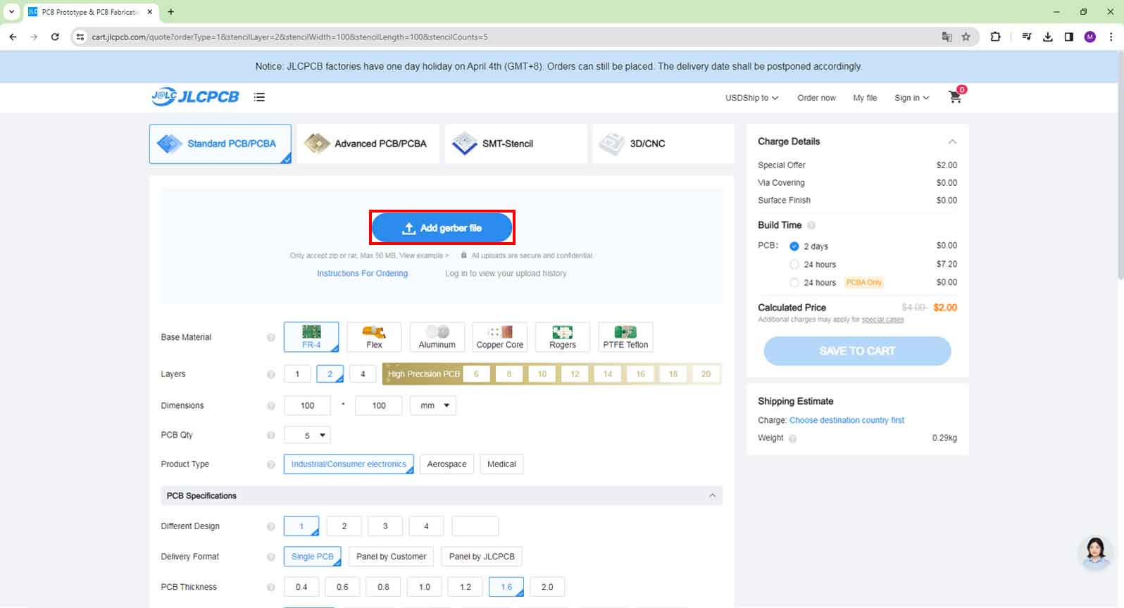
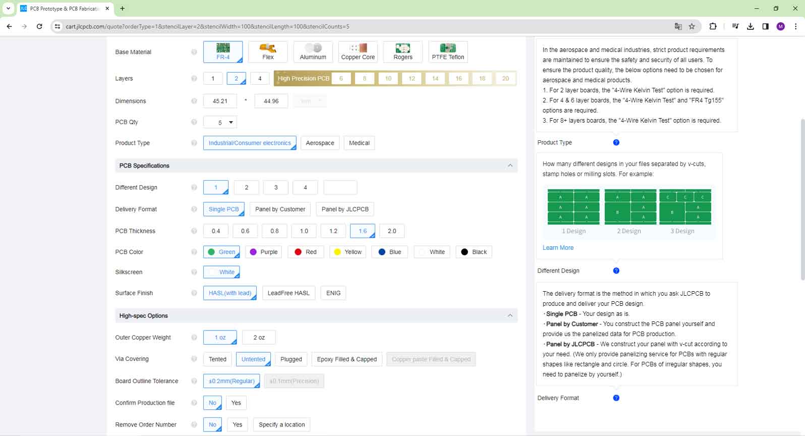
Sending Quentorres to a Board House
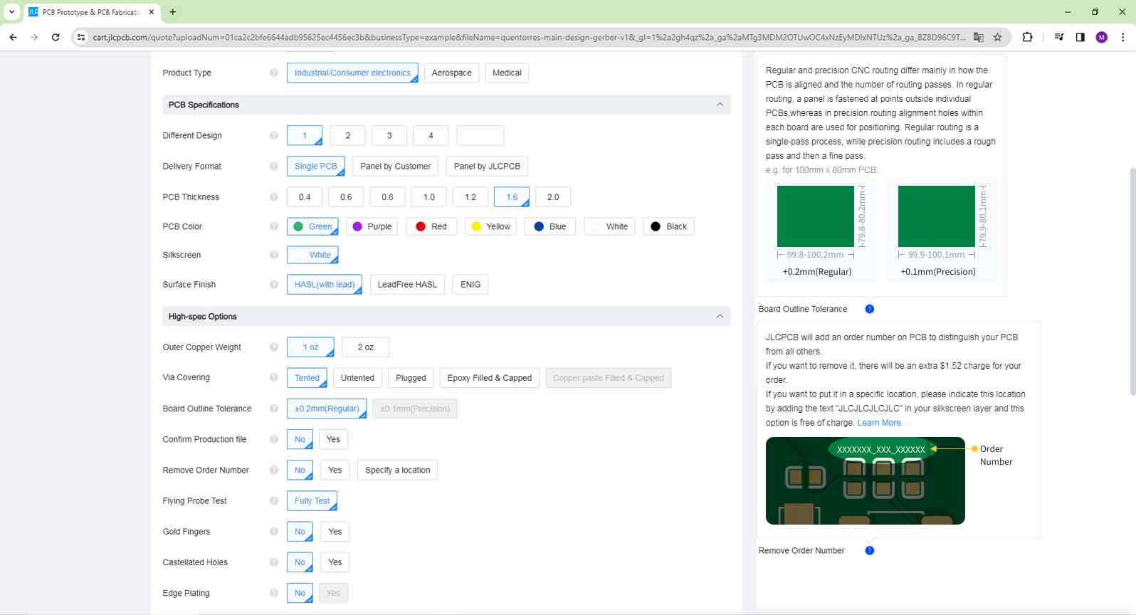
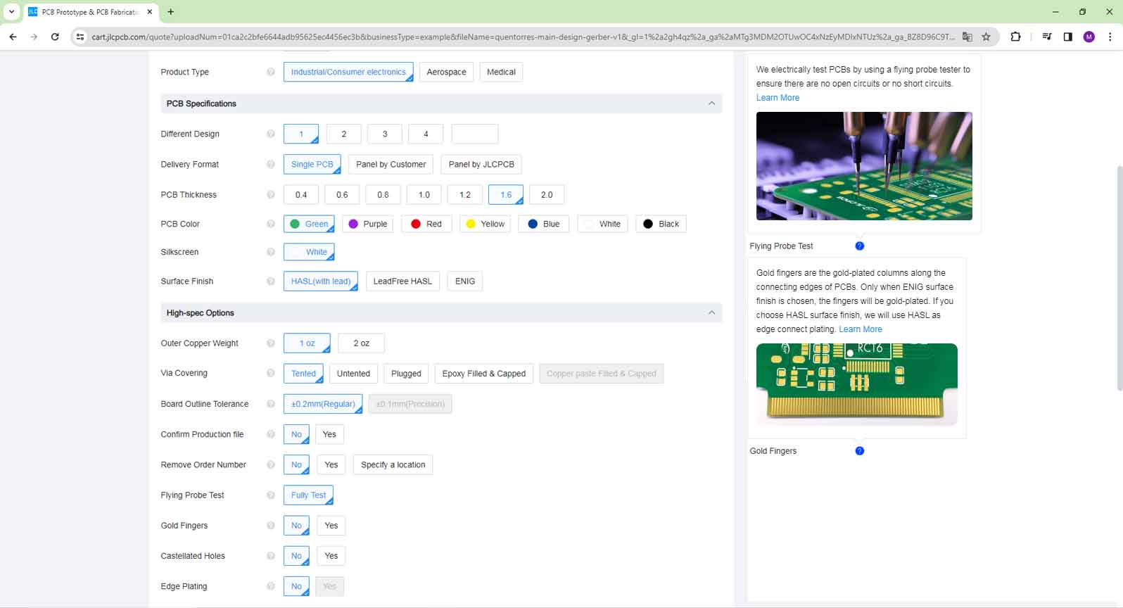
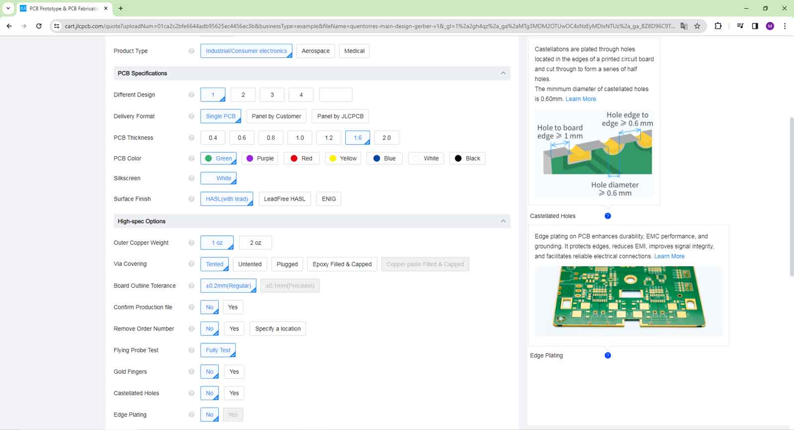
Founded in 2006, JLC works on building a one-stop industrial electronic platform, realizing digital PCBA processing by incorporating EDA, PCB, parts sourcing, and PCBA services. For the assignment of this week, I sent the Quentorres PCB to this board house.
Proccess of sending Quentorres to JLCPCB
With those characteristics, the board costs $2.00 and weight 0.15kg in JLCPCB.
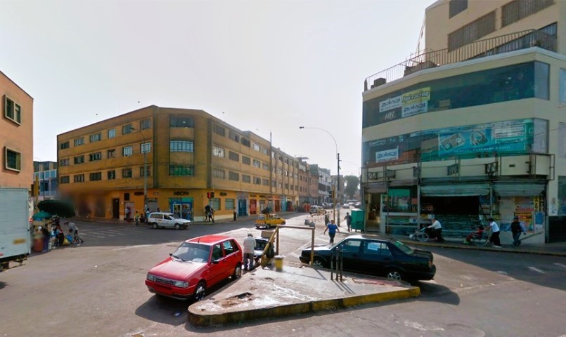
Paruro Market: Getting the Electronic Components
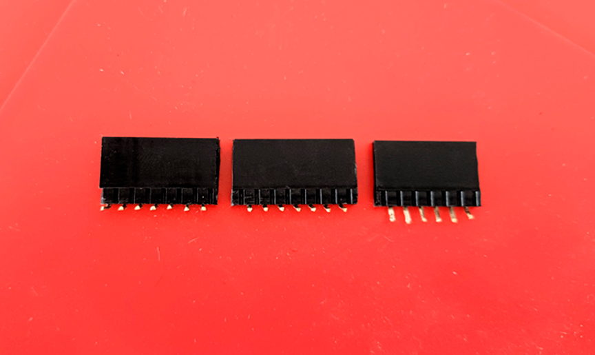
For getting the necessary materials for completing this assignment, I needed to import the Xiao RP2040 -with the support of my tutors- and purchased the rest of the components. In Peru SMD components are very scarce, so as a group, Fab Lab Lima students helped each other for obtaining the components we needed. We went shopping in Paruro, the mecca of electronic components in the country and modified some of the components we got. The stores where we got the components were: Electron (located in 1357 Paruro Street), TEZLA - Electrónica Industrial Store (located in 1329-1349 Paruro Street, store 36), and Boy Jaramillo Segundeo Pablo Store (located in 1353 Paruro Street, store 239).
Paruro street market
Purchased components in Paruro
Now with the necessary supplies, we returned to the fab lab to manufacture the PCBs.
Individual Assignment: Quentorres PCB
The Quentorres PCB is the combination of a programmer to rule them all and a hello board to learn to program. The original programmer created by Quentin Bolsée and redesigned by Adrián Torres. Quentorres is born at the 2024 Instructors Bootcamp held in León. Logo made by Miriam Choi.
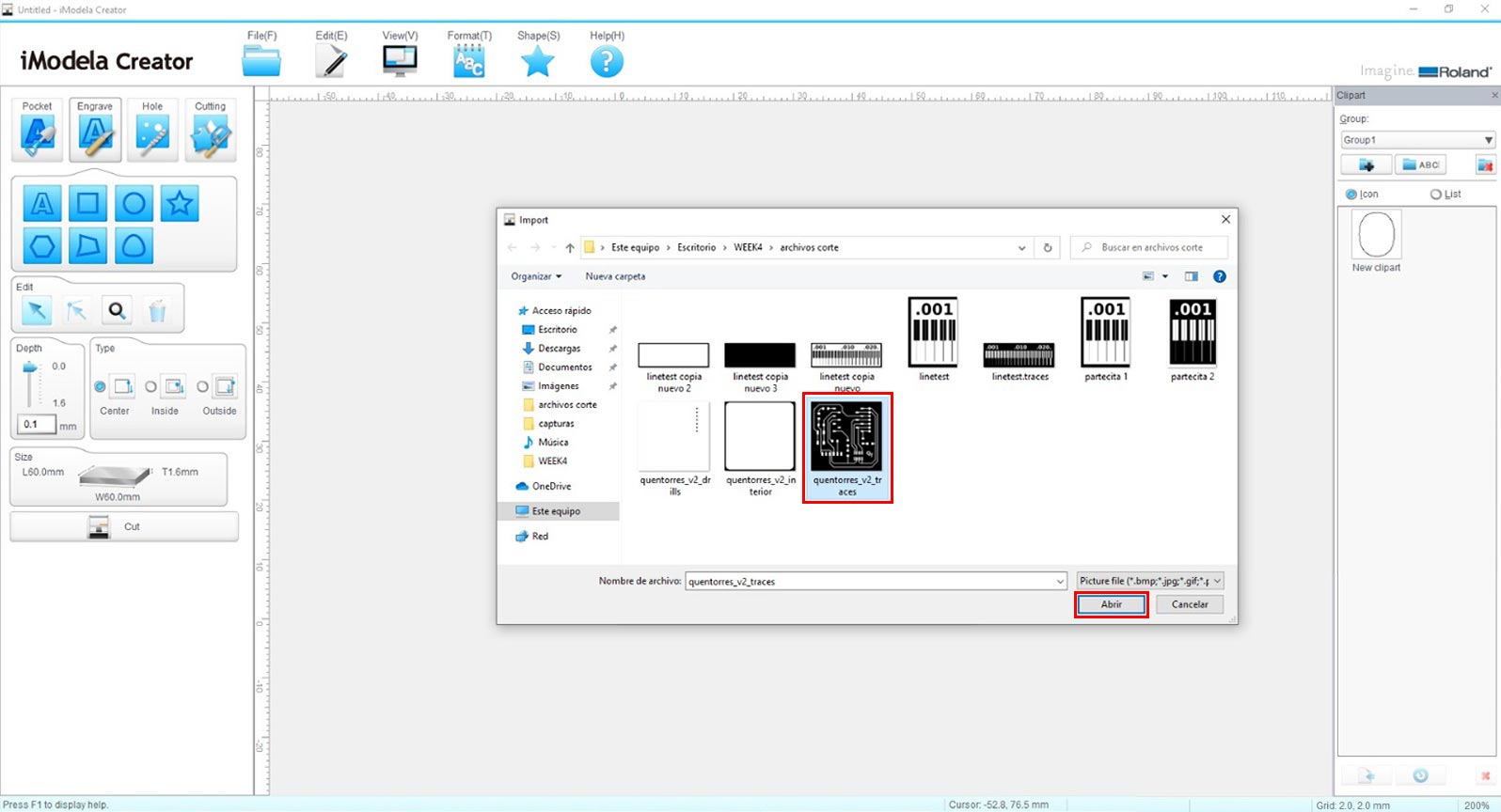
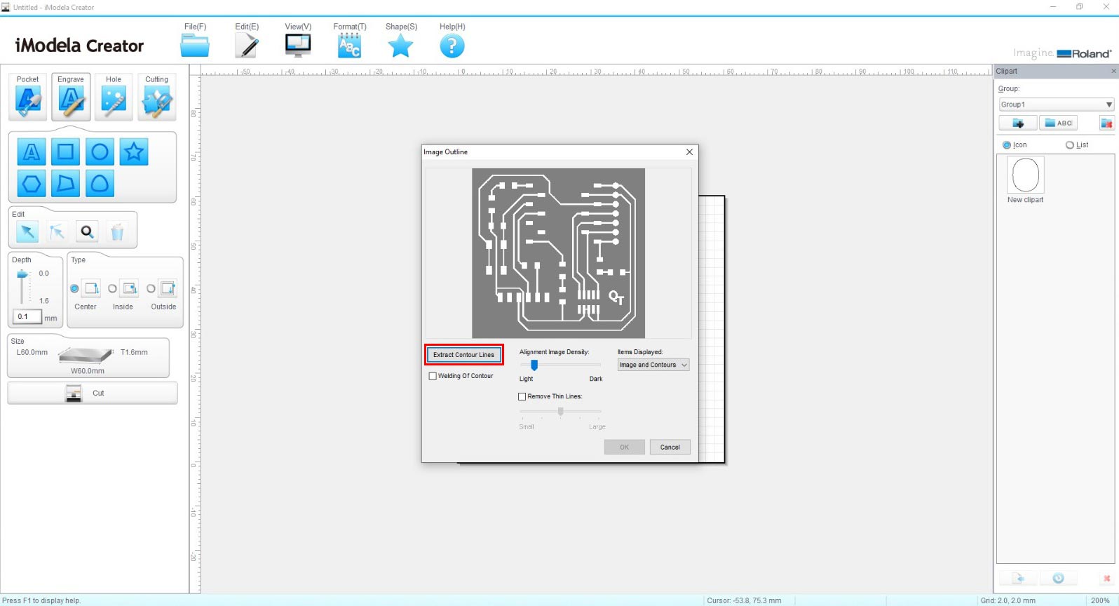
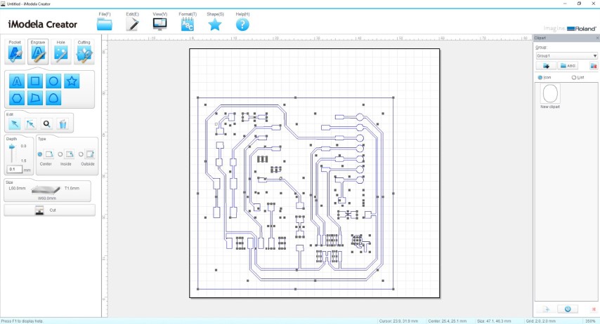
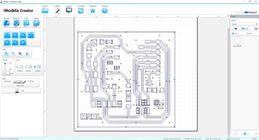
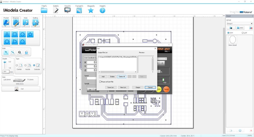
For my individual assignment, I used the parameters obtained previously in the group work to mill the board. First, I downloaded the file, opened iModela Creator and imported the design file. Then, I configured the parameters. Mode: Engrave | Depth: 0.1mm | Type: Outside | Cutter shape: Flat | Blade diameter: 0.4 mm | Milling speed: 90/90 mm/min | Tool down speed: 90/90 mm/min | Cut-in amount: 0.04/0.2 mm | Stepover: 0.20/ 0.10 mm | Finish margin: 0.01 mm.
Configuring traces parameters in iModela Creator
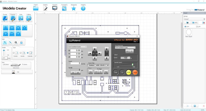
Then, I opened Vpanel, set the origin point for the milling job, loaded and saved the tool path of the design (previously generated in iModela Creator). Finally, I started the milling process.
Configuring Roland VPanel for milling board
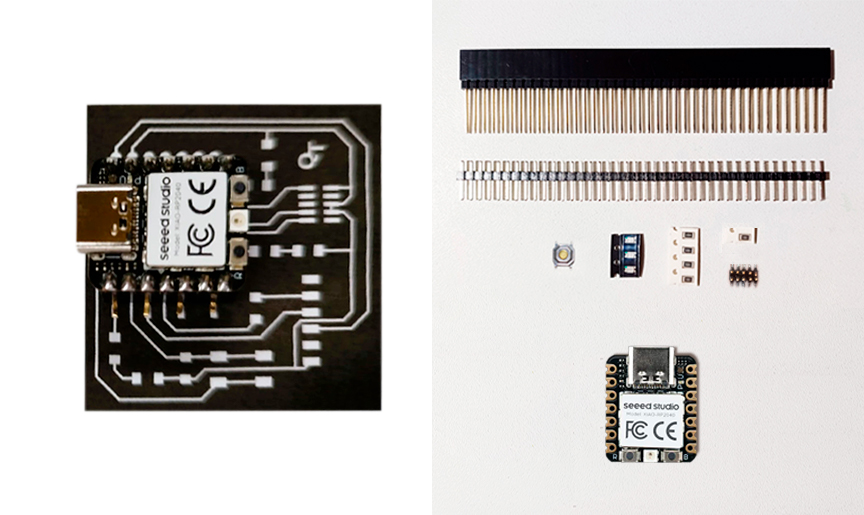
Before sending the board to be manufactured, I make a verification by printing the actual size of the board on paper and placing the XIAO RP2040 on it.
Checking if all the components fit well into the board soon to be manufactured
Modified components to SMD
Having verified the microcontroller fits well, I send the board to be manufactured.
Personalized milled board
Remember that an important tip for the board to come out well is the leveling of the work area of the milling machine.
Soldering Quentorres
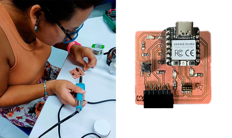
Soldering is the process of joining two pieces of metals using a filler metal, known as solder, that has a low melting point and below the melting point of the workpiece. Soldering is used to form a permanent mechanical and electrical connection between electronic components. In this process, the guidance of Roberto Delgado and the in-person help of my colleague Silvana Espinoza was essential, who helped the entire team of soldering novices.
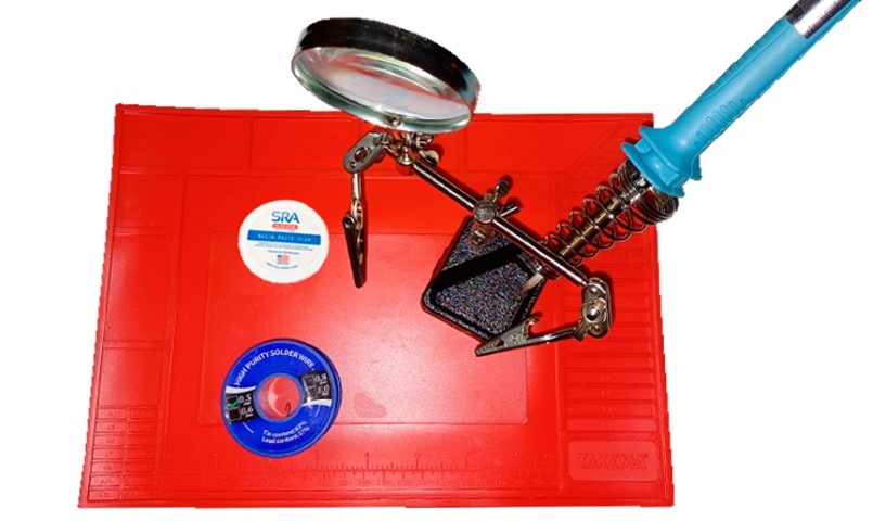
Basic soldering tools and materials:
A low melting point metal (soldering wire).
Heat source (soldering iron).
Flux (prevents subsequent oxidation of welded surfaces).
Soldering tools and materials
Since this is my first time soldering, I bought my own tools and materials to practice at home. I bought everything in Paruro.
Soldering: step by step
To solder you must:
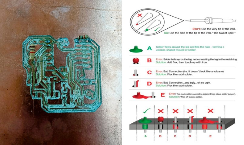
Clean the board: first with brush, then scraped on a piece of MDF (to remove burrs). Then, clean it with 300 grit sandpaper (or the finest). Finally, clean it with isopropyl alcohol.
To start soldering: go over the areas to be soldered with a flux pen.
One side of the printed circuit is tinned.
The component is placed and we count to five.
Apply solder and count to three to remove solder.
First soldering practices
After practicing in a board and with components I will not use, I started soldering the Quentorres board.
Starting Quentorres soldering
After soldering the pieces, continuity must be verified with the multimeter instrument.
Silvana checking the cathode and anode are properly positioned on the board
Finishing solding the Quentorres
Important: wash your hands after soldering to avoid accidental consumption of materials.
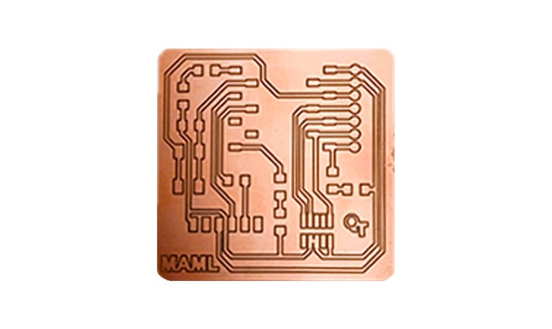
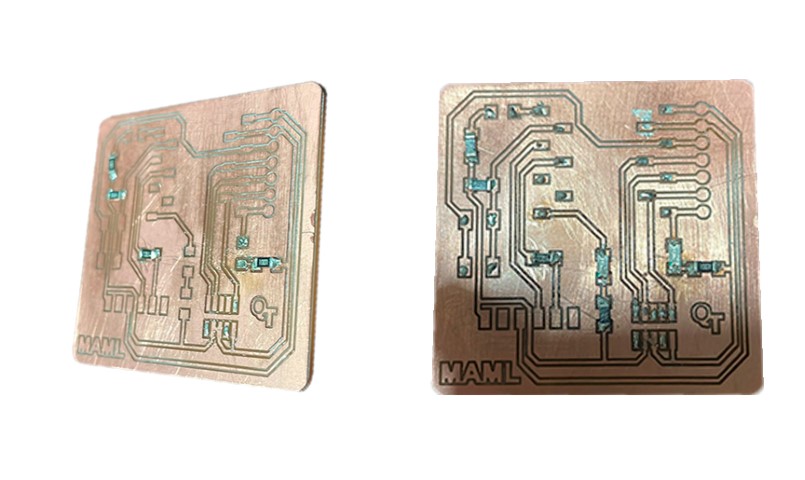
After making the Quentorres seen above, I realized that the name I wrote in it was covered with a component. So I decided to mill and solder a second version:
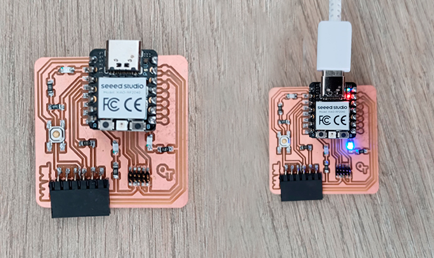
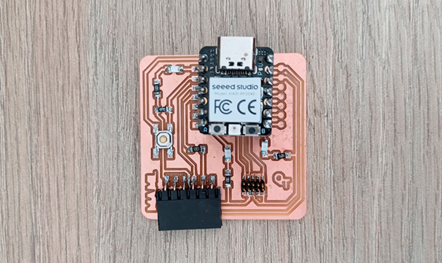
Final Quentorres PCB
Programming Quentorres
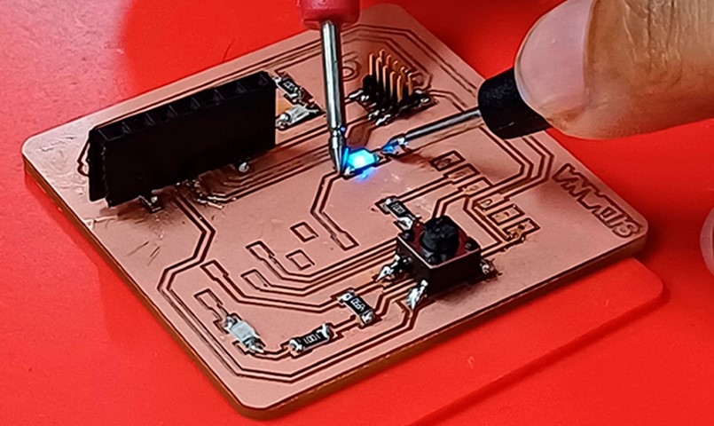
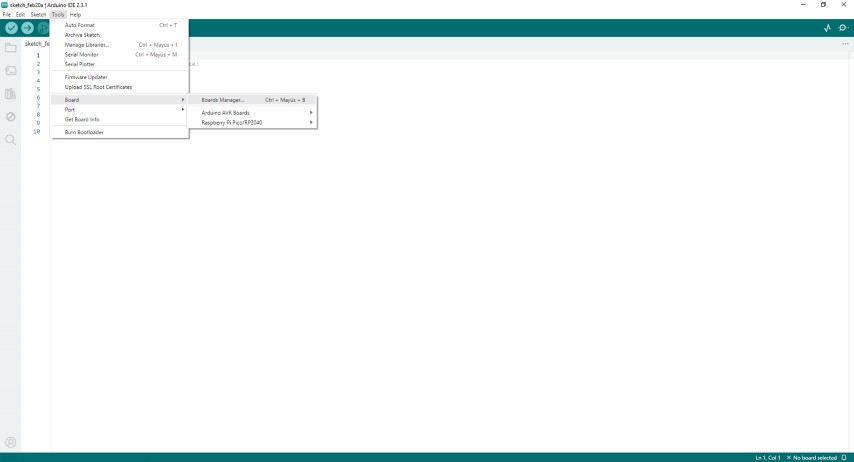
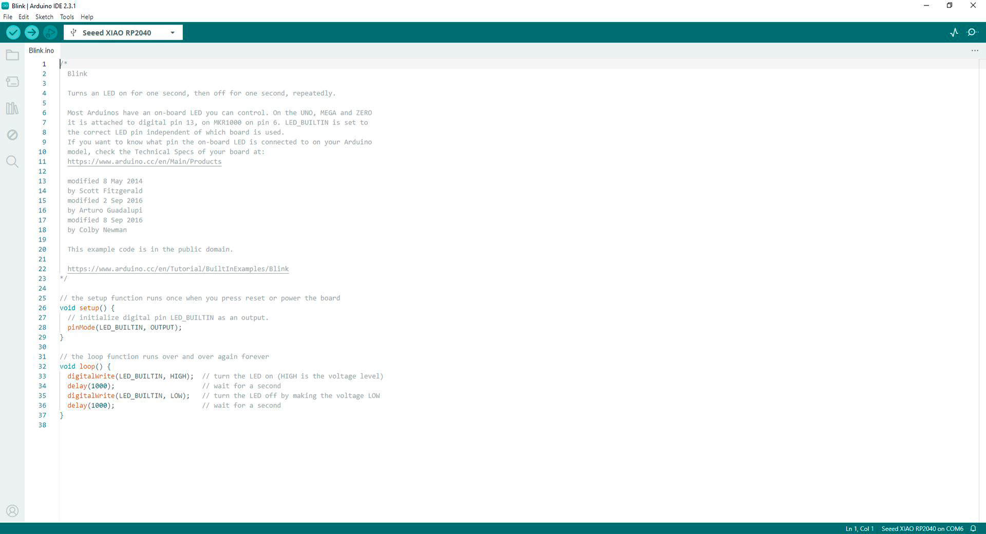
Finally, to check that everything went well, I programmed the Quentorres with Arduino IDE.
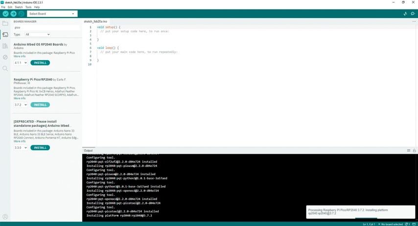
Configuring Xiao RP2040 in Arduino IDE
Once microcontroller Xiao RP2040 is reconigzed by Arduino IDE in port COM6 (this port can change in other computers, except for COM1 that shoul be never selected), I applied a blink example (file-example-basic-blink). For getting the LED in pin D7 to blink I modified the code.
const int ledPin = D7; // Pin D7 on Xiao rp2040

// the setup function runs once when you press reset or power the board
void setup() {
  // initialize digital pin LED_BUILTIN as an output.
  pinMode(ledPin, OUTPUT);
}

// the loop function runs over and over again forever
void loop() {
  digitalWrite(ledPin, HIGH);       // turn the LED on (HIGH is the voltage level)
  delay(1000);                      // wait for a second
  digitalWrite(ledPin, LOW);        // turn the LED off by making the voltage LOW
  delay(1000);                      // wait for a second
}
Modifying the example code in Arduino IDE for getting the D7 pin LED to blink
Once the PCB is programmed, comes the real test: if all the actions previously carried out were correct, the light should turn on.
Programmed Quentorres
After a very intense week of work, my Quentorres worked! For me, these days were a great learning experience because it is the first time I have made and assembled a PCB, almost from scratch (I still need to design the traces, but that is a topic for another week).
Conclusions
In exceptional cases, the deficit in the stock of components can be resolved by modifying the legs of the components that are most abundant where I am. All I need is patience to explain what I need to the seller and a pair of pliers.
Before sending any trace to be milled, do a test. Even in the test, a small unevenness that may exist may not be so clearly evident, so I must always carefully check the board obtained.
The edges of the plate can be very sharp so it is better to work with a rounded edge.
Teamwork was essential this week. Since our team, for the most part, was new to electronics, we divided the tasks. Some were in charge of researching the software to use the milling machine, others went to buy missing components, others helped us and guided us with soldering and programming.