8. Electronics Design
Group assignment:
-
Use the test equipment in your lab to observe the operation of a microcontroller circuit board (as a minimum, you should demonstrate the use of a multimeter and oscilloscope)
-
Document your work on the group work page and reflect on what you learned on your individual page
Individual assignment:
- Use an EDA tool to design a development board to interact and communicate with an embedded microcontroller
Download Design Files
Click here to download my design files folder
Group Work Reflection
For the group work this week, we used a digital multimeter and oscilloscope to observe the operation of microcontroller circuit board. I have been using a multimeter for the past ~2 years in Charlotte Latin School’s engineering classes and felt very comfortable with it. I had used the oscilloscope before to measure different wind turbine’s voltage generation in my Civil Engineering class, however, I didn’t feel very comfortable with my skills with it. Richard Shan and I originally did some basic testing of his board’s LED that was programmed to blink an LED every 200 milliseconds (we used his because it already had a programmable LED connected to pin 4 of the ATTiny412, which is a PWM pin). From this my understanding of the multimeter remained about the same and the oscilloscope I felt I understood better, but still was confident using it.
Later, however, Mr. Tom Dubick provided a wonderful quick-lesson on Analog vs Digital pins, PWM pins, dimming LEDs, and change in voltage on a multimeter (one moment in time) vs an oscilloscope (shows change over time).
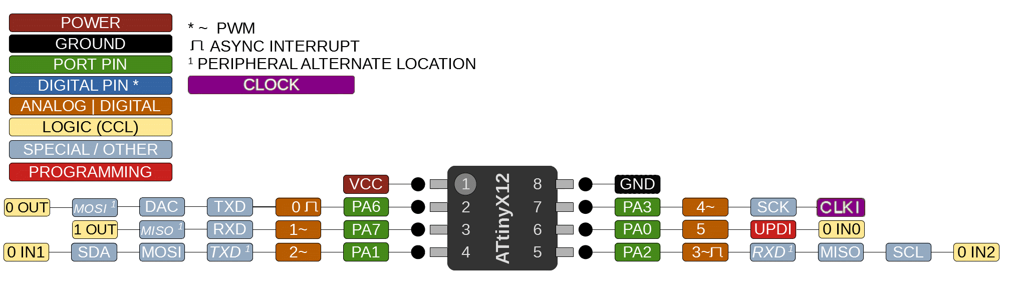
To show change in voltage over time, we needed an LED to dim over time that was connected to a PWM pin on the ATTiny412 (these are indicated by a “~” symbol on the above pinout image). Pins 3, 4, 5, and 7 work as PWM pins. Mr. Dubick recommeneded that I look at a TinkerCircuit for an example code to better understand how to program/what the code means for a dimming LED.

This TinkerCircuit is by 225 Sujiwan Chuyim and can be found with this link.
The following is the code annotated so that I could understand it (note this code directly put into Arduino will not work, use the code in my design files folder):
int ledPin6 = 6;
void setup() {
pinMode(ledPin6, OUTPUT);
Serial.begin(9600);
}

void loop() {
for (int x = 0; x < 255; x++) {    x=0 so where LED light starts out, then, if x is less than 250, x++ which means add one to it)
    analogWrite(ledPin6, x);
    delay(50);
    Serial.println(x);
}
delay(500);
for (int x = 255; x > 0; x--) {     x=255 so LED light tops out at 255, so when LED = 255, x— which means take one away where x is greater than 0
    analogWrite(ledPin6, x);
    delay(50);
    Serial.println(x);
}
delay(500);

}
The x values change depending on the LED being used, so you have to check its voltage.

From this image you can see that the the amount of voltage never changes but rather the time that you can see it changes, fooling our eyes into thinking the LED is dimming.
Designing
1. Board Design #1
The Schematic
To make the schematic I started by watching this tutorial and reading this article. Next I downloaded the symbols library by going to preferences > manage symbol libraries and then clicked on the folder icon, selected the library I wanted to add, clicked ok, and then clicked ok again. I then opened a new project in KiCad’s schematic editor. I started by using the Add symbol (A) tool to add components. I added an ATtiny412, a 1206 LED, a 1206 capacitor, a 1x6 conn pin header, and a whole bunch of 1206 resistors. I clicked the Add a wire (W) button to activate the wire tool. By clicking on pins of the components, I could click and drag my cursor to connect component pins. I then just fumbled around until I finally made something that resembled a working schematic. I kind of resembled my board after the button blinky board Teddy Warner talks about in his week 6 Fab Academy 2021 documentation. I also used the ATtiny pinout from sheek geek to help decide how to wire the board.

Additionally, I considered how the board would connect to my Quentorres board I made during week 4. I used this Seeed Studio XIAO RP2040 information and pinout image to ensure my wiring would work.

The schematic:

PCB Editor
First I needed to download the footprint library. I went to tool > assign footprints > preferences > manage footprint libraries. I then clicked the folder icon, selected the footprint folder I wanted to download, clicked ok, and then clicked ok again (Note that if the footprints don’t appear at first you may need to close and reopen KiCad again).
Next, I needed to route the traces. My first step was to organize the rats nest.
First, I moved the footprints into similar positions as their corresponding symbols in my schematic. I then selected the route tracks tool and clicked where I wanted the wire to go. - While routing my traces, KiCad helped me visualize where my traces could and could not go by not allowing me to touch a trace to another (unconnected on the schematic wiring) trace. Thus, I had to be thoughtful and kind of put together a puzzle while routing. I prefer doing the routing process myself as opposed to auto routing because, for one I did not know about it until way too late into my design process, and two, I like the routing process. It took a lot of trial and error until I finally found a way to route all of the traces properly and then even more trial and error to clean it up as best I could. The PCB design is pictured below:
I also had to control click, click the selection button, uncheck the boxes besides the tracks box, click ok, control click again, and the click the properties button and specify my track width as 0.5 mm. Previously, the track width was set to 0.2 mm and was extremely fragile so increasing the size was very helpful for the longevity of my boards!

The Outline
For now I just made a white box as the outline as pictured earlier in the PCB Editor image. I used the “Draw a rectangle” tool in the PCB editor. I later plan to try making a more unique board shape!
2. Board Design #2
This week’s work conflicted with my school’s spring break so we had to work at home for the first half of the week. After we returned, I realized my first board design was missing features it needed to have.
The Schematic
After talking to Evan Park, I realized there was a much easier and neater way of wiring my schematic: global labels. By clicking the Add global labels button and entering a name in the global label properties popup, I was able to then click to place a label. The label acted just like a component would in that I could use wires to connect it to other pins or just simply drag it close enough to other components’ pins that the pins touched eachother in the schematic. I could then copy and paste the label and connect it to another pin and KiCad would recognize that as the pins being connected/wired to one another. I like the global labels for helping better organize and de-clutter the schematic.
I took the original file and messed around with it until I settled on the following image:

I used many global labels in my design to clean up the overall appaerance of the schematic.
In the top left is the LED indicator. This will make it so that, when I plug the board in, the LED will turn on as an indicator that the board works. This will save us from the hassle of using the multimeter to check if the board works.
Below the LED indicator is the Button’s wiring.
Below that is the PWM-Programmable LED so that, if I wanted to, I could program a dimming LED.
Below that is the wiring for the header that will connect the output device, an OLED, to the board.
In the bottom right is the wiring for the header that will connect the limit switch (an input) to the board.
And in the top right is the ATTiny412 and its wiring.
PCB Editor
I followed a similar process as for the first board to wire the traces for this board.

I ended up using a lot of 0 ohm resistors to make this board possible. It wasn’t until after I milled the board that I learned that the surplus of 0 ohms was undesirable so I will later try to make another board without the 0 ohms.
The Outline
Again, I made a white box for the outline, however, I am going to experiment more in the future with board shapes and designs!
Customization
I wanted to try engraving my initials “AD” with “Fab Academy” below them and some stars to the text’s right. For the initials, I used the Text tool in the PCB editor, typed “AD,” kept the KiCad Font, set the width to 3mm, height to 1mm, and thickness to 0.2 mm. I then changed the layer type to “F.Silkscreen.” I then hit OK and clicked on the PCB design to place the text. I followed the same process for the “Fab Academy” text only the width was 1mm, height 0.5mm, and thickness 0.1mm.
For the stars I first found an image online I liked. I downloaded the image, put it into remove.bg to get rid of the background, converted the file to a .bmp (bitmap), and then opened it in KiCad’s Image Converter. I scaled the image down so that it was 1.27mm x 1.27mm, toggled the black/white threshold until I got the clearest image, set the output format to “Footprint (.kicad_mod file),” and then exported it to clipboard. I then opened the PCB editor and clicked to place the star’s footprint.
Here you can see the board in KiCad’s 3D Viewer:

3. Blink Board
The Schematic

PCB Editor

The Outline
Again, I made a white box for the outline as seen in the PCB image above.
4. UPDI Connector Board
For more easily connecting the blink board to the Quentorres, I needed to make this UPDI Connector Board.
Angelina Yang and Kabir Nawaz had found this UPDI connector board as a .png on the Fab Academy schedule for this week and, with their help/documentation, I milled this board.


Milling
I used the same workflow as I did in week 4’s electronics production milling.
- Note: The board milling process described here is for Board Design #2, however, the same general processes is followed for the milling of all of the other boards detailed in this week
Material Setup
installed the 1/64” bit first
Material Size:
-
X = 127mm
-
Y = 102mm
-
Z = 1.9mm
-
The Z value is obtained from probing the material, I clicked “Material Offset Probinh Routines” and followed the instructions that popped up to get the Z value.
Material Placement:
-
Material Offset Z = 0.01mm
-
Alignment = Left and Front
File Setup
I imported two files to the PC connected to the milling machine: “board 2-Edge_Cuts.gbr” and “board 2-F_Cu.gbr”
Edge Cuts Settings:
Milling Tools:
- 1/32” Flat End Mill
Toolpaths:
-
Side to mill = Top
-
Outline
-
Trace Depth = 0.15mm
-
Trace Clearance greater than or equal to 1.5mm
-
Rotation = 0 degrees
I then clicked “Generate G-Code Now”
“board 2-F_Cu.gbr” Settings:
Milling Tools:
-
1/32” Flat End Mill
-
1/64” Flat End Mill
Toolpaths:
-
Side to mill = Top
-
Traces
-
Trace Depth = 0.15mm
-
Trace Clerance greater than or equal to 1.5mm
-
Rotation = 0 degrees
I then clicked “Generate G-Code Now”
Plan Setup
Edge Cuts Settings:
Plan Offset:
-
X = 5mm
-
Y = 53mm
-
Z = 0mm
“board 2-F_Cu.gbr” Settings:
-
X = 8mm
-
Y = 55mm
-
Z = 0mm
After changing the positions of the files, I had to go back to the file setup tab and re-generate the g-codes.
Summary/Run Job
I clicked “Mill All” and then watched the milling to ensure everything ran smoothly.
The Milled Board:

The customization design did not end up in my final milling due to time constraints and needing to be done ASAP before the lab closed, however, I plan to try fun designs on future boards!
Blink Board Milling Problem
When milling the blink board, I had very bad luck and had two bad bits. The following image shows, in order from left to right, (1) the good mill, (2) the first bad mill, (3) the second bad mill:

Image of the good blink board milled:

Soldering
Board #2
Bill of Materials
-
2 x Female Conn Header 1x03
-
1 x Female Conn Header 1x04
-
1 x 970nF capacitor
-
4 x 499ohm resistor
-
2 x 1206 Blue LED
-
1 x ATTiny412
-
1 x Button
-
12 x 0ohm resistor
The final soldered board:

I connected board 2 to my quentorres board and the quentorres board to my laptop and the LED indicator on board 2 turned on, indicating that the board works!

Blink Board
Bill of Materials
-
1 x Female Conn Header 1x03
-
1 x ATTiny412
-
1 x Button
-
1 x 970nF capacitor
-
2 x 499ohm resistor
-
2 x 1206 Blue LED
-
2 x 0ohm resistor

UPDI Connector Board
Bill of Materials
-
1 x 6-pin male header
-
1 x 3-pin female header
-
1 x 4.99 ohm 1206 resistor

Programming Board #2
Arduino
After a lot of trial and error, I finally managed to program an LED on my second board with the Arduino.
void setup() {
// initialize digital pin LED_BUILTIN as an output.
pinMode(6, OUTPUT);
}

// the loop function runs over and over again forever
void loop() {
digitalWrite(6, HIGH);   // turn the LED on (HIGH is the voltage level)
delay(1000);                       // wait for a second
digitalWrite(6, LOW);    // turn the LED off by making the voltage LOW
delay(1000);                       // wait for a second
}
In Arduino 1.8.18 I opened the example “blink” code and altered “LED_BULITIN” to be the pin connected to my LED, pin 6. I then selected Tools > Programmer > Atmel JTAGICE3 (JTAG mode). Next, I selected Tools > Port > COM17. I then uploaded the above code.
Although this was a good sign that my board is programmable, the LED that I programmed/is blinking in the video is my LED indicator… not the LED I intended to make blink. I then was confused about what pin my other LED was connected to and referenced the ATTiny412 pinout image. My LED should have been connected to the pin I thought it was and I got very frustrated… I eventually tried every pin (1-8) in the blink code and uploaded it but non of them worked.
At this point I decided to be happy with the fact that I did program an LED to blink and decided to move on to trying to do so again with the Quentorres board.
Quentorres
Unfortunately, the board broke o_o
So, I decided that, the board was already a wreck so, instead of leaving future goals for electronic designing in the future, I would just make a new, better board that would make my life easier with less potential problems within it. (This is when I then made the Blink Board and then UPDI Connector Board.)
(Previous) Future goals:
-
make a board with a maximum of 1-2 0 ohm reistors, really try to avoid using them in the future by doing one of the following:
-
instead of having one board that has an OLED (output), limit switch (input), and have a programmable LED/button, design, mill, and solder multiple boards to achieve the same purposes
-
have more than one ATTiny412 on the one board to minimize the clustering of traces to one single spot’s pins
-
making a board with multiple layers or a board with traces/components on its front and back
Programming Blink Board
When programming the blink board, I checked that it worked first by seeing that I could turn the LEDs on with an Arduino and then moved straight to programming with the Quentorres.
Quentorres
I connected the blink board to the Quentorres through the UPDI Connector board as pictured below:

I then uploaded the same code as before to program the LEDs to blink as shown in the video below:
Problems Encountered
The majority of the problems I faced this week was just being unfamiliar with the software, terminology, and desired result. It just took a whole bunch of clicking random things to finally get a feel for what I was doing. I really think my biggest problem was not even knowing where to begin; for example, if I had pin outs for a LCD, what pins do I need to have on the RP2040 for the LCD pins and how do I know what LCD pins need what RP2040 pins? A lot of questions such as these were my biggest problems as I didn’t quite know how to even phrase or ask the questions I had. Thankfully, when we were back in the lab, I was able to talk with my lab mates and collectively we were able to start to understand what we were doing.
Other than just not knowing how to design a board, I had no problems with my designs working.
Reflection
This week was rough. With it falling over my school’s spring break and not being able to go into the lab and collaborate with my classmates, it was super challenging. Furthermore, I (unfortunately) got the stomach flu during this week which really set me behind. This week mainly taught me to trust the process, take your time (understanding concepts wise), and prioritize feeling better first, then grind and kill your fab academy work!
References
http://fabacademy.org/2020/labs/oulu/students/noora-nyberg/assignments/week09/
https://www.youtube.com/watch?v=pgKfaFI4T4Y&list=PLn6004q9oeqGl91KifK6xHGuqvXGb374G&index=3
https://teddywarner.org/Projects/VonNiemannProbe/#pcb-design-integration
https://docs.kicad.org/6.0/en/getting_started_in_kicad/getting_started_in_kicad.html
https://gist.github.com/exocode/887ee367f9a0df89f3fd2b2e27317919
https://fabacademy.org/2024/labs/charlotte/students/angelina-yang/assignments/week09/
https://fabacademy.org/2022/labs/cpcc/students/garrett-nelson/assignments/week07/
http://fabacademy.org/2021/labs/charlotte/students/theodore-warner/Assignments/week06/
https://docs.google.com/document/d/1mdS0UQ5VlbT6YqfHQQTiP2TreoGWLNhuN62La5mOJcE/edit?usp=sharing
https://wiki.seeedstudio.com/XIAO-RP2040/
https://www.instructables.com/Understanding-the-Pull-up-Resistor-With-Arduino/
https://fabacademy.org/2021/labs/waag/students/nadieh-bremer/blog/week-13/
https://fabacademy.org/2021/labs/waag/students/nadieh-bremer/blog/week-6/