Final Project
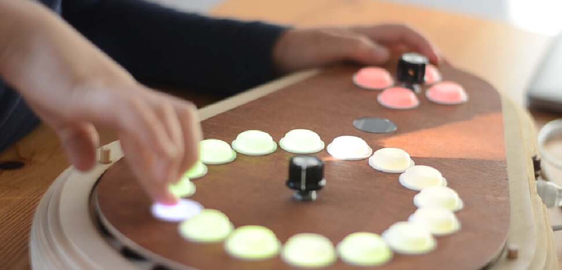
Final project Initial conception (Febuary 2022) Learning to play any musical instrument takes a very long time and a lot of effort. To enjoy music …
Electronics production is an important skill in the FabAcademy. It’s interesting that in even precedes any other electronics based skill. It is taught before electronics design and embedded programming. This is opposed to many traditional electronics courses where you first have to deeply invest in learning how a breadboard works and how Ohms law should be applied. FabAcademy skips a lot of steps but I think students will eventually have better ways to quickly prototype their electronic ideas. I will definitely keep this in mind when designing my own courses. One downside though may be for some students to find it hard to work on things they don’t fully understand yet. A sentence like:
“You need the SAMD11, which has to be programmed using the SWD JTAG programmer, and a UPDI adapter board to program an Atiny AVR.”
can be a bit daunting if you don’t actually know what you’re making. Also, I like the notion of skipping through-hole components all together. This makes PCB creation a lot less time consuming and makes a lot of components more accessible.
I started making my own electronics just around the time when the Arduino became popular. I had an etching installation in my student bedroom and did all kinds of bread-boarding experiments. I made some PCBs but abandoned the practice in favor of ordering them from a board house, since that became very cheap. A year ago I ordered a 3018 mill in order to make my own PCBs again because the delivery times of PCB manufacturers wouldn’t allow me to iterate fast in designing electronics. I had little success with the 3018 and it has been collecting dust for over a year now. This week’s assignment would allow me some time to see if I could get that 3018 mill in working order and be able to produce satisfactory PCBs at home as well as in the Fablab.
My goals for this week were:
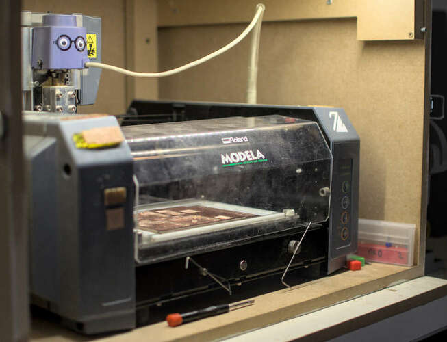
The milling machine at the Waag (Fablab Amsterdam) is the Roland MDX-20. It is being controlled by a PC running Ubuntu Linux. The “mods” application is used for he entire workflow.
 |
 |
|---|---|
| The Roland MDX-20 | It is watching us… |
Here’s an overview of the workflow for milling the traces of a PCB:
| Preparing the control-software (mods) | |
|---|---|
| Open mods in the terminal. This starts a local webserver, a websocket-to-serial service to control the mill and a web-browser with mods loaded | |
Connect to the correct websocket and the serial port in the WebSocket serial module. |
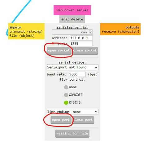 |
| Load a PNG file that represent the traces on the board. | 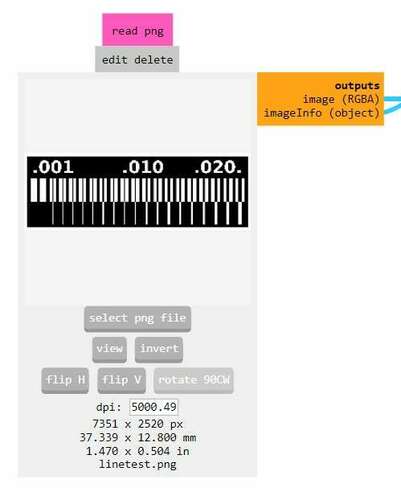 |
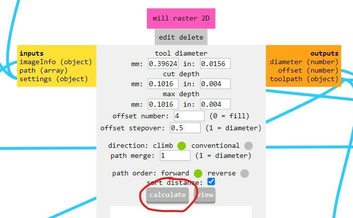
In the set PCB Defaults module, change default cut depth (1) to 0.002inch for min and max. Don’t forget to press mill traces (1/64) (2) to copy settings to mill raster 2D. |
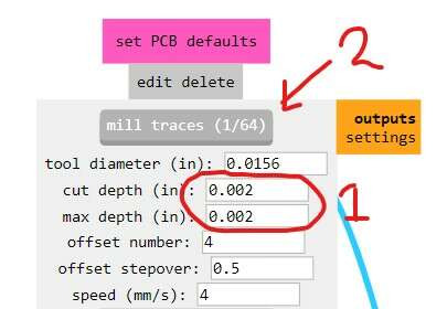 |
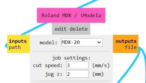
In the Roland MDX/iModela module, set cut-speed. We set it to 3, because we experienced there was a smaller chance of breaking the milling-bit. |
 |
Press calculate in the mill raster 2D module |
 |
| Preparing the PCB and mill the traces | |
|---|---|
| To prepare a milling job, place a blank PCB onto the sacrificial plate. | 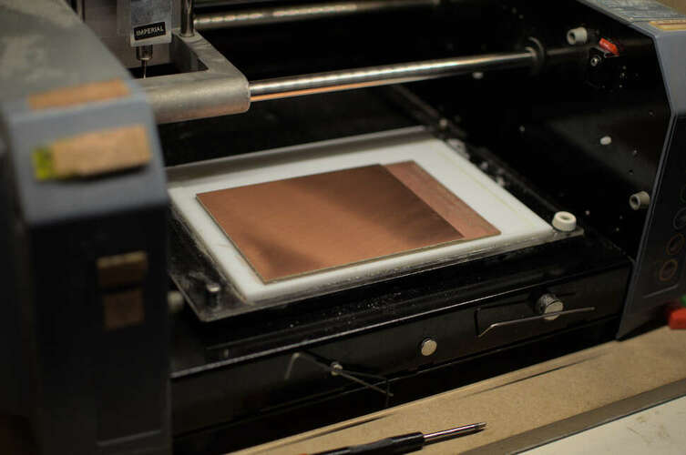 |
| Be sure to secure it with double sided tape | 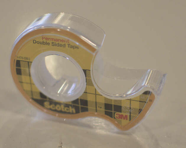 |
| Insert the 0.4 double-flute milling bit into the holder. Be careful not to drop it. Even dropping it from 10mm height it will break the tip. | 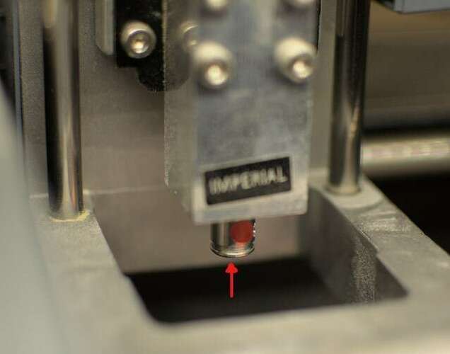 |
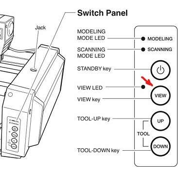
Press the view button on the mill to put the mill into view mode. Press it again to home x and y to 0, 0 |
 |
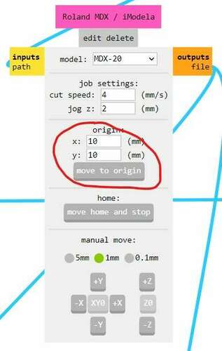
Enter homing coordinates into the Roland MDX/iModela module so the mill is in the lower-left corner of the area to mill. Press move to origin when ready. |
 |
Lower the z-axis with the up and down button on the mill so it is at around 5mm above the pcb |
 |
| Loosen the milling bit and gently place it on the surface of the pcb. Apply slight pressure to ensure the tip of the mill is exactly on the surface. Then tighten the milling bit. | 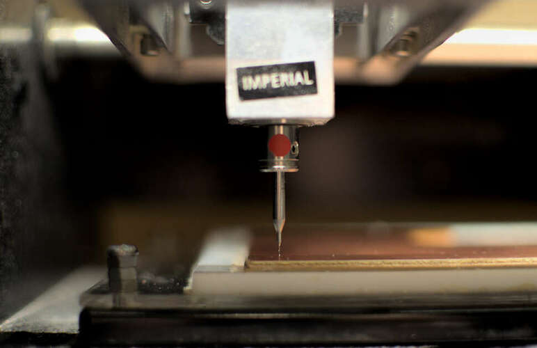 |
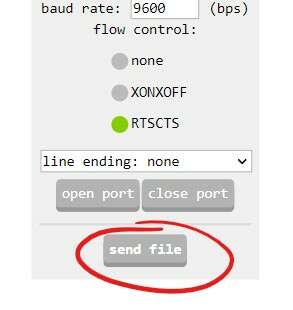
In the WebSocket serial module, press send file to start the machine" |
 |
| Wait for the job to be finished. |  |
| When the job is finished, vacuum the dust from the PCB | 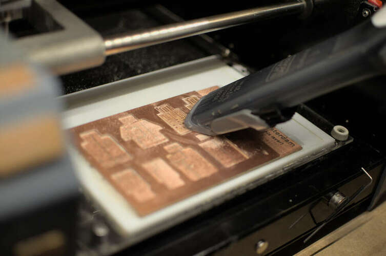 |
| Mill the outline | |
|---|---|
| Raise the z-axis using the buttons on the milling machine | |
| Change the milling-bit to the 0.8mm milling bit. | |
| In mods, load the PNG for the outline of the board | 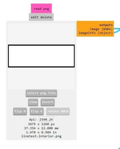 |
| Set the min cutting depth to 0.4mm (half the milling bit diameter) and the max cutting depth to 1.55 | 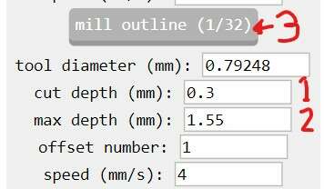 |
The cut-speed can be set to 4mm/s in the Roland MDX/iModela module |
|
Press calculate |
|
Press the view button on the mill to put the mill into view mode. Press it again to home x and y to 0, 0 |
|
Enter the Origin coordinates used when milling the traces. Press move to origin when ready. |
|
In WebSocket serial, press send file to start the machine" |
|
| Wait for the job to be finished. | |
| When the job is finished, vacuum the dust from the PCB | |
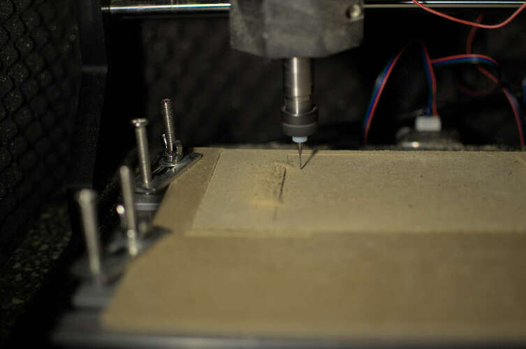
| Lift the finished PCB from the plate using a screwdriver |
| If the milling job fails | |
|---|---|
| Cancel the job in “mods” | |
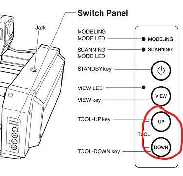
| To make the mill “forget” the commands already sent to it, press Up and Down simultaneously for about 10s | |
Enter the Origin coordinates used when milling the traces. Press move to origin when ready. |
|
Make sure to write down the origin coordinates when starting a job. This information gets lost when mods crashes or something else happens.
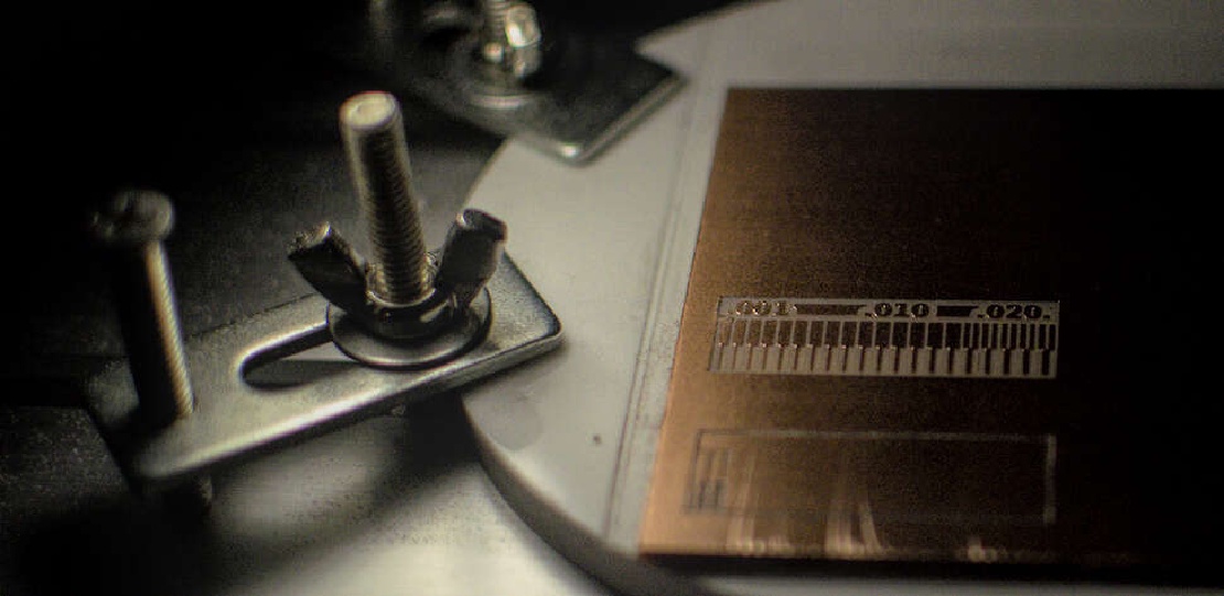
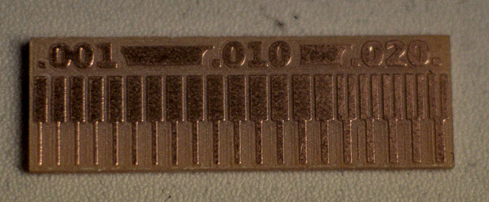
To get to know the Roland MDX we had the assignment of milling two boards, one with a one-flute mill and one with a two flute mill. Both boards were milled with the following settings:
| Parameter | Traces | Outline |
|---|---|---|
| Tool diameter | 0.4 mm | 0.8 mm |
| Cut depth | 0.05 mm | 0.6 mm |
| Max depth | 0.05 mm | 1.55 mm |
| Offset number | 4 | 4 |
| Offset stepover | 0.5 | 0.5 |
| Cut speed | 4 mm/s | 4 mm/s |
| Two linetest boards were milled. |
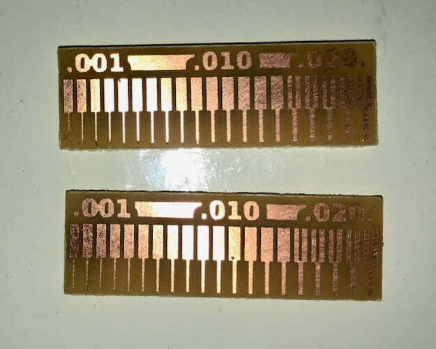 |
|---|
| The top result was milled with a 1-flute mill, resulting in rough edges and traces coming loose from the board. The bottom result was milled with a 2-flute mill and showed superior quality. |
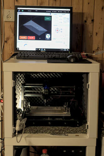
Having learned a lot from milling PCBs at the Waag, I took quite a bit of time this week to tune my 3018 cheap Chinese milling machine.
 |
|---|
| I have set it up in my attic and built an enclosure from a LACK table, MDF wood and noise dampening foam. It’s being controlled by an old Windows PC but that’s probably going to change. |
Time only allows me to summarize the things I learned from the whole process.
| Fabacademy and the Waag were very valuable in perfecting my home PCB milling facility | |
|---|---|
| Previously I used FlatCAM to generate the tool-path and Candle to send GCode to the machine. Flatcam has many features and can be a bit cumbersome to use. Candle is very nice but isn’t very intuitive when it comes to homing. I changed my workflow to “mods” for toolpath generation and and GSender to control the machine. | |
| Use FR1 material instead of FR4. It’s slightly harder to find. I found mine on Amazon | 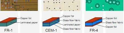 |
| Using an end-mill instead of a v-shaped bit greatly enhanced the results. V-bits are less fragile and therefore seem more attractive to beginners. Especially when you have to figure out the workflow. End-mills are more predictable because the diameter of the tool doesn’t depend on the depth of the cut. | 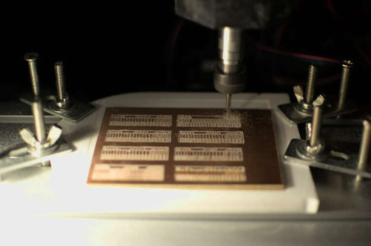 |
| To home the z-axis, this machine has the function to probe the PCB with it’s milling bit. | 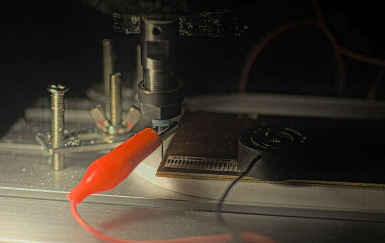 |
Instead of using the probe to scan the entire surface and correct the z-height during milling, like Candle does, I used the Surfacing feature in the GSender software to create a machine-flat surface. First from an MDF bottom-plate but later from a piece of acrylic |
 |
| Use proper workplace “hygiene”. Have a proper place for all the tools. I really liked the way “de Waag” keeps track of all the tools that are part of a certain machine. Magnets hold the important drill-bits and hex-keys. Double-sided tape is hanging on a peg on the inside of the machine enclosure. Facilities like this greatly help optimizing the workflow an reducing frustration | 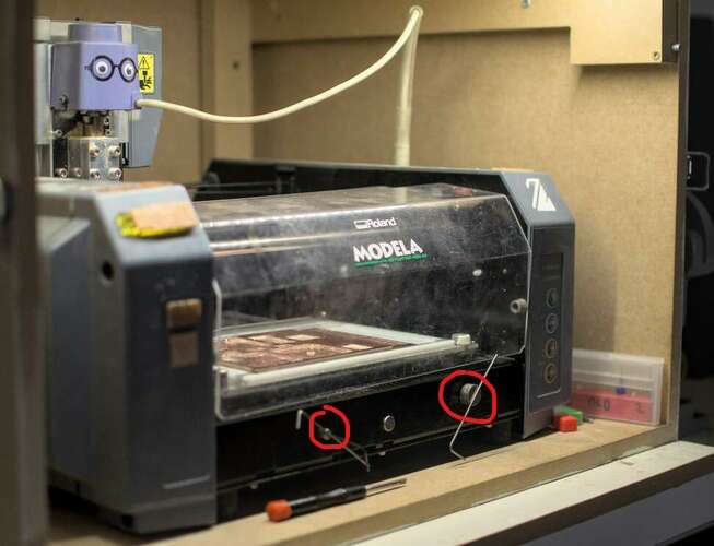 |
| Parameter | Value |
|---|---|
| Milling bit diameter | 0.4mm |
| Feed rate | 1.5mm/s |
| Spindle motor speed | 17000rpm |
| trace cut-depth | 0.002inch |
| perimeter drill diameter | 0.8mm |
| perimeter feedrate | 2mm/s |
| perimeter min. cut depth | 0.3mm |
| perimeter max. cut depth | 1.55mm |
 |
|---|
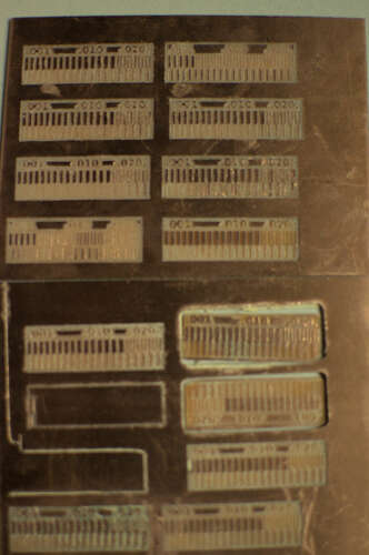
| Insisting on using a v-bit I generated a lot of line-tests |
 |
|---|
| First time abusing a 0.4mm drill-bit to mill |
 |
|---|
| I couldn’t reproduce the quality, but knowing it was possible motivated me to keep trying. I found out the machine had some loose bolts. After fastening them and trying again, the results could finally be reproduced. The third version of this FabISP is probably usable. |
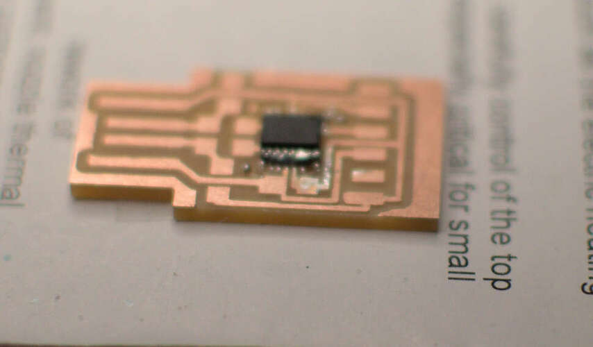
As a first PCB to mill I chose the FTD230SX board, as it would be easy to test whether the board would work or not. The pins on the IC on the board are quite close together so soldering might be a bit of a challenge.
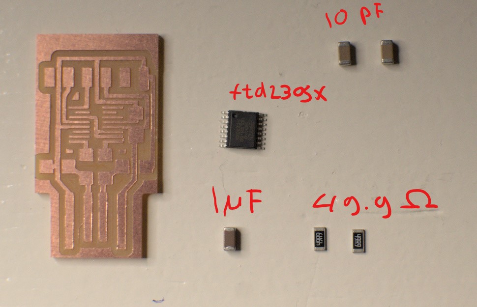 |
|---|
| I sourced the components from the extensive collection of parts at de Waag |
 |
|---|
| As a strategy to solder the part I chose to purposefully bridge the pins to later remove excess solder and have the brides be removed while still having the pins soldered to the board |
 |
|---|
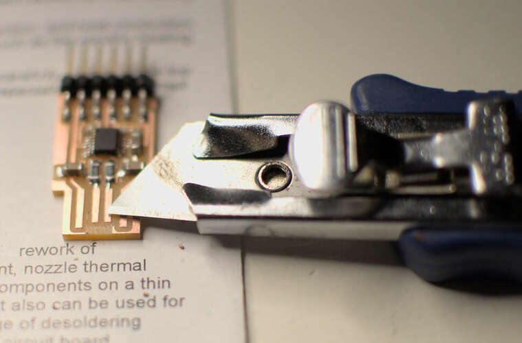
| After soldering I removed copper traced with an exacto-knife. These would otherwise short my USB connection |
The board didn’t work. Having inspected the soldering work under the microscope (some shoddiness detected but also repaired) I couldn’t find any errors. The board was powered with 5v, the 3.3v line measured 3v. Out of ideas, I decided the FTD230SX IC was faulty, so I replaced it.
 |
 |
 |
|---|---|---|
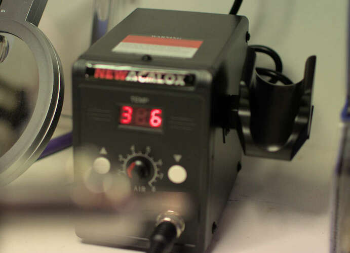
| Using a heat-gun… | …I managed to lift the IC from the board… | …and remove it |
After soldering a new FTD230SX IC, checking all the connections, using a multimeter and a microscope, I still had no result. My MacBook Pro and Linux pcs in the lab could not find my board. I decided to create an entirely new board. The second board also did not work. It got very hot and even a spark was visible. We decided it was probably the flux still on the board that made a short. The IC was internally shorted, as the multimeter proved, so I decided to replace the IC. Again. Still no result.
 |
|
|---|---|
| Having two unusable boards I noticed that some capacitors in the 10pF capacitor collection looked differently | Measuring the value of the supposed 10pF capacitors gave a result of 1uF, a value 1000000 times larger |
Replacing the capacitors didn’t make the board work. The IC was probably already dead because of the charged capacitors. Even if the IC wasn’t dead, the capacitors would have made it impossible for the high-frequent USB signal to ever reach the IC from the laptop.
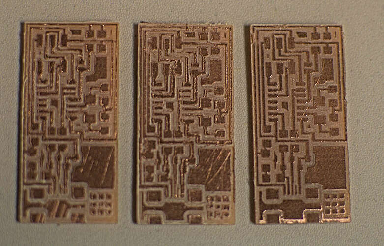
After a day of trying to make the FTD230SX board work, I decided to mill two other boards and populate them at a later time.
 |
|---|
| The SWD JTAG board and the SAMD11 USB-to-Serial board are still waiting to be populated. |
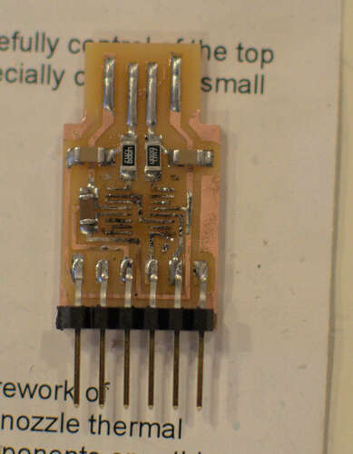
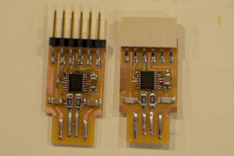
Later in the cycle, instructor Quenten Bolsee discovered the SAMD11 is able to register itself as having two USB serial ports. This resulted in a board that containing two FTDI compatible pin headers acting as two separate serial interfaces.
 |
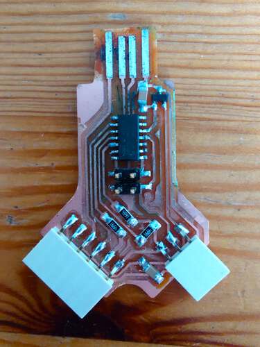 |
|---|---|
| A typical application of this board is that it can act as a UPDI programmer, as wel as a regular serial port, using only one USB port | Student Benjamin Doerig designed and built a variation of this board, having the UPDI programmer already built in |
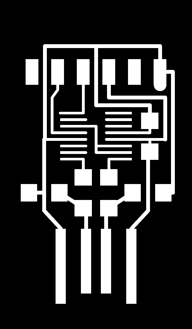
After some mishaps with importing .svg files directly into mods I realized I like using .png files better. It often takes quite some manual labour to convert .svg PCB designs to useful .png files, so I automated the process slightly using a shell script.
This script will take the base filename of your copper layer and outline .svg files and generate two png files. One for the copper traces and one for the outline.
>./svg2png.sh ws2812_button

Background RRGGBBAA: ffffffff
Area 0:0:60.768:60.768 exported to 633 x 633 pixels (1000 dpi)
Background RRGGBBAA: ffffffff
Area 0:0:60.768:60.768 exported to 633 x 633 pixels (1000 dpi)
For basic boards the script will automatically fill the edge circumference but for non-rectangular outlines it is best to do a floodfill manually using a bitmap editor. The script uses the command line interface of InkScape and ImageMagick.
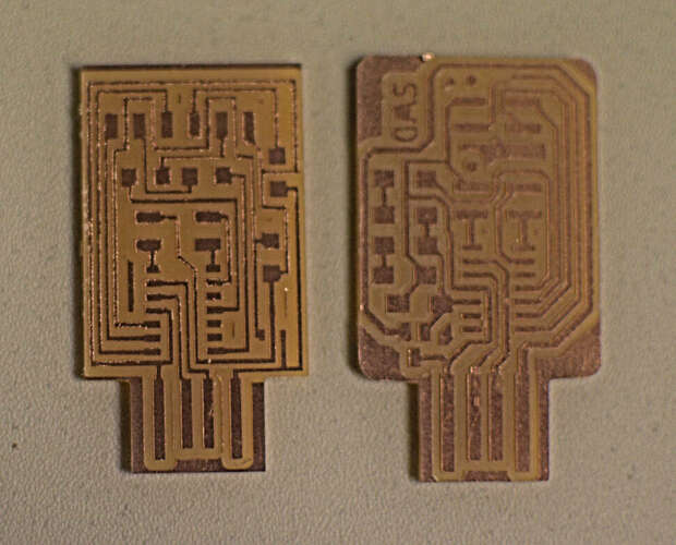
Later in the cycle I needed a quick way to duplicate multiple board designs into one bitmap so they can be milled in one session. This resulted in the script panalize. The script is a bit more complex than I thought it would be, as ImageMagick only supports making a contact sheet of multiple different images but won’t copy one image multiple times. panalize is used as follows:
> ./panelize.sh ws2812_button 2 3
This command will take the outline and the trace files for the pcb files with the name ws2812_button and make two new bitmaps with the images copied in two columns and three rows:
 |
 |
|---|---|
| The outlines… | …and the traces duplicated in a 2x3 grid arrangement |
The process of programming the SAMD11C based USB serial boards is described in the Week 8 - Embedded Programming Documentation.
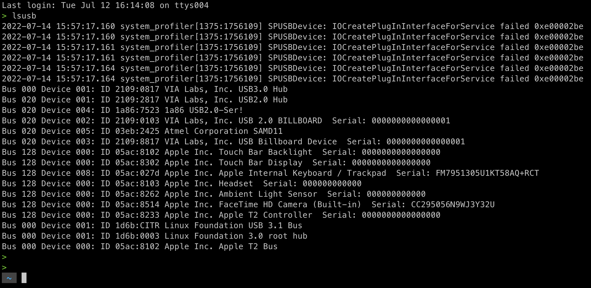
To program any Attiny by any method, first the SAMD11 serial adapter must be recognized. To quickly list the available USB connected devices I use a command-line program called lsusb.
Using the Arduino environment and the MegaTinyCore libraries it is possible to program a lot of new AtTiny boards using the Arduino environment.
 |
|---|
| Using a simple adapter to the USB-serial board, any Attiny can be programmed |
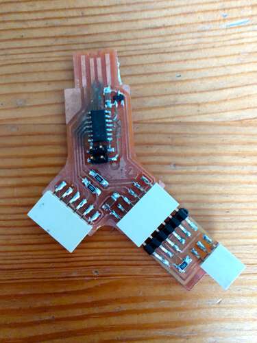
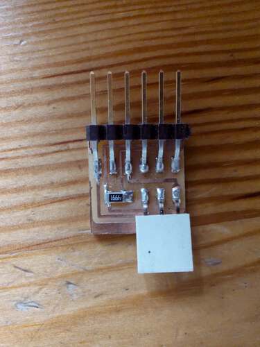
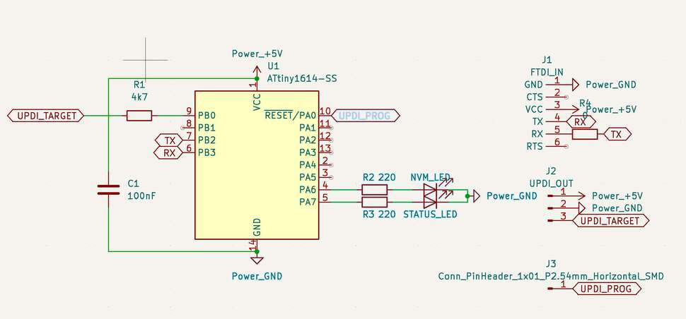
Sometimes, Serial UPDI proved to be a bit unstable so I found a way to program Attiny chips using JTAG2UPDI. This can be used to use any Arduip board as a UPDI programmer. I made a special board for this using an Attiny416, that acts as a JTAG2UPDI board but uses the same connectors as a SerialUPDI adapter.
 |
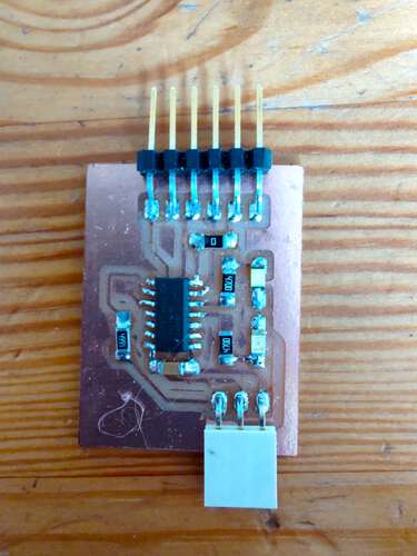 |
|---|---|
| The schematic for the jtag2updi board. | The final jtag2updi board. |
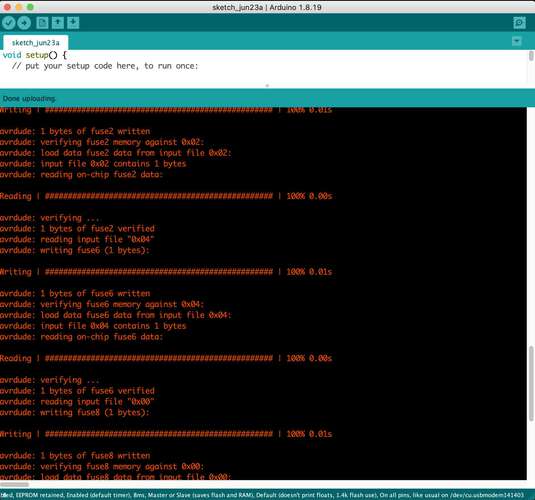
Programming the device using the arduino environment worked.
 |
 |
|---|---|
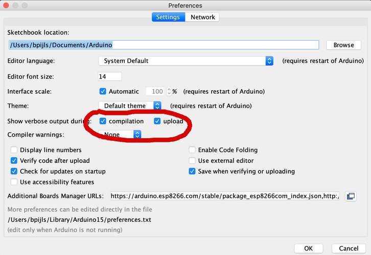
Setting the verbose flags in the Arduino preferences… |
…will result in more information being displayed in the Arduino console about the compiling and upload process |
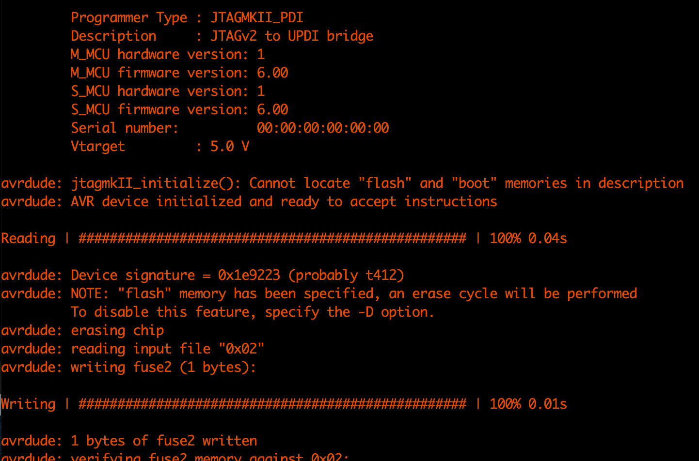 |
|---|
| The programmer is detected in the Arduino environment as a JTAG2UPDI programmer. |
My goals for this week were:
We didn’t play around too much with all the variables because it would probably end in tool-breakage. We did do a test milling the line-test and experience the difference between 1-flute and 2-flute milling bits.
I learned a lot from watching and experiencing the PCB milling process at de Waag. I adopted a lot of the strategies in my home lab. Specific learnings are described in the Make–>Learnings from Waag and FabAcademy section.
I have managed to mill a couple of boards at de Waag and I know enough about the workflow to mill more boards in the future.
Due to part failures and time constraints I have not been able to make a working programmer. I am quite positive I will manage to make one eventually.
I am extremely pleased with the success I had with my own 3018 PCB mill. I put a lot of time into tuning and upgrading the machine but I now know it is capable of milling PCBs with similar quality of the MDX-20 at de Waag. Obviously, the Chinese milling machine is far less reliable compared to a professional PCB milling machine, but I think I am going to have great use of this facility during the coming weeks at FabAcademy. I consider this to be time well spent.
Final project Initial conception (Febuary 2022) Learning to play any musical instrument takes a very long time and a lot of effort. To enjoy music …
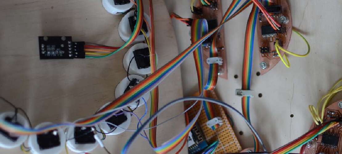
What I did. I created the enclosure and designed and milled all the PCBs. TODO Hardware Priority 1 20 x Button LED caps 8x Octave1 8x Octave2 4x chord …