Embedded Programming
Group Assignment 2021
WHAT IS A MICROCONTROLLER?
A microcontroller is a complete computer (microprocessor + I / O + memory + other peripherals), although of limited performance, which is contained in the chip of a programmable integrated circuit and is intended to govern a single task with the program that resides in its memory. Its input / output lines support the connection of the sensors and actuators of the device to be controlled.
DIFFERENCE BETWEEN MICROPROCESSOR AND MICROCONTROLLER
The microprocessor is an integrated circuit that contains the Central Processing Unit (CPU), also called a processor, of a computer. The CPU is made up of the Control Unit, which interprets the instructions, and the data path, which executes them.
The pins of a microprocessor bring out the lines of its address, data and control buses, to allow it to connect with the Memory and I/O Modules and configure a computer implemented by various integrated circuits. A microprocessor is said to be an open system because its configuration varies according to the application for which it is intended.
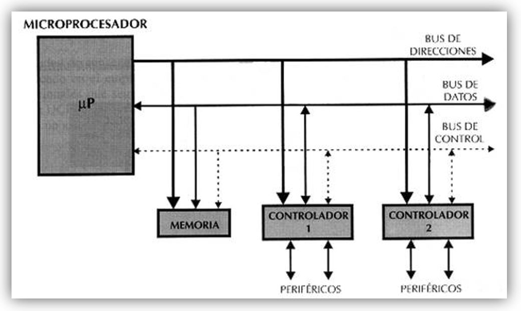
Structure of an open system based on a microprocessor. The availability of buses abroad allows it to be tailored to the application.
If only one microcontroller model was available, it should have all its resources highly enhanced to be able to adapt to the demands of different applications. In practice, each microcontroller manufacturer offers a large number of different models, from the simplest to the most powerful. It is possible to select the memory capacity, the number of I / O lines, the quantity and power of the auxiliary elements, the operating speed, etc. Therefore, a very prominent aspect of the design is the selection of the microcontroller to use.
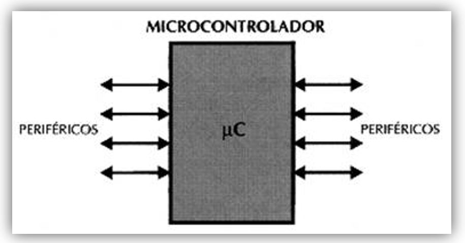
The microcontroller is a closed system. All the parts of the computer are contained in its interior and only the lines that govern the peripherals go out to the outside.
TYPES OF ARCHITECTURES:
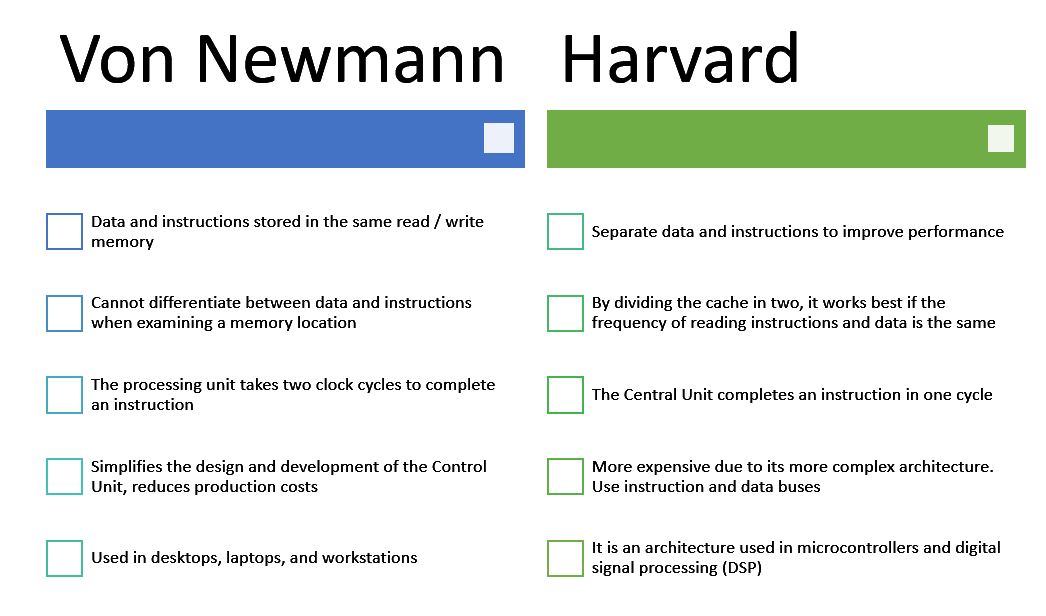
VON NEUMANN ARCHITECTURE:
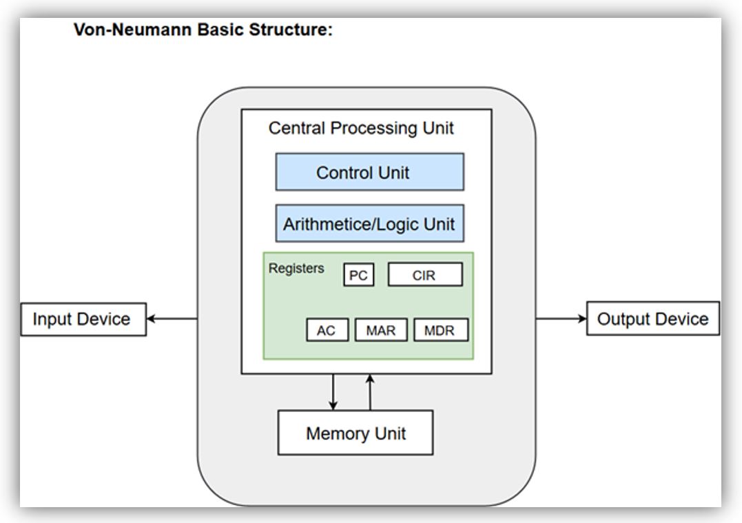
Most of the current computer systems follow the architecture proposed by Von Newmann.
Von Newmann created a model that is characterized by having a single main memory in which the instructions are stored.
Von Newmann's architecture is made up of the CPU (Central Processing Unit) which, in turn, contains:
* An ALU (Arithmetic Logic Unit)
* Processor registers
* A control unit
* A program counter
The ALU is in charge of carrying out arithmetic operations (addition, subtraction, multiplication, division, ...) and logic (AND, OR and NOT).
The processor registers are a small memory that stores binary data and has an access time five to ten times less than the main memory, one of the registers is called PROGRAM COUNTER and it is the one that automatically calculates the number of execution cycles.
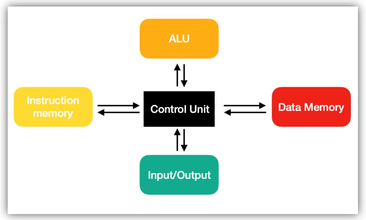
The Control Unit is in charge of reading the instructions of the programs stored in memory and sending the orders to the processor components to execute the instructions.
Main memory is a set of cells of the same size that are associated with a number called a memory address and serve to temporarily store data for later use.
This main memory, in computer systems, is usually made up of two different areas:
** RAM Memory (Random Access Memory): is that destined to the storage of data and programs including the Operating System.
** ROM (Read Only Memory): used for storing small programs for basic resource management, especially input and output.
HARVARD ARCHITECTURE:
This type of architecture was created by Howard H. Aiken. It is an architecture where instructions and data are stored in separate caches to improve performance.
The Harvard architecture is simpler than the Von Newmann, this reason makes it much faster, for electronic circuits (such as those used in refrigerators, washing machines, audio devices, video devices, ...). It takes fewer steps to process.
The Harvard architecture can execute the data and execute the operations at the same time because each of these has its own address bus.
Modern uses of Harvard architecture:
*** Digital signal processors (DSPs) run small highly optimized audio or video processing algorithms. They avoid caches because their behavior must be extremely reproducible. The difficulties of dealing with multiple address spaces are a secondary concern to execution speed. Consequently, some DSPs have multiple data stores in different address spaces to facilitate both SIMD and VLIW processing. As an example, Texas Instruments TMS320 C55x processors have several parallel data buses (two write, three read) and an instruction bus.
*** Microcontrollers are characterized by having small amounts of program (flash memory) and data memory (SRAM), without cache, and take advantage of the Harvard architecture to accelerate processing through simultaneous access to instructions and data. Separate storage means that memories can differ in bit widths, for example using 16-bit wide instructions and 8-bit wide data. This also means that instructions can be brought in before they are needed (prefetching) while other activities take place in parallel. Examples include AVR from Atmel Corp and PIC from Microchip Technology, Inc ..
COMPARISON BETWEEN VON NEWMANN AND HARVARD
CISC AND RISC ARCHITECTURE:
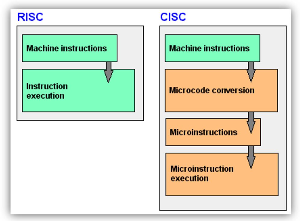
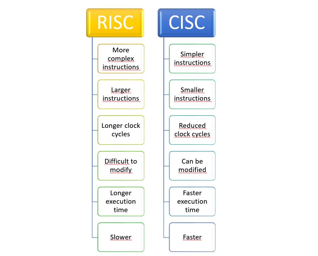
In the CISC (Complete Instruction Set Computer) architecture the instruction set is much larger and more complex than in the RISC (Reduced Instruction Set Computer) architecture. The clock cycles are longer and longer, this is due to the amount of instructions.
The CISC architecture relies on micro-code to cope with the most complex operations and minimizes instructions to increase clock cycles and their time. Although, sometimes clock cycles must be slowed down to give enough time to complete instructions.
For this reason, with the CISC architecture it is advisable to shorten the code since the cycles require time to be executed. It is an architecture that is more difficult to modify due to its complexity.
Instead, its use favors software costs and instruction set compatibility.
Examples of them are: Motorola 68000, Zilog Z80 and the entire Intel x86 family used in most of today's personal computers.
In the RISC architecture (Reduced Instruction Ser Computer) the set of instructions is smaller and reduced, in its construction, it has fewer transistors, which makes it cheaper to manufacture and is capable of minimizing clock cycles.
The control is done by wiring to make it easier to channel the instructions, but it is more difficult to deal with at the hardware level.
If a new instruction needs to be added, it must be taken into account that it is not large or stall the execution cycle. On the other hand, if this does not happen, keep in mind that it can process 2 to 4 times faster than the CISC architecture.
Examples: PowerPC, DEC Alpha, MIPS, ARM, SPARC ... are examples of some of them.
COMPARISON BETWEEN CISC AND RISC
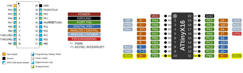
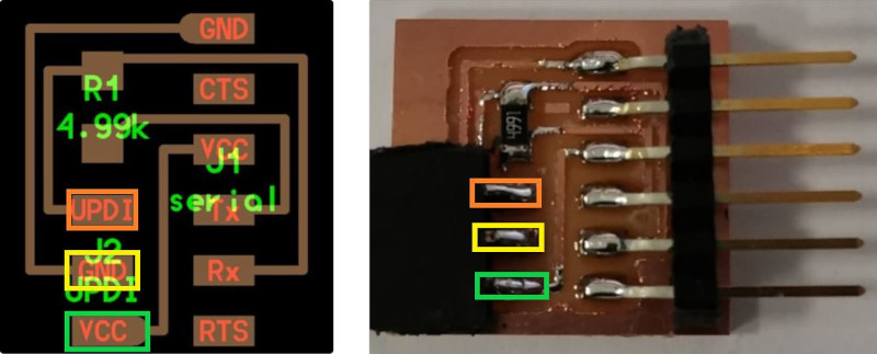
ATtiny3216 Microcontroller
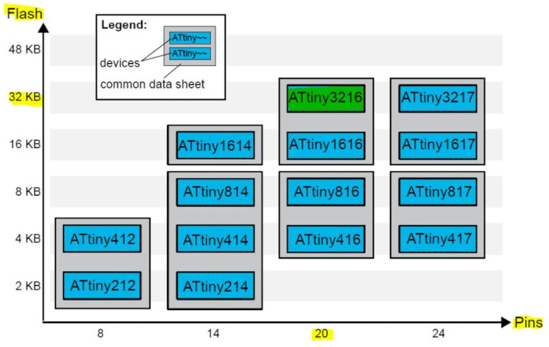
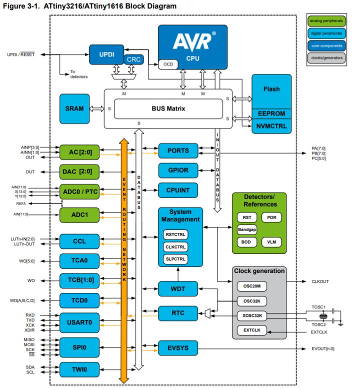
I find information about the ATtiny3216 on the SpenceKonde website.
In the CISC (Complete Instruction Set Computer) architecture the instruction set is much larger and more complex than in the RISC (Reduced Instruction Set Computer) architecture. The clock cycles are longer and longer, this is due to the amount of instructions.
* Pack of 20 pins.
* Internal clocks 1/4/5/8/10/16 20 MHz.
* 32768 bytes flash memory.
* 256 bytes EEPROM and 2048 bytes SRAM.
* Maximum voltage: 6V; minimum voltage -0.5 V.
* VDD: Supply voltage. GND: ground.
* Digital pins: Port A: PA0, PA1, PA2, PA3, PA4, PA5, PA6, PA7. Port B: PB0, PB1, PB2, PB3, PB4, PB5. Port C: PC0, PC1, PC2, PC3.
* Analog pins: Port A: PA0, PA1, PA2, PA3, PA4, PA5, PA6, PA7. Port B: PB0, PB1, PB4, PB5.
* UPDI programming pin: PA0 (physical pin number 16).
Within the communications section there are different types and their pins are different. It is clear that the different communication protocols cannot all be used at the same time, because they have pins in common.
* USART - Universal and Asynchronous Synchronous Receiver and Transmitter: It has the RX (PB3 or PA2) and the TX (PB2 or PA1).
* SPI - Serial Peripheral Interface: It only has MOSI (PA1 or PC2), MISO (PA2 or PC1), SCK (PA3 or PC0), SS (PA4 or PC3).
* TWI - Two Wire Interface (I2C): Has SDA (PB1 or PA1) and SCL (PB0 or PA2).
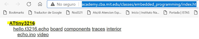
I find information about a Neil board "hello.t3216" in the week of embedded programming.
I am guided by this board for the design, but I'm going to create my board by enabling all the connection pins of the ATtiny3216.
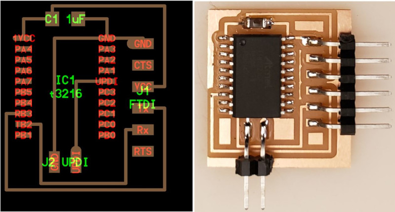
In addition, I will be guided by what Adrian Torres did using an " ATtiny3216 board" in the week of in Input Device.
Workflow with the ATtiny3216 microcontroller
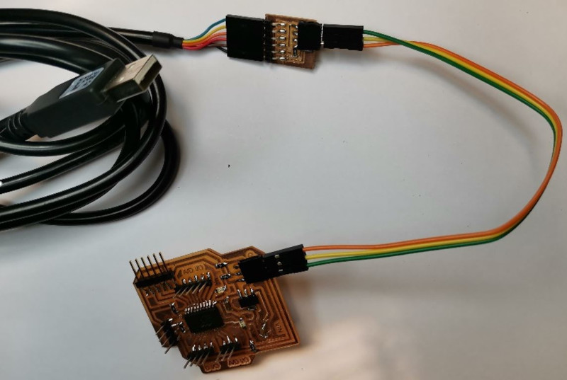
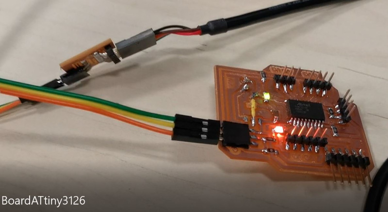
To program the ATtiny3216 I use the FTDI / UPDI connector that I manufactured in week 4 Electronic Production.
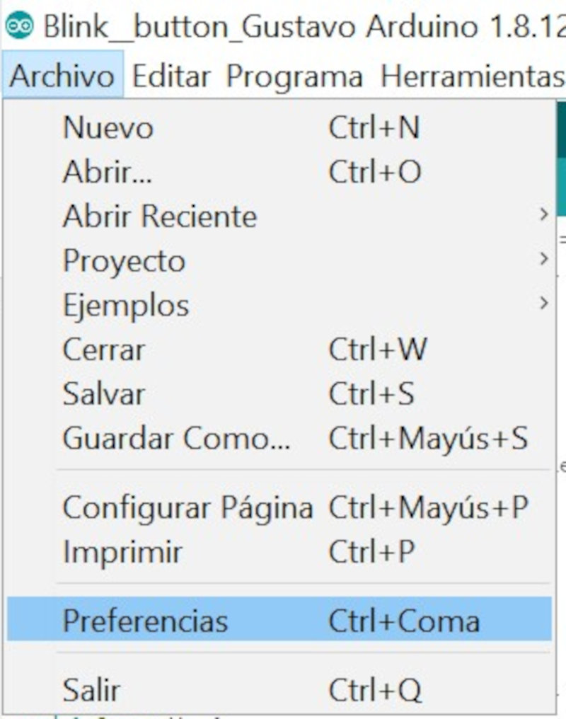
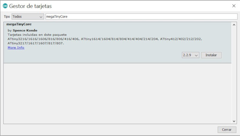
I have followed the following tutorial SpenceKonde/megaTinyCore for the installation of Boards Manager in Arduino. Open Arduino IDE.
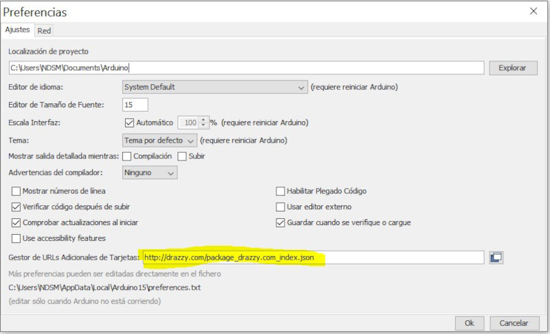
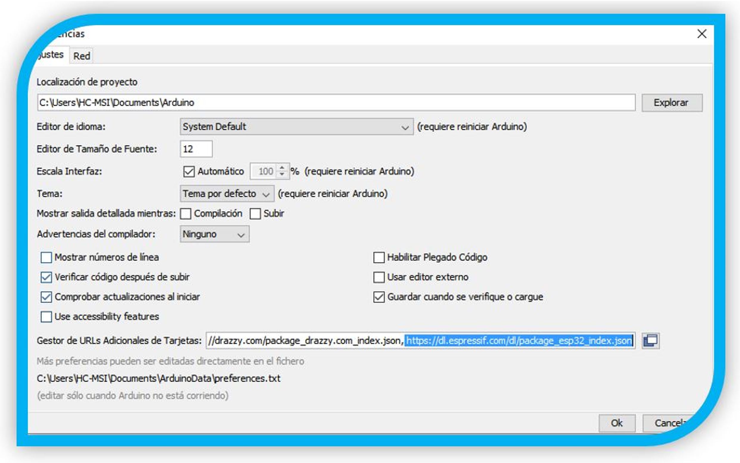
1. File -> Preferences, please enter the above url in "Additional urls of dashboard manager". The boards manager URL is: http://drazzy.com/package_drazzy.com_index.json
2. Tools -> Dashboards -> Dashboard Manager ...
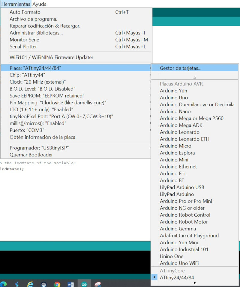
3. Select "Spence Konde megaTinyCore" and click "Install". For best results, choose the latest version.
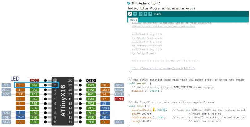
I use Arduino IDE and first load an example program "blink" and select the pinout = 0 that I use for the LED of my board, so I check that the board works correctly.
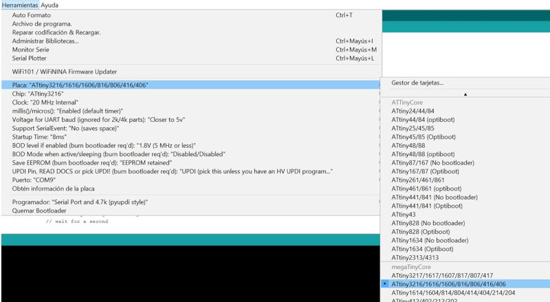
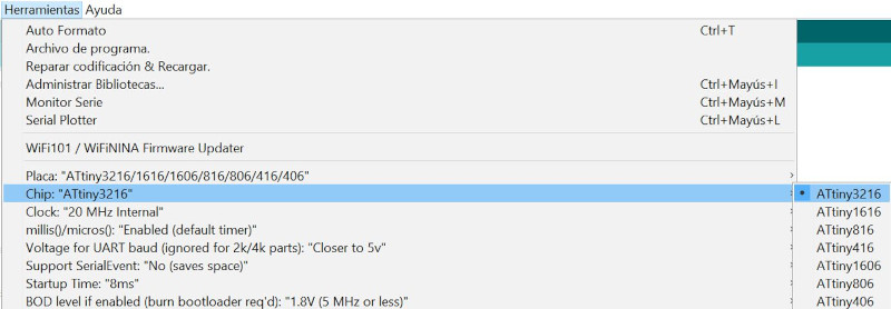
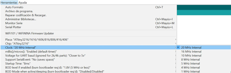
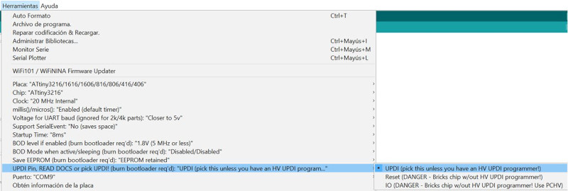
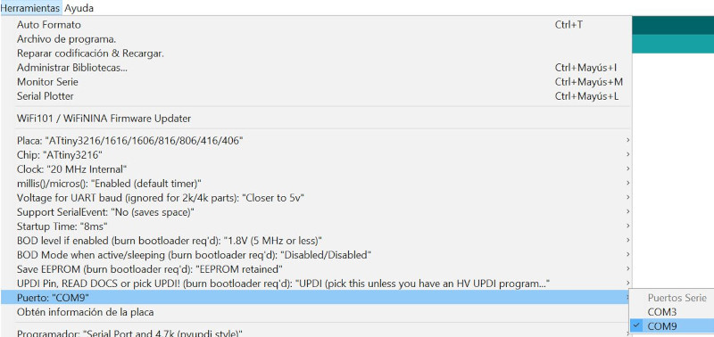
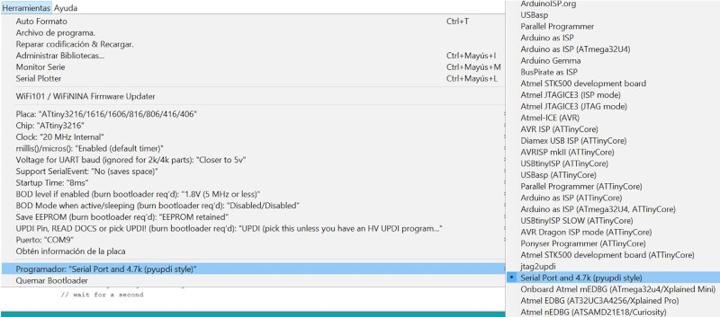
In Tools I modify the parameters to program the ATtiny3216.
I configure the Arduino IDE for the ATtiny 3216; I set the clock to 20MHz and in my case the communication port with the COM3 microcontroller. It is important to have the FTDI-USB connected and choose the "Serial Port and 4.7k programmer (pyupdi style)".
ESP32 Microcontroller
Processors:
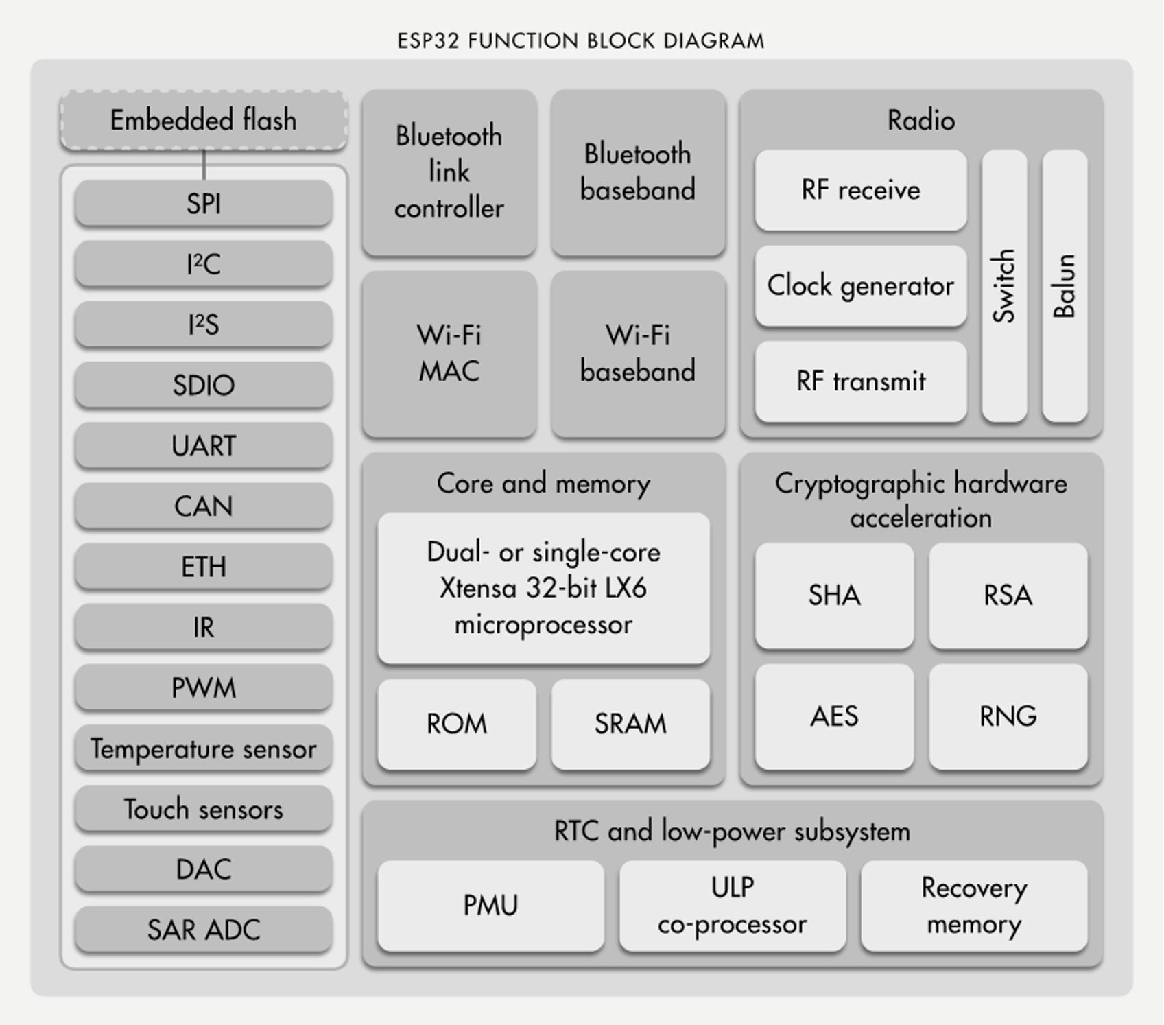
* Main processor: Tensilica Xtensa 32-bit LX6 microprocessor
* Cores: 2 or 1 (depending on variation)
All chips in the ESP32 series are dual-core except for ESP32-S0WD, which is single-core.
* Clock frequency: up to 240 MHz
* Performance: up to 600 DMIPS
* Ultra low power co-processor: allows you to do ADC conversions, computation, and level thresholds while in deep sleep.
Wireless connectivity:
* Wi-Fi: 802.11 b/g/n/e/i (802.11n @ 2.4 GHz up to 150 Mbit/s)
* Bluetooth: v4.2 BR/EDR and Bluetooth Low Energy (BLE)
Memory:
* Internal memory: ROM 448 KiB
For booting and core functions
* SRAM: 520 KiB
For data and instruction.
* RTC fast SRAM: 8 KiB
For data storage and main CPU during RTC Boot from the deep-sleep mode.
* RTC slow SRAM: 8 KiB
For co-processor accessing during deep-sleep mode.
* eFuse: 1 Kibit
Of which 256 bits are used for the system (MAC address and chip configuration) and the remaining 768 bits are reserved for customer applications, including Flash-Encryption and Chip-ID.
* Embedded flash:
Flash connected internally via IO16, IO17, SD_CMD, SD_CLK, SD_DATA_0 and SD_DATA_1 on ESP32-D2WD and ESP32-PICO-D4.
* 0 MiB (ESP32-D0WDQ6, ESP32-D0WD, and ESP32-S0WD chips)
* 2 MiB (ESP32-D2WD chip)
* 4 MiB (ESP32-PICO-D4 SiP module)
External flash & SRAM: ESP32 supports up to four 16 MiB external QSPI flashes and SRAMs with hardware encryption based on AES to protect developers' programs and data. ESP32 can access the external QSPI flash and SRAM through high-speed caches.
* Up to 16 MiB of external flash are memory-mapped onto the CPU code space, supporting 8-bit, 16-bit and 32-bit access. Code execution is supported.
* Up to 8 MiB of external flash/SRAM memory are mapped onto the CPU data space, supporting 8-bit, 16-bit and 32-bit access. Data-read is supported on the flash and SRAM. Data-write is supported on the SRAM.
ESP32 chips with embedded flash do not support the address mapping between external flash and peripherals.
Peripheral input/output: Rich peripheral interface with DMA that includes capacitive touch, ADCs (analog-to-digital converter), DACs (digital-to-analog converter), I²C (Inter-Integrated Circuit), UART (universal asynchronous receiver/transmitter), CAN 2.0 (Controller Area Network), SPI (Serial Peripheral Interface), I²S (Integrated Inter-IC Sound), RMII (Reduced Media-Independent Interface), PWM (pulse width modulation), and more.
• Security:
* IEEE 802.11 standard security features all supported, including WFA, WPA/WPA2 and WAPI
* Secure boot
* Flash encryption
* 1024-bit OTP, up to 768-bit for customers
* Cryptographic hardware acceleration: AES, SHA-2, RSA, elliptic curve cryptography (ECC), random number generator (RNG)
Workflow with the ESP32 microcontroller
1. Choose a programming environment, for example, Arduino ID.
2. Download the necessary libraries for the microcontroller in this case:
and an example video.
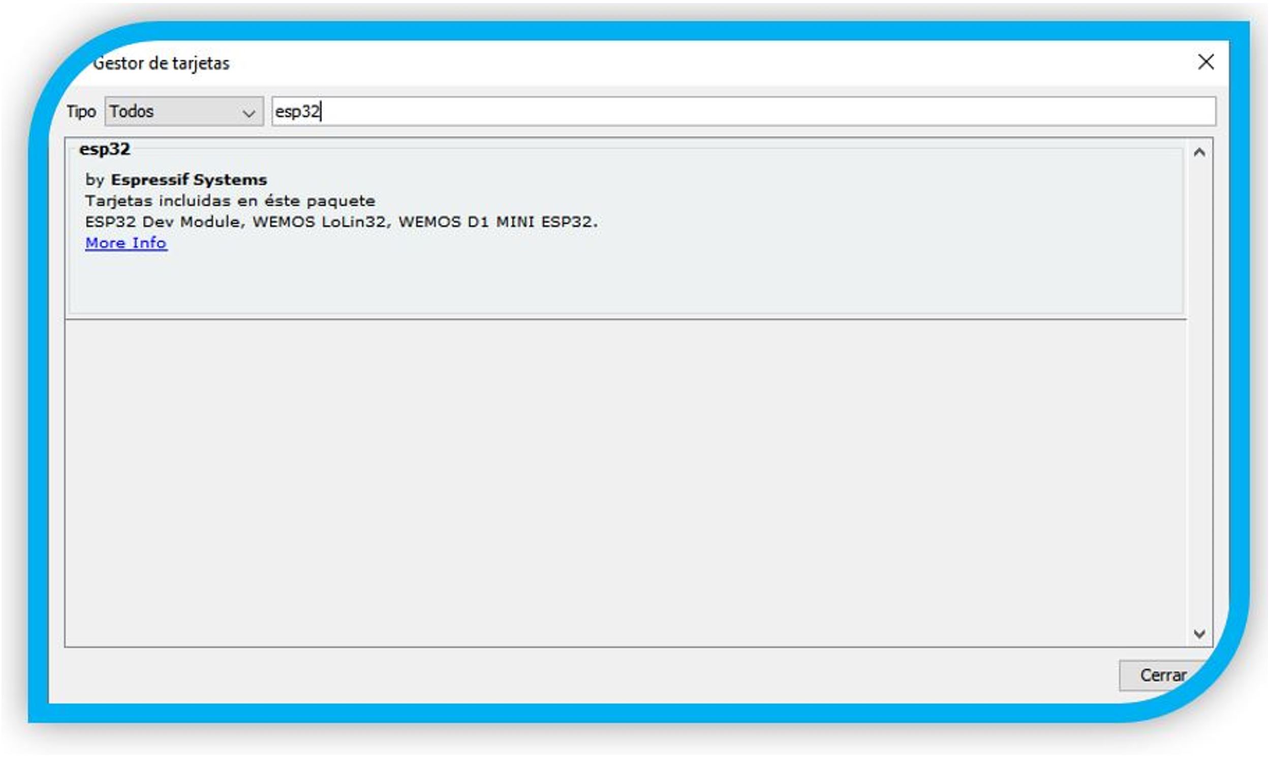
3. Install the board in the Board Manager:
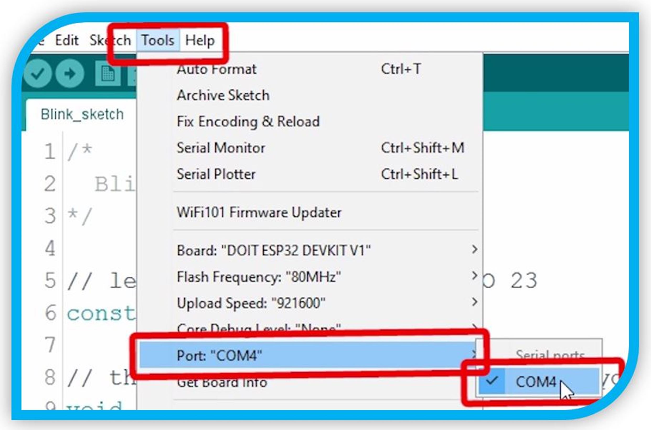
4. Select the board and the port to which it is connected (to connect the electronic board, in this case the FTDI cable has been used):
5. From here, it is to create the program code in Arduino ID, or to upload an example or a created code.
6. Burn the code. At this point, with the ESP32 it is necessary to put the switch in the programming position and also press the reset button.
7. When the electronic board is already programmed, the switch is put into operation mode, and it is ready to operate.