Electronics design
EDA
This week promising to be interesting because it’s totally new field for me. I’ve chosen KiCad for electronics design because I want to learn more open-source tools which are providing great flexibility and community support. Of course open-source sometimes not so polished and straightforward as commercial counterparts but, I think, through exploring new software, finding new work-flows, bugs and workarounds — learning happens.
KiCad
KiCad is an open source tool with great amount of support. There are a lot of component libraries with footprints and 3D models. The software itself is more like a bunch of separate programs. Not very easy for starters but once you get in it’s not hard to put it all together.
Eschema
Designing electronics usually begins from schematics. This drawing represents all components relations but not the spatial layout. In KiCad this task accomplished in Eschema module.
After downloading FabLab libraries and installing them, open KiCad and then Eschema
▼ Use Place Symbol ▶ press anywhere on a sheet ▼ Find a component and confirm ▼ Place a component on the sheet ◔ Repeat for each component
▼ Connect pins using Place Wire
Here I’m using wire connections but also it can be done using labels and both.
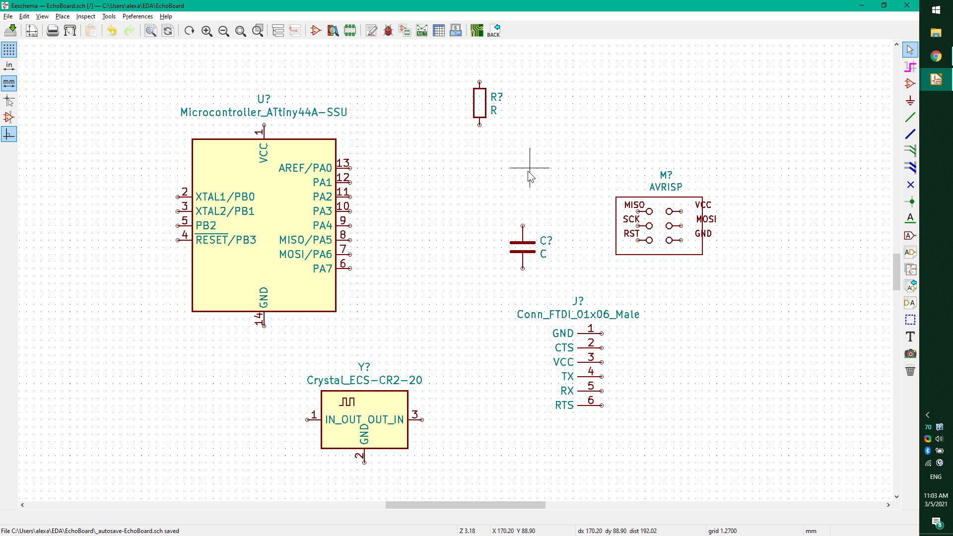
▼ Recheck the layout
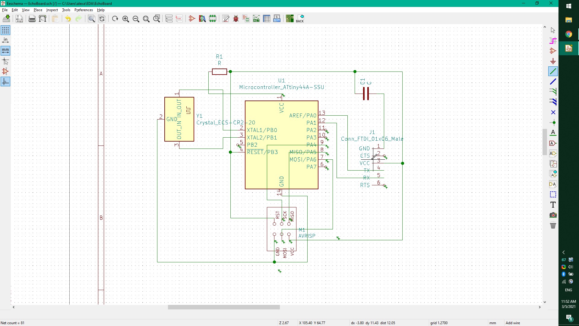
◉ The scheme is ready now
▼ Press Generate netlist on the top bar ▼ Press Generate netlist in popup window and save the file ⬤ Netlist is ready for Pcbnew
Pcbnew
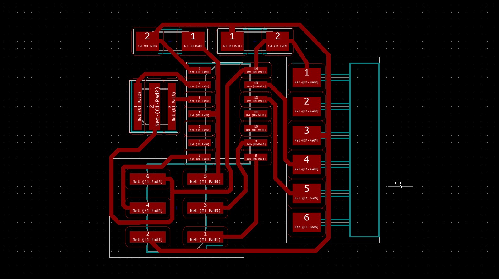
The next piece in KiCad’s puzzle is Pcbnew. This program is for traces routing. It’s taking the generated net list and importing components footprints (where the component’s pins are) with relations displayed in graphical lines. Then it assists while routing (drawing) highlighting the correct destination pad.
▼ Open Pcbnew ▶ press Load Netlist on the top panel ▼ choose netlist file in pop up window ▼ press Update PCB and Close ▼ position footprints inside the sheet
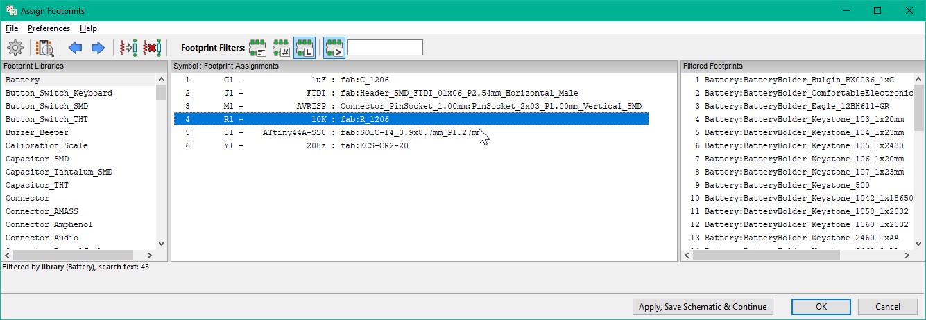
KiCad imports footprints according to the library used in Eschema. I’m using only SMD components for this board but KiCad imported one footprint for through hole soldering. The correct footprint must be assigned through Eschema and updated into the net list.
▼ Open Eschema ▶ press Assign PCB footprint to schematic symbols ▼ choose the symbol in the middle section ▼ look for correct footprint in the right section ▼ double-click the footprint to assign it to the symbol ▼ press OK
It is possible to assign names to each pad for better orientation while routing
▼ Double-click on the pad
▼ type pin name into Pad number: field
⬤ The traces are ready for exporting
KiCad allows exporting in different formats. In my work-flow I’m exporting into SVG and then using InkScape to create outline file. In order to export the traces in Pcbnew.
▼ Press File ▶ Export ▶ SVG...
▼ choose Output directory
▼ select the layers to export
▼ press Export
⬤ now the file is saved in the project folder
InkScape
I’m using InkScape to process the SVG and output two files. The outline file is the rectangle that offsetting file boundaries by 0.8 mm which is the diameter of cutout bit. The traces file must have the same sheet size as the outline file has, but actual cutout path could be any shape until it is not interfering with the wiring.
▼ Process the SVG into two similarly dimensioned files
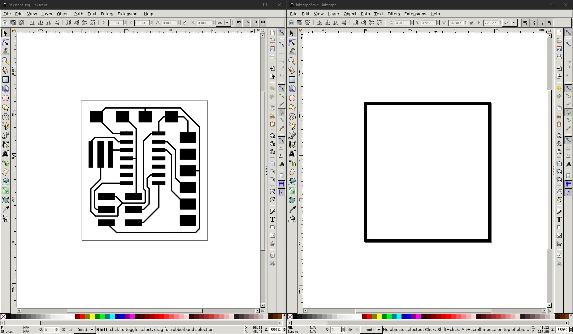
▼ Check the traces for any drawing errors
MODS
To produce .rml file I’m using MODS. I already played with it on the Week 04 with .png input. Now I will use .svg to produce the path.
▼ Select the server program
▼ Invert the svg and use the same steps as in traces path
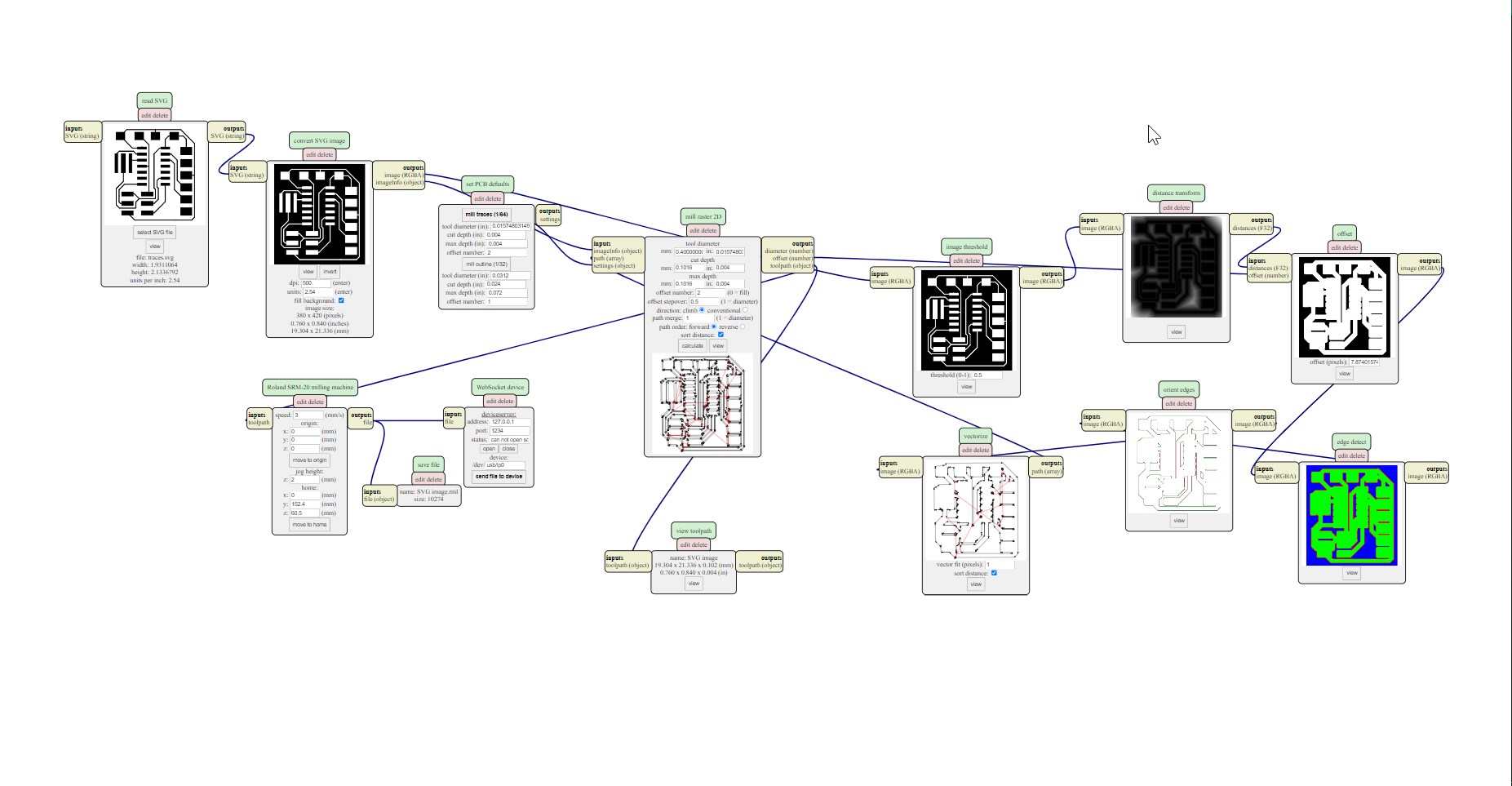
▼ Generate traces outline
Something went wrong and the outline SVG didn’t produce path correctly, but inverted SVG did.
▼
Milling
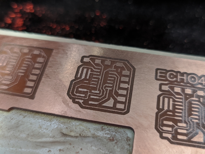
Aimed for creating really tiny traces I have milled several boards. The traces width was 0.2 mm, and to succeed it took 4 attempts.
▼ The first try
In the first try there was several problem spots. In one spot traces was touching and in other they were just milled away.
▼ The second try
Here, I have adjusted traces file in the problem spots increasing the distance between the traces ensuring there is enough space for bit to mile between preserving configuration.
The one thing I’ve tried in this attempt is changing the climb direction to conventional. The traces were completely destroyed. For some reason this setting just destroyed every trace on the board
.
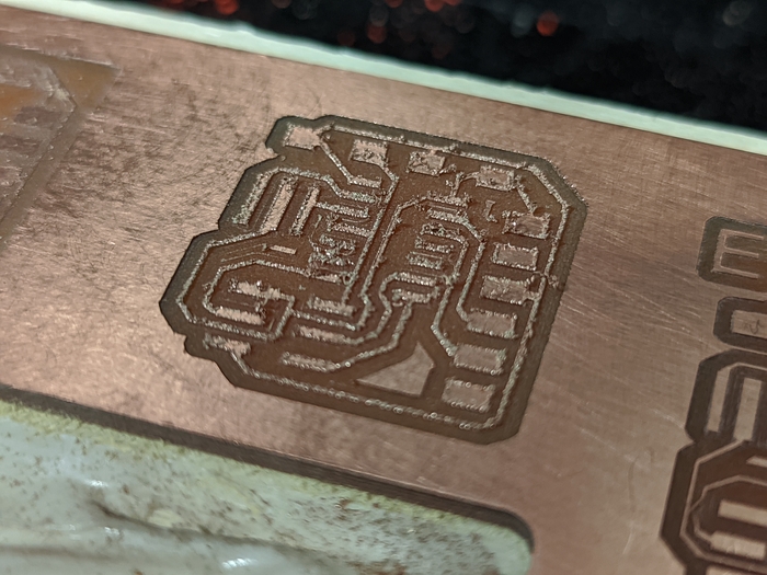
▼ The third attempt
This time I’ve changed the direction back to
climband traces went back, but the only one weak spot remained. Very tiny trace just cracked as soon as I’ve touched it.
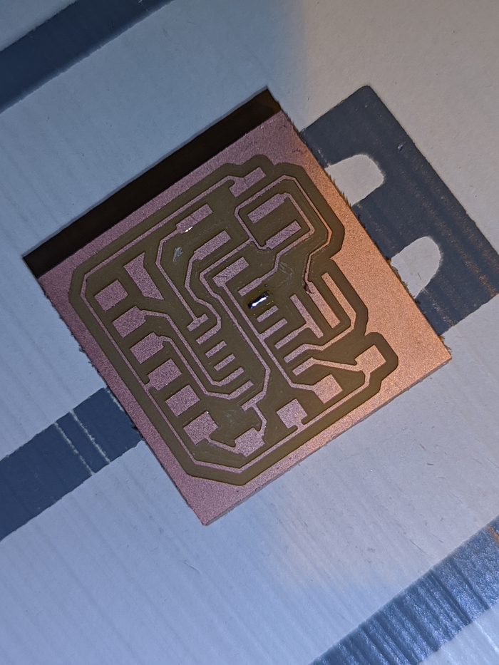
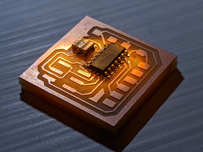
Here after 3 attempts 0.2 mm traces finally preserved. I was happy about the results, but…
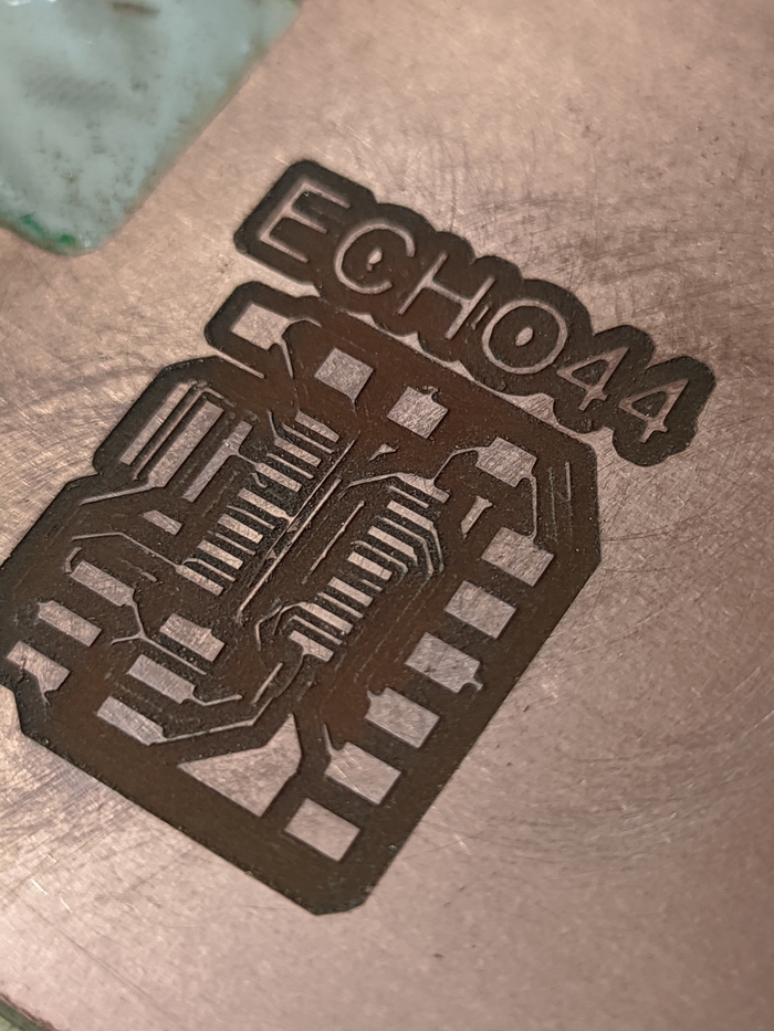
▼ Attempt #4
▼ The cutout
I missed the size of the ISP connector’s footprint. That meant that I need to adjust the traces file, and as I was running out of time I decided to adjust all the traces for 0.35 mm width to be sure it will succeed from the firs try.
▼ The missed footprint size
▼ The final layout with 0.35 mm traces
Lockdown kit
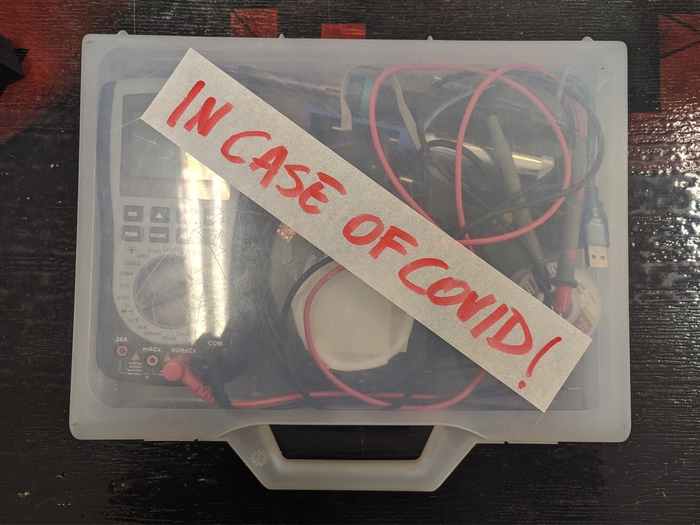
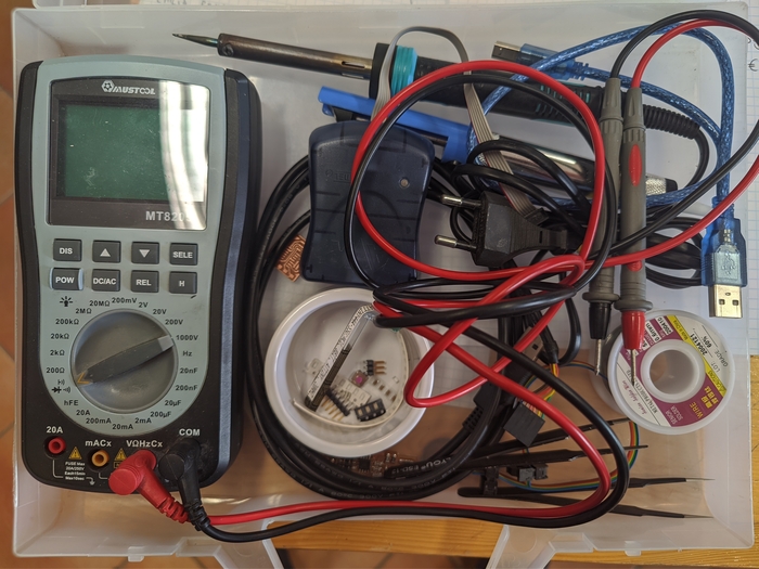
Unfortunately this week COVID restriction measures had to begin on Monday. My instructor supplied me with all the needs to work at home.
▼ COVID case
Soldering
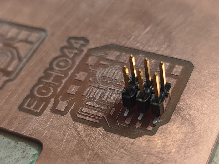
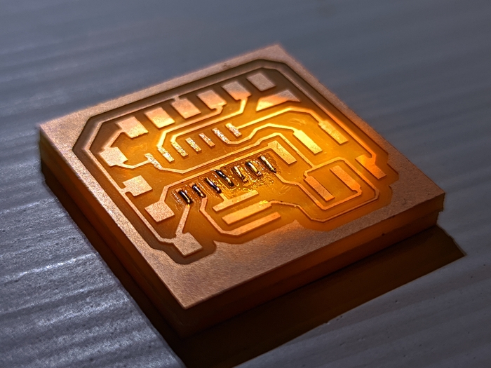
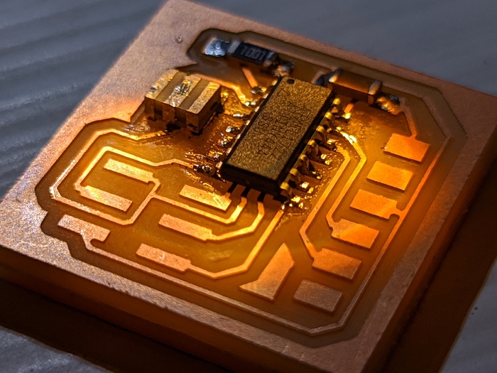
Armed wit an iron all some equipment from the lab, I’ve continued my journey at home. The final piece came out really nice. The 0.34 traces are robust and clean.
▼ The final attempt #5
MCU
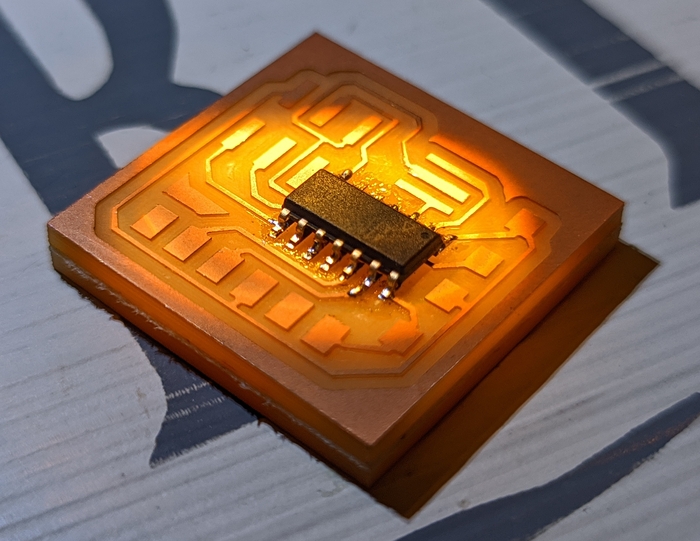
Using same steps described in Week 04 soldering section I’ve begun the process.
▼ First pad covered with tin
▼ Attiny side row covered with tin
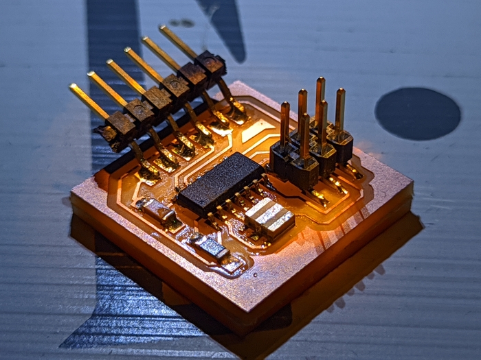
▼ MCU mounted
Crystal
▼ 20hz crystal is mounted
More
▼ Resistor and capacitor are mounted
All mounted
▼ Fully soldered board
Check
Using multimeter I’ve checked the board for shorts and checked the connections.
▼ Check the traces
Programming
Usbtiny
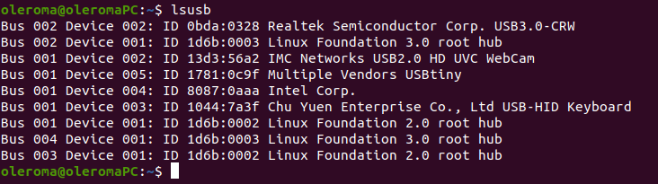
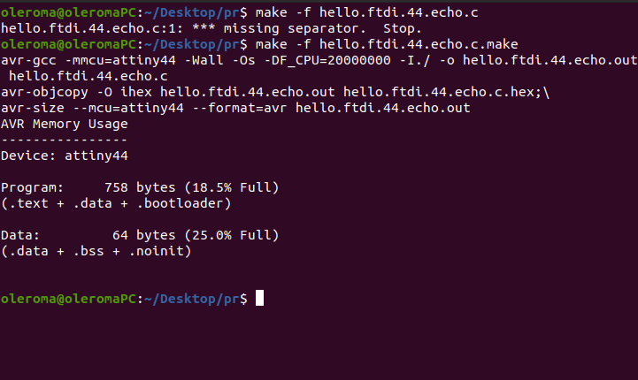
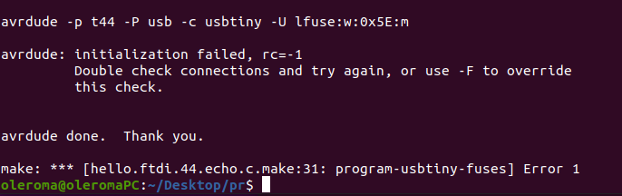
Now I’m running my Ubuntu to program the board. I’ve tried to use my Usbtiny programmer, but something was wrong. Initialization was failing and I switched to AVRisp programmer.
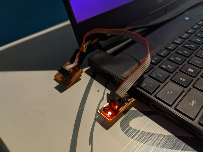
▼ Using Usbtiny programmer
▼ Make sucseeded
▼ Initialization failed
Avrisp2
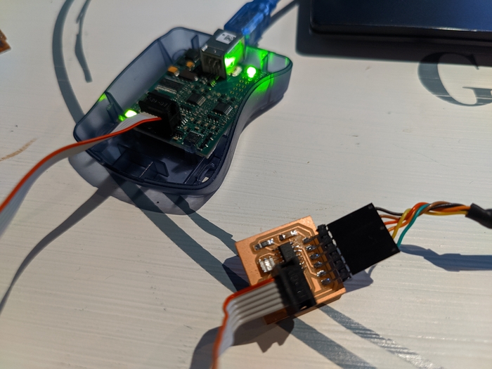
From this point, I’m using Avrisp2 to flash the board. No success, maybe something is wrong with the board components or soldering.
▼ Using avrisp2
The issue
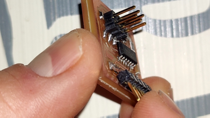
Looking into the board searching for issues I’ve discovered that one of the ATtiny’s legs was slightly off the pad’s surface. I didn’t notice this and hope this will fix the issue now.
▼ Bad soldering
Microchip studio
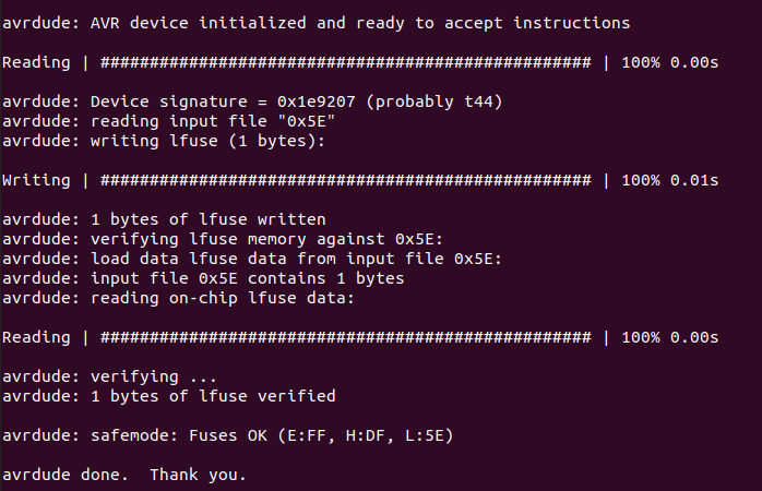
Fixing the leg didn’t fix the programming. Now the process fails after programming the fuses. As I’ve been following the FabAcademy tutorial on “Embedded programming”, I was not able to succeed because of missing paragraph related to setting the low fuse to 0x5E. Trying to resolve the issue at home I looked into the C code from lecture page and noticed the line saying “set lfuse to 0x5E for 20 MHz xtal”. Googling for this for some reason was not effective and I recalled that I have installed the microchip studio from Atmel on Windows. I’ve switched to windows and through Microchip studio’s device programming tool was able to set the low fuse to needed value. After that, programming worked in Linux.
▼ Setting low fuse in Microchip studio
▼ Fuses programmed
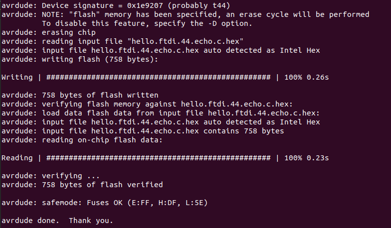
▼ The code is flashed onto the attiny
Checking the results with MODS
To check the results I’ve used locally installed MODS just following the steps described in Embedded programming lecture page. This worked and now my Attiny is typing back characters I’m typing in. For that I’ve used server that goes with MODS installation.
▼ Communicating through serial in mods
OK, it works! Now I need to dive into Embedded programming to understand what steps under Ubuntu was missed. The further steps would require me to establish operational toolchian under one OS to be able flashing my devices with ease.